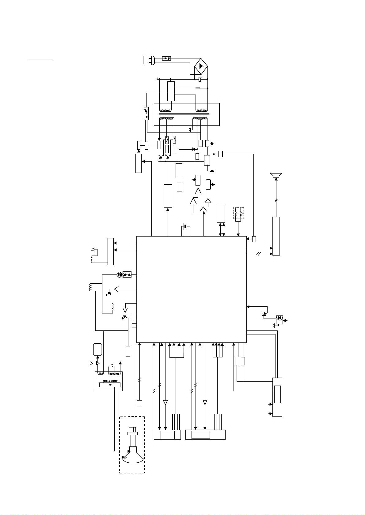
Sanyo CE25DN9-B User manual

Part No. SKSM0711 C5VRL JUNE 2004
Colour Television
Service Manual
Model CE25DN9-B
Service Ref. No. CE25DN9-B-01
PRODUCT CODE: 111360913
ORIGINAL VERSION: Chassis No. EB8-A
Give complete "SERVICE REF. NO." for parts
order or servicing, it is shown on the rating sheet
on the cabinet back of the TV set.
Note
This TV receiver will not work properly in foreign
countries where the television transmission
system and power source differ from the design
specifications. Refer to the specifications for the
design specifications
CE25DN9-B
Contents
Safety precautions/Specifications ..................................................................................................................2
Block diagrams ..............................................................................................................................................3
Cabinet Disassembly......................................................................................................................................4
Adjustment and Repair Procedures............................................................................................................5~9
CPU Functions ..............................................................................................................................................................................10~11
Component Locations ..................................................................................................................................12
IC Block Diagrams..................................................................................................................................13~15
Pin description of semiconductors................................................................................................................16
Part Description and reading of schematic diagram ....................................................................................17
Cabinet Parts List/TV Stand parts list ..........................................................................................................18
Electric Parts List....................................................................................................................................19~24
Please use Schematic Diagram SKP20435
inserted with this Service Manual.

Part No. SKSM0720 C7WAS JULY 2004
Colour Television
Service Manual
Model CE28DN9-B
Service Ref. No. CE28DN9-B-01
PRODUCT CODE: 111373100
ORIGINAL VERSION: Chassis No. EB8-A
Give complete "SERVICE REF. NO." for parts
order or servicing, it is shown on the rating sheet
on the cabinet back of the TV set.
Note
This TV receiver will not work properly in foreign
countries where the television transmission
system and power source differ from the design
specifications. Refer to the specifications for the
design specifications
CE28DN9-B
Contents
Safety precautions/Specifications ..................................................................................................................2
Block diagrams ..............................................................................................................................................3
Cabinet Disassembly......................................................................................................................................4
Adjustment and Repair Procedures............................................................................................................5~9
CPU Functions ..............................................................................................................................................................................10~11
Component Locations ..................................................................................................................................12
IC Block Diagrams..................................................................................................................................13~15
Pin description of semiconductors................................................................................................................16
Part Description and reading of schematic diagram ....................................................................................17
Cabinet Parts List ........................................................................................................................................18
Electric Parts List....................................................................................................................................19~24
Please use Schematic Diagram SKP20443
inserted with this Service Manual.

-2-
C7WAS
SAFETY PRECAUTION
X-RADIATION PRECAUTION
The primary source of X-RADIATION in the television receiver is the picture tube. The picture tube is specially
constructed to limit X-RADIATION emissions. For continued X-RADIATION protection, the replacement tube
must be the same type as the original including suffix letter. Excessive high voltage may produce potentially
hazardous X-RADIATION. To avoid such hazards, the high voltage must be maintained within specified limit.
Refer to this service manual, high voltage adjustment for specific high voltage limit. If high voltage exceeds
specified limits, take necessary corrective action. Carefully follow the instructions for +B1 volt power supply
adjustment, and high voltage adjustment to maintain the high voltage within the specified limits.
PRODUCT SAFETY NOTICE
SPECIFICATIONS
Product safety should be considered when a component replacement is made in any area of a receiver.
Components indicated by mark in the parts list and the schematic diagram designate components in which
safety can be of special significance. It is particularly recommended that only parts designated on the parts list in
this manual be used for component replacement designated by mark . No deviations from resistance wattage
or voltage ratings may be made for replacement items designated by mark .
!
!
!
1: An isolation transformer should be connected in the
power line between the receiver and the AC line
when a service is performed on the primary of the
converter transformer of the set.
2: Comply with all caution and safety-related notes
provided on the cabinet back, inside the cabinet, on
the chassis or the picture tube.
3: When replacing a chassis in the cabinet, always be
certain that all the protective devices are installed
properly, such as, control knobs, adjustment covers
or shields, barriers, isolation resistor-capacitor networks
etc. Before returning any television to the customer,
the service technician must be sure that it is completely
safe to operate without danger of electrical shock.
Power source AC 220~240V, 50Hz
Television system System I
Colour system PAL/NTSC4.43 (PAL/NTSC4.43/NTSC3.58 IN AV MODE)
Receiving channel UHF: #21~69
Aerial input impedance 75ohm
Rear AV terminal
AV1: CENELEC standard
INPUT: Composite video, RGB and Audio L/R
OUTPUT: TV-output with composite video and audio L/R
AV2: CENELEC standard
INPUT: Composite video, RGB, S-VHS and Audio L/R
OUTPUT: Monitor output with composite video and Audio L/R
Front AV terminal
AV3: RCA jacks
INPUT: Composite video and Audio L/R
Sound output(Music) 5 x 2
Dimensions (WxHxD) 736 x 597 x 494mm
Weight 30.7Kg

-3- C7WAS
BLOCK DIAGRAM
This is a diagram for all models and therefore differs slightly from the actual block diagram.
IC601
TN6Q04
C609
D610
14v IC645
5v
P.F
2
4
1
25v
D671
7v
3v3
ON/OFF
UOC PIN 107
Q651
Q642
+14v
-14v
Q625
Q682
145v
Q641
Q675 St-BY UOC
PIN 106
AC
A101
TUNER
X122
X121
5v30v
5
A1901
RC RECEIVER
PF
Q866
IC001
AUDIO AMPLIFIER
SPEAKER
SP901
SP902
KEY SW
IC801
MEMORY
1V8_1 Q202 Q201
1V8_2 Q203
Q204
TO UOC PINS
93 & 96
TO UOC PINS
3,100,117,118,124
UOC
Q1001
Q1002
SC_1 B-IN
SC_1 G-IN
SC_1 R-IN
SC1 FB IN
K1001
SCART 1
SC_1 VIDEO OUT
SCART 1 AUDIO L/R IN
SCART 1 AUDIO L/R OUT
SC_1 VIDEO IN
Q1003
Q1004
SCART 2 AUDIO L/R IN
SCART 2 AUDIO L/R OUT
K1101
AV3 AUDIO L/R & VIDEO IN
145V
Q439
Q431 Q432
L461
L462
Q462
Q461
HORIZONTAL
SCAN COIL
D441
Q402
Q403
ON/OFF CONTROL
CPU PIN 106
200v
To CRT
Q401
T451 FLYBACK
CRT
Heater
IC7 01
SCREEN & FOCUS
H.V
R OUT
GOUT
BOUT
IK
PICTURE TUBE
VERTICAL
SCAN COIL
V-OUTPUT
LA78045
IC501
X201
I2C BUS CONTROL
14
10
9
106
107
11
9
22 23 2
128
48
75
72
71
70
51
53
54
84 85 86
6
58
62
63
SC_2 FB -IN
SC_2 G -IN
SC_2 B- IN
SC_2 R-IN
K1002
SCART 2
SC_2 VIDEO OUT
SC_2 VIDEO IN
49
50
43
55
34
35
36
37
108 109
120
31
127 60 61 97
29
30
80
79
78
77
24
25 IF IN
SIF IN
SW601
T611
CONVERTER
IC666
3v3 St-By
Outline

-4-
C7WASÍ
(A) (A)
CABINET DISASSEMBLY
CABINET BACK DISASSEMBLY
1. Remove 9 screws(A) for 28”
2. Pull out the cabinet back.
(A)
(A)
(A)
(A)
(A)
(A)
(A)

-5- C7WAS
OPTION SETTING
[After replacing the Memory IC (IC801)]
The memory IC, IC801, stores the option data of TV set and service adjustments data for each circuit, therefore,
when the memory IC is replaced, it should be programmed to the following settings and “SERVICE ADJUSTMENT”
on pages 6 to 9.
To enter to the Option Mode
+ Press and hold the F/OK button on the remote control and P▼button on the front panel of the TV. The option
window will appear on the screen.
To set the Option Mode
+ Highlight the desired option item by using the P▲or P▼ button .
+ To switch the option mode, use the Volume - (LEFT) or Volume + (RIGHT) button.
+ The data which is set in the option mode is stored into the memory IC automatically.
The following table shows the available option items and default setting mode.
Exit from the Service Mode
+ Press the MENU button.
Option Mode Mode Description & Note
SORT MODE SORTING or Tuning mode, default “SORTING”
TUNING
P & P ON or OFF Plug & Play mode, default “ON”
WEL. TEXT ON or OFF Display message when first set up, default “ON”
AUTO VOLUME ON or OFF Auto volume default “OFF”
SURROUND ON or OFF Surround sound default “ON”
VIRT SUB WOOFER ON or OFF Virtual Sub Woofer default “ON”
COUNTRY UK or IRE or TV system, default “UK”
BG/DK / I / LL’
WIDE ON or OFF Wide mode, default ON
AV3 ON or OFF Front AV disable, default “ON”
TEXT NO SIGNAL ON or OFF Disables Text when no signal, default “ON”
AFC ON or OFF Auto Frequency Control default “OFF”
SORT MODE SORTING
P&P ON
WEL.TEXT ON
AUTOVOLUME OFF
SURROUND ON
VIRT SUBWOOFER ON
COUNTRY UK
WIDE ON
AV3 ON
TEXT NO SIGNAL ON
AFC OFF
OPTION
ADJUST : EXIT : RECALL
OPTION MODE FOR CE28DN9-B-01
i
/

-6-
C7WAS
SERVICE ADJUSTMENTS
After replacing the Memory IC (IC801)]
The memory IC, IC801, stores the service adjustments data for each circuit, therefore, when the memory IC is
replaced, it should be programmed by using “OPTION SETTING” on previous page and the following adjustments.
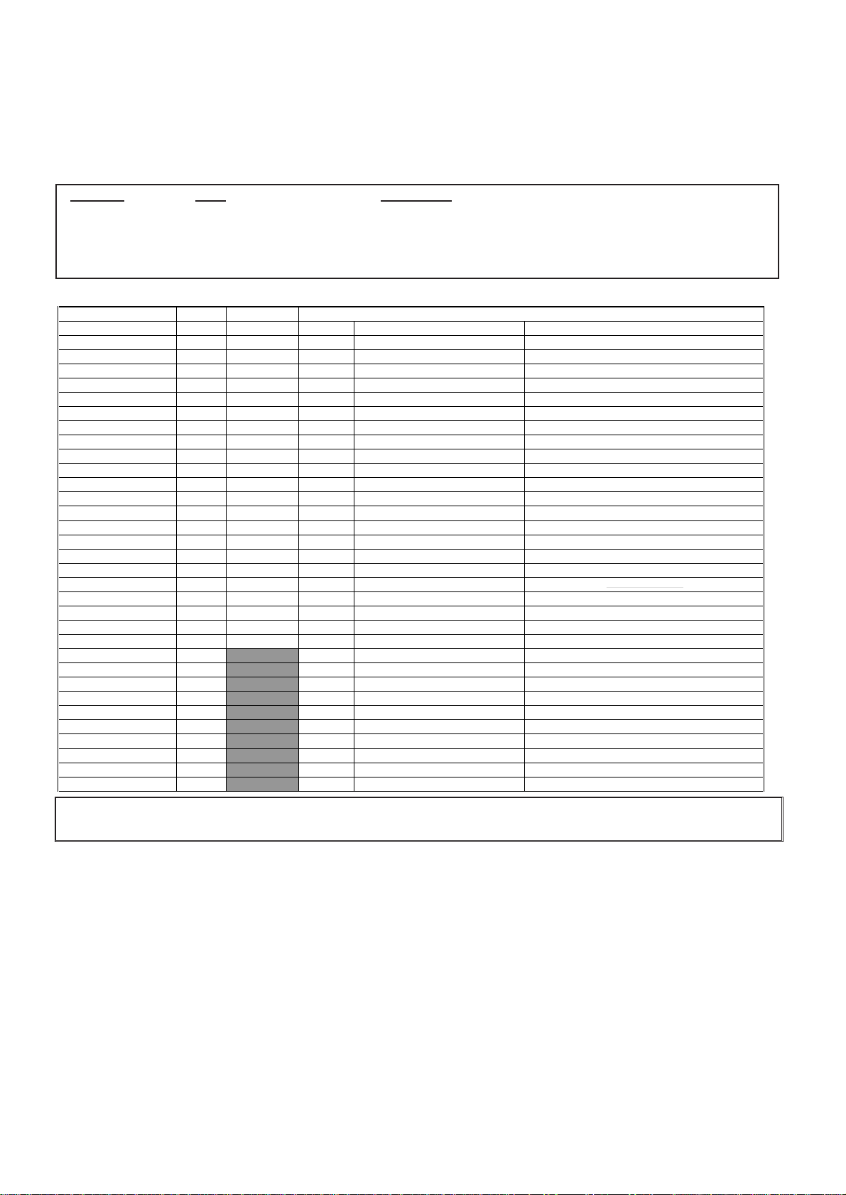
ADJUSTABLE SERVICE ADJUSTMENT
Service Item Number. Symbol 1 Symbol 2 Frequency Wide Mode
13 A01 Track. mode 50Hz Full Track. Mode(HCO)
14 A02 Vert. Zoom 50Hz Full Vertical zoom
15 A03 Vert. Slope 50Hz Full Vertical slope
16 A04 Vert. Shift 50Hz Full Vertical shift
17 A05 Vert. Ampl. 50Hz Full Vertical amplitude
18 A06 S-Corr. 50Hz Full S-correction
19 A07 V.Lin.Ctrl. 50Hz Full V.Lin.Ctrl.
20 A08 V.Linearity 50Hz Full V.Linearity
21 A09 EW Width 50Hz Full EW width
22 A10 Hor. Shift 50Hz Full Horizontal shift
23 A11 EW Parabola 50Hz Full EW parabola/width
24 A12 Trapezium 50Hz Full EW trapezium
25 A13 UC Parabola 50Hz Full EW upper corner parabola
26 A14 LC Parabola 50Hz Full EW lower corner parabola
27 A15 Hor. Bow 50Hz Full Horizontal bow
28 A16 Parallel 50Hz Full Horizontal parallelogram
29 A17 Vert. Scroll 50Hz Full Vertical Scroll
30 A18 H BLK SW 50Hz Full RGB blanking mode
31 A19 H BLK L 50Hz Full Timing of wide blanking front(WBF)
32 A20 H BLK R 50Hz Full Timing of wide blanking rear(WBR)
33 A21 OSVE 50Hz Full Black current measuring lines in overscan
34 A22 EVB 50Hz Full Extended vertical blanking
35 B02 Vert.Zoom 50Hz Natural / or 4:3 squeeze mode Vertical zoom
36 B09 EW Width 50Hz Natural / or 4:3 squeeze mode EW width
37 B10 Hor. Shift 50Hz Natural / or 4:3 squeeze mode Horizontal shift
38 B11 EW Parabola 50Hz Natural / or 4:3 squeeze mode EW parabola/width
39 B12 Trapezium 50Hz Natural / or 4:3 squeeze mode EW trapezium
40 B13 UC Parabola 50Hz Natural / or 4:3 squeeze mode EW upper corner parabola
41 B14 LC Parabola 50Hz Natural / or 4:3 squeeze mode EW lower corner parabola
42 B15 Hor. Bow 50Hz Natural / or 4:3 squeeze mode Horizontal bow
43 B16 Parallel 50Hz Natural / or 4:3 squeeze mode Horizontal parallelogram
44 B17 Vert.Scroll 50Hz Natural / or 4:3 squeeze mode Vertical Scroll
Explanation
Item No. OSD Description
7 VG2 Screen adjustment
151 WPR - N R - Drive adjustment
152 WPG - N G - Drive adjustment
304 AGC Take Over AGC adjustment
314 TXT - H - POS OSD Positioning adustment
IMPORTANT NOTICE
Do not attempt to adjust service adjustments not listed above otherwise it may cause loss of performance and product safety.
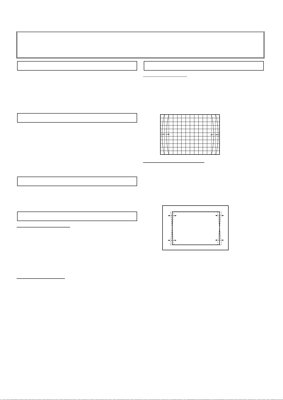
GEOMETRY SERVICE DATA

-7- C7WAS
To enter to the Service Mode
+ Press and hold the GREEN button on the remote control and then press the P▼button on the cabinet.
To select the service item and change data value
+ To select the adjustment item, use the P▲or P▼button.
+ To change the service data, use the Volume -(LEFT) or Volume + (RIGHT) button.
+ The data which is set in the service mode is stored into the memory IC automatically.
SERVICE MODE
SERVICE SERVICE SOFTWARE
ITEM ITEM VERSION
NUMBER DESCRIPTION
Exit from the Service Mode
+ Press the MENU button or turn off the TV set by using the Mains switch.
INITIALISATION OF MEMORY IC
To initialise the memory IC (IC801), press and hold the NORMAL button on the remote control, then press
the P▼button on the front panel of the TV set. The tv set will switch into standby mode. Turn the Mains switch Off
and On, then switch on from standby. The initialisation is now completed.
When initialised the memory IC and all of the setting data (option data and service adjustment data) stored in the IC
are reset to the default value. It is necessary to set the option settings and readjust the service adjustments listed in
this manual and to re-tune all the channels.
SERVICE
000 EB8A 3_52

-8-
C7WAS
ADJUSTMENTS
IMPORTANT NOTICE
Do not attempt to adjust the following service adjustments except when adjustments are required in servicing
otherwise it may cause loss of performance and product safety.
1. Receive white raster pattern.
2. Set controls to normal.
3. Connect digital voltmetre to test point TP-B and GND.
4. Adjust voltage to 150 ±0.5V by using VR641.
1. Input and tune an RF signal which is UHF to the clear-
est station.
2. Connect digital voltmetre to test point TP-A and GND.
4. Enter the service mode and select item no. 304. AGC
TAKE OVER
5. Press the LEVEL+ or LEVEL - button to adjust volt-
age to be 3.2Vdc.
By using FOCUS VR, adjust focus control for well
defined scanning lines.
SCREEN ADJUSTMENT
1. Receive black and white pattern.
2. Enter the service mode and select item no. 7. VG 2
3. Turn screen VR from min to max. OSD will change
from below to above. Turn back until below appears
and then stop turning.
DRIVE ADJUSTMENT
6. Select item no.151. WPR - N (R-Drive) or 152. WPG -
N (G-Drive) and adjust both initially to 20.
7. Change data value of each item by using LEVEL + or
LEVEL - button to obtain the proper white balance.
PCC ADJUSTMENT
1. Receive cross hatch pattern and set screen mode to
“FULL”.
2. Enter the service mode and select item no. 23. EW
PARABOLA
3. Press the LEVEL+ or LEVEL - button to adjust the
vertical line to be straight.
TRAPEZOID ADJUSTMENT
1. Receive cross hatch pattern and set screen mode to
“FULL”.
2. Enter the service mode and select item no. 24.
TRAPEZIUM
3. Press the LEVEL+ or LEVEL - button to correct the
trapezum distortion of the vertical line.
PCC ADJUSTMENT
GREY SCALE ADJUSTMENT
FOCUS ADJUSTMENT
AGC ADJUSTMENT
+ B VOLTAGE ADJUSTMENT

-9- C7WAS
CORNER ADJUSTMENT
1. Receive cross hatch pattern and set screen mode to
“FULL”.
2. Enter the service mode and select item no. 25. UC
PARABOLA for top corner adjustment OR item no.
26. LC PARABOLA for bottom corner adjustment.
3. Press the LEVEL+ or LEVEL - button to correct the
distortion of the vertical line around the corners.
HORIZONTAL CENTRING ADJUSTMENT
1. Receive circular pattern and set screen mode to
“FULL”.
2. Enter the service mode and select item no. 22. HOR.
SHIFT.
3. Press the LEVEL+ or LEVEL - button to adjust the
horizontal centre.
HORIZONTAL WIDTH ADJUSTMENT
1. Receive circular pattern and set screen mode to
“FULL”.
2. Enter to the service mode and select item 21. EW
WIDTH.
3. Press the LEVEL+ or LEVEL - button to adjust the
horizontal width.
1. Receive circular pattern and set screen mode to
“FULL”.
2. Set controls for brightness and contrast to maximum.
3. Connect high-voltage meter to the anode of CRT and
GND.
4. Confirm that voltage is 26 kV ±1.0kV at maximum
beam current 1.2mA ± 0.05
VERTICAL CENTRING ADJUSTMENT
1. Receive circular pattern and set screen mode to
“FULL”.
2. Enter the service mode and select item no.16.VERT
SHIFT.
.3 Press the LEVEL+ or LEVEL - button to adjust the
vertical centre.
VERTICAL HEIGHT ADJUSTMENT
1. Receive circular pattern and set screen mode to
“FULL”.
2. Enter the service mode and select item no. 17. VERT
AMPL.
3. Press the LEVEL+ or LEVEL - button to adjust the
vertical height.
1. Receive circular pattern and set screen mode to
“FULL”.
2. Enter the service mode and select item no. 314. TXT -
H - POS.
3. Press the LEVEL+ or LEVEL - button to adjust
proper OSD positioning.
OSD POSITIONING ADJUSTMENT
VERTICAL ADJUSTMENT
HIGH-VOLTAGE CONFIRMATION
HORIZONTAL ADJUSTMENT
314 TXT - H - POS 7

-10-
C7WAS
CPU PORT FUNCTIONS
Pin No Function Name Function In/Out
1 VSS Gnd --
2 VSS Gnd
3 1v8_1 1.8v Supply --
4 3v3 3.3v Supply --
5 Vref 3.3v Reference --
6 Vref V Ref Gnd --
7 Vref 3.3v Reference --
8 Vref V Ref Gnd --
9 Vref 3.3v Reference --
10 XTAL IN Clock Oscillator In
11 XTAL OUT Clock Oscillator Out
12 Vss Gnd --
13 Vguard sw --
14 Dec Dig 1.8v source supply Out
15 5v 5v Supply --
16 Phi 2 Phi 2 --
17 Phi 1 Phi 1 --
18 Gnd Gnd --
19 Sec pii --
20 Dec BG --
21 EW Drive parabola out Out
22 VdrB Vertical drive B Out
23 VdrA Vertical drive A Out
24 Vif 1 Vision IF 1 In
25 Vif 2 Vision IF 2 In
26 Vsc --
27 I Ref Reference current --
28 Gnd Gnd --
29 Sif 1 Sound IF 1 In
30 Sif 2 Sound IF 2 In
31 Agc Auto matic gain control In
32 Eht Eht In
33 SSif/Ref Iin/Avl/Ref Out --
34 Audio in Scart L In
35 Audio in Scart R In
36 Audio Out Scart L Out
37 Audio Out Scart R Out
38 --
39 Qsso/Amo/AudioEm --
40 Gnd --
41 PLL IF Phase Lock Loop If --
42 SifAgc SifAgc --
43 IFVo Scart 1 Video Out
44 FmRo --
45 V8Audio Switches --
46 AgcsSif --
47 V5P2 5v Supply --
48 Svo/IfVo/Cbvs1 Scart 2 Video Out
49 Audio4 L In Scart 2 Audio L In
50 Audio4 R In Scart 2 Audio R In
51 Y4/Cvbs4 Av3 Video In
52 C4 --
53 Audio2InL Av3 Audio L In
54 Audio2InR Av3 Audio R In
55 Cvbs2/y Scart 1 Video In
56 Audio3InL --
57 Audio3InR --
58 Y3/Cvbs Scart 2 Video In
59 C3 Scart 2 Chroma In In
60 Audio Out L SL Audio out Left Speaker Out
61 Audio Out L SR Audio Out Right Speaker Out
62 Audio Out HPL Scart Audio L Out 2 / monitor Out Out
63 Audio Out HPR Scart Audio R Out 2 / monitor Out Out
64 Pip --

-11- C7WAS
CPU PORT FUNCTIONS (continued)
Pin No Function Name Function In/Out
65 SVM Scan Velocity Modulation Out
66 FbiSo Flyback In SandCastle Out In/out
67 Hout Horizontal Drive Out Out
68 VssComb Gnd
69 V5Comb 5v Supply --
70 Vin/R2/Pr Scart 2 R-In In
71 Uin/B2/Pb Scart 2 B-In In
72 Yin/G2/Y Scart 2 G-In In
73 Y Sync Y Sync In
74 Y out Yout Out
75 Uout/Fb in Scart 2 Fast Blanking In
76 Vout/Sw01 --
77 Fbl3 Scart 1 Fast Blanking In
78 R3/Pr Scart 1 R-In In
79 G3/Y Scart 1 G-In In
80 B3/Pb Scart 1 B-In In
81 Gnd 3 Gnd --
82 V5P3 5vSupply --
83 BCL Beam Current Limiting In
84 Iblack --
85 Rout Red Drive Out
86 Gout Green Drive Out
87 Bout Blue Drive Out
88 V3.3A1 3.3v Supply --
89 RefAdn Ref Gnd --
90 V3.3RefAdp 3.3v Supply --
91 RefAd --
92 GndA Gnd --
93 V1.8A 1.8v Supply --
94 V3.3A2 3.3v Supply --
95 VssAdc Gnd --
96 V1.8Adc 1.8v Supply --
97 Into Remote control In In
98 P10/Int1 SCl In/out
99 P121/TO SDA In/out
100 V1.8C2 1.8v Supply --
101 VssC2 Gnd --
102 P04/I2Sws --
103 P03/I2SCLk --
104 P02/I2SDOC --
105 P01/I2SDOC --
106 P00/I2SDi1 StandBy Out
107 P13/T1 On/Off Out
108 P16/SCL SCL In/out
109 P17/SDA SDA In/out
110 V3.3P 3.3v Supply --
111 P20/Tpwm Relay On/Off Out
112 P21/Pwmo LED Drive Out
113 STATUS Status In/out
114 ALK Alk In/out
115 P30/Adco Scart 1 Pin8 Function In
116 P31/Adc1 Scart 2 Pin8 Function In
117 V1.8C1 1.8v Supply --
118 DecV1v8 1.8v Supply --
119 P32/Adc2 AGC In
120 P33/Adc2 Key scan in In
121 VssC1+P1 Gnd --
122 P24/Pwm3 Audio Mute Out
123 P25/Pwm4 L/L’switch (Export only) Out
124 V1.8C3 1.8v Supply --
125 Vssc3 Gnd --
126 P12/Int2 --
127 P14/Rx Power Fail In
128 P:15/Tx Natural Wide Switch

-12-
C7WAS
COMPONENT LOCATIONS
DANGER
LIVE MAINS
1
***
B10E3330A
DB=KG_PCB
CELL=B10E33300
17
31
1
5
8
EB8A
B10E33300
B10E3330B
***
A
A
A
C023
KF
KP
C104
C103
C102
C101
K1001
KEM2
TP-A
A101
K1003
K1002
KSC
T451
D610
IC601
R606
T611
R602A
C609
R607
T131
C1001
K1101
KCPA
KA
R614
K701
K7V
K7Y
R725
R742
R715
R705
K7Q
IC701
K7P
C710
Q461
R474
Q461-1
X201
X122
C214
X121
C229 C233
C236 C239
K3
K5
C256
C268
C271
C281
C283
C288
C203 C209
K4
C803
C210
C206
C205
Q202
IC801
C423 D441
Q451
C421
L441
C422
C424
T431
R433
C437
R451
R441
L442
L461
C451
L462
KQ
C486
C427
C426
C429
Q425
R477
C441
C443
C446
C434
R449
C466
3
K4A
Q432
C529
C502
C503
C501
R502
K4B
R512
R511
R515
R501
IC501
C010
C009
IC001
C022
J006
C667
C655
K2
Q642
C637
C686
D648
TP-B
C650
IC643
D642
IC641
VR641
C633
C642
C640
D630
D639
C643
D633
R667
C682
R648
R644
C841
C648
R637
D635
R435
C645
C685
R692
R691
IC666
KGG
JW1
JW2
KEM1
C691
R699
C481
JW3
JWA JWB
2
1
2
T4AH250V
T4AL250V
F601
PS601
L601
KE-2KE-1
KF-1
KF-2
L608
C601
F601-1 F601-2
KE
KFF
KF
C602
R601
D1911
A1901
SW1901 SW1902 SW1903 SW1904
RL601
D1901
KFF-1
KFF-2
SW601
VA601
12 21
KRKL
R031
KR-1
KR-2
K031
K1101
MAIN BOARD / FRONT BOARD / CRT BOARD

-13- C7WAS
IC BLOCK DIAGRAMS
IC001 LA42052 <Audio Output>
THERMAL PROTECTION CIRCUIT
OUTPUT AMPLIFIER
OUTPUT AMPLIFIER
INPUT AMPLIFIER
INPUT AMPLIFIER
REFERENCE
AMPLIFIER
3
2
12
6
5 7
4
PRE GND
IN 1
IN 2
1
RIPPLE FILTER
STAND BY
Vcc
8
10
P.P
RIPPLE FILTER
OUT 2
POWER
GND
OUT 1
POP NOISE PREVENTION BLOCK
IC501 LA78041 <Vertical Output>
THERMAL PROTECTION CIRCUIT
-
+
PUMP
UP
VER
OUTPUT
5
4
GND
PUMP UP
OUT
3
NON INV. INPUT
7
OUTPUT STAGE Vcc
6
Vcc
2
INVERTING
INPUT
1
AMPLIFIER

-14-
C7WAS
Internal power supply Input Under voltage protection
Oscillator
Falling edge detection
Burst On
Burst Off
Latch for Burst circuit
Logic
4
15
3
2
Block Diagram TN6Q03/04
Driver
Over current/FB comparator
Reference Voltage
Over voltage protection
Over heat protection Latch
Circuit
VDD pin
EDGE pin
FB pin SOURCE (GND) pin
DRAIN pin
IC601

-15- C7WAS

-16-
C7WAS
PIN DESCRIPTION OF SEMICONDUCTORS
A
K
C
BE
C2
C1
B1 B2
E
C
CBE
KA
C
B
E
B2
B1
C1 C2
E
E
B
C
B2
B1
C1 C2
E
B2
B1 C1
C2
E1
E2
K
AA
A
KK
K
A
K
A
C
BECBEC
B
E
1
2
3
4
5
6
Index
12N
Index Index
12N
2
13
(IN) (OUT)
(GND)
21 4
2
1
3
Index
1
N
Index 1
N
Index 1
N
Index 1
N
Index 1
N
Index
1N
2
131
232
1
3
RESET GND
Vdd
5
3
D
GSD
G
S
K: Cathode
A: Anode
C: Collector
B: Base
E: Emitter
D: Drain
G: Gate
S: Source
●Diode
●Transistor/FET
●IC
E1
C2
E2 C1
B2
B1
Index
●Diode
●Transistor/FET
●IC
FET

-17- C7WAS
PARTS DESCRIPTION AND READING IN SCHEMATIC DIAGRAM
1. The parts specification of resistors, capacitors and
coils are expressed in designated code. Please
check the parts description by the following code
table.
2. Some of transistors and diodes are indicated in
mark for the substitution of parts name. Please
check the parts name by the following code table.
3. Voltages and waveforms were taken with a video
colour bar signal(1Vp-p at 75 ohms terminated) and
controls to normal.
4. Voltages were taken with a high-impedance digital
voltmetre.
Example 2000 K K 1000 BG
Characteristic
Example 160 E M 10
Capacitance value
Tolerance
Type
Rated voltage
Excepting electric capacitors, all
capacitance values of less than 1
are expressed in µF and more
than 1 are in pF.
Example L2 C1 4R7 K N
Tolerance
Inductance value
Manufacture code
Unique code
Mark Material
E Electrolytic
P Electrolytic (non-Polarised)
C Ceramic (temperature compensation)
K Ceramic
F Polyester
N Polypropylene
M Metalised polypropylene
H Metalised polypromylar
B Ceramic (semiconductor)
G Metalised polyester
Y Composite film
S Styrol
T Tantalum oxide solid electrolytic
U Organic semiconductive electrolyte
D Electric double layer electrolytic
Mark Tolerance
A not specified
B ±0.1
C ±0.25
D ±0.5
F±1
G±2
E ±2.5
H±3
J±5
K±0
M±20
N±30
P +100 -0
Q +30 -10
T +50 -10
U +75 -10
V +20 -10
W +100 -10
X +40 -20
Y +150 -10
Z +80 -20
Mark Tolerance (nH) Mark Tolerance (%)
C ±0.25 G ±2
D ±0.5 J ±5
S ±0.3 K ±10
A ±0.2 L ±15
M±20
Coil Reading
Capacitor Reading
Example 1/2 D J 10K B
Example 6 W K 8.2
Example 1/2 C K 1M
Resistor Reading
Characteristic
Z (Carbon fuse)
B (Non-burnable)
Resistance value
Tolerance (see below table)
Material (see below table)
Rated wattage (W)
K indicates in KΩ
M indicate in MΩ
Note: Resistor which is indicated with resistance value only are
1/6W carbon resistor. Resistor which is indicated with materi-
al, tolerance and value are 1/4W rated wattage.
Mark Material
D Carbon
N Metal film
S Oxide metal film
C Solid
G Metal glaze
W Wire wounding or cement
H Ceramic
F Fusible
Mark Tolerance
A ±0.05
B ±0.1
C ±0.25
D ±0.5
F±1
G±2
J±5
K±10
M±20
P +5 -15
Z used in 0 ohm
●Material table ●Tolerance table
Mark Type number
-- 1S1555,1S2473,1S2076,1SS133,DS442,1SS176
K 1S1555,1S2473,1S2076,DS442
L 1S1555,1S2076A,1S2471
M 1SS133,1SS176,GMA01
N 1S1555,1S2473,1S2076,1SS133,DS442,1SS176,1N4148
P 1S1555,1S2076A,1S2471,1N4148
R 1S1555,1S2076,1S2473,DS442,1N4148
AA 1S1555,1S2076,1S2473,1SS133,DS442,1SS176,1N4148,GMA01
●Diode
Mark Type number
-- 2SC536 2SC945A 2SC1815 2SC1740 2SC1740S KSC945C
A E, F, G P, Q, R O, Y, G Q, R, S Q, R, S
B E, F, G P, Q, R O, Y, G Q, R, S
D F, G P, Q Y, G Q, R, S
F F, G P G R, S
H F, G P, Q Y, G Q, R, S Y, G
I E, F, G P, Q, R O, Y, G Q, R, S Y, G
G F, G P G R, S G
AD F, G Q, R Y, GR Q, R, S
AE E, F, G Q, R O, Y, GR Q, R, S
●Transistor (NPN type)
Mark Type number
-- 2SA608 2SA564A 2SA1015 2SA933 2SA933S KSA733C
Y E, F Q, R O, Y, G Q, R
WF R Y,GR
V E, F Q, R O, Y, G Q, R Y, G
U F R Y, G R G
Z E, F Q, R O, Y, G Q, R Q, R
AB F R Y Q, R
AE E, F Q, R O, Y R
●Transistor (PNP type)
Diode/Transistor Type Reading

-18-
C7WAS
CABINET PARTS LIST FOR MODEL CE28DN9-B-01
CABINET PARTS
1 610 310 7387 CABINET FRONT-C7WA
2 610 301 6665 BUTTON POWER-C6AA
3 610 301 6672 BUTTON UNITED-C6AA
4 610 310 7394 CABINET BACK C7WA
5 610 301 6689 DOOR-C6AA
6 665 000 2654 DEC IND-C7WA
7 610 253 2449 AC CORD HOLDER-U-D4VA
8 610 261 3032 COIL SPRING-E7GCS
9 645 043 5058 BADGE,SANYO*53.5X12L53.3
10 610 265 4202 HOLDER DC GBR-F3SC
ACCESSORIES
11 JXPLA RC TRANSMITTER
645 054 9533 BATTERY ENERGIZER R6SH2VP
665 000 2647 INST MANUAL - C7WA
665 000 2463 QUICK GUIDE - C7WA
Item Part No. Description
Note: Parts order must contain Service Ref. No., Part No., and descriptions.
11
JXPLB
9
1
328
5
6

C7WAS
-19-
CHASSIS ELECTRICAL PARTS LIST
Product safety should be considered when a component replacement is made in any area of a receiver.
Components indicated by a mark in this parts list and the circuit diagram show components whose value have
special significance to product safety. It is particularly recommended that only parts specified on the following
parts list be used for components replacement pointed out by the mark .
!
!
013C7WAS ELECTRICAL PARTS DIRECTOR
COIL
L901 645 060 9855 PRE-FORM,D-COIL,28-TOTOKU
PICTURE TUBE
Q901 414 012 4404 CRT A66QEW13X49 SAM BERL.
MISCELLANEOUS
SP901 652 000 0663 SPEAKER 8 OHM 3 WATT 5*9
SP902 652 000 0663 SPEAKER 8 OHM 3 WATT 5*9
W901 645 011 8838 3P AC CORD +2P HOUSE @2.1
W902 665 000 2159 GND CON.EB8A 28" 2P C7WLS
1AA0B10H0690A ASSY,PWB,MAIN C7WAS
CAPACITOR
C-R534 403 067 6274 POLYESTER 0.15U J 50V
C003 403 314 5915 GRM21BR71C474KA01L PT297
C004 403 314 5915 GRM21BR71C474KA01L PT297
C005 403 215 2310 GRM188R71H123KA01D PT115
C006 403 215 2310 GRM188R71H123KA01D PT115
C009 403 047 5065 ELECT 470U M 25V
C010 403 047 5065 ELECT 470U M 25V
C021 403 218 8101 ELECT 100U M 25V
C022 403 051 0627 ELECT 4.7U M 50V
C023 403 218 8151 25 YK 1000 M TA 1020
C030 403 113 3815 GRM188R71H102KA01D PT115
C031 403 086 3802 NP-ELECT 10U M 50V
C032 403 086 3802 NP-ELECT 10U M 50V
C033 403 215 2211 GRM188R71H103KA01D PT115
C034 403 215 2211 GRM188R71H103KA01D PT115
C035 403 215 2211 GRM188R71H103KA01D PT115
C036 403 215 2211 GRM188R71H103KA01D PT115
C040 403 113 4119 GRM188R71H222KA01D PT115
C057 403 113 3815 GRM188R71H102KA01D PT115
C1001 403 248 1618 16 YK 47 M TA 0511
C1003 403 157 3611 GRM1885C1H101JZ01D PT115
C1005 403 113 3815 GRM188R71H102KA01D PT115
C1006 403 157 3611 GRM1885C1H101JZ01D PT115
C1007 403 113 3815 GRM188R71H102KA01D PT115
C101 403 233 1111 ELECT 22U M 50V
C1011 403 248 1618 16 YK 47 M TA 0511
C1013 403 157 3611 GRM1885C1H101JZ01D PT115
C1014 403 157 3611 GRM1885C1H101JZ01D PT115
C1016 403 113 3815 GRM188R71H102KA01D PT115
C1017 403 113 3815 GRM188R71H102KA01D PT115
C102 403 039 3507 ELECT 470U M 6.3V
C1038 403 323 8815 GRM21BF51C225ZA01K PT115
C1039 403 323 8815 GRM21BF51C225ZA01K PT115
C104 403 233 0817 ELECT 10U M 50V
C106 403 215 2211 GRM188R71H103KA01D PT115
C107 403 215 2211 GRM188R71H103KA01D PT115
!
!
!
!
!
Ref. No. Part No. Description
Chassis construction
CE28DN9-B-01
013C7WAS ELECTRICAL PARTS DIRECTOR (PAGE 19)
1AA0B10H0690A ASSY,PWB,MAIN C7WAS (PAGE 19-24)
1AA0B10H0690B ASSY,PWB,SOCKET C7WAS (PAGE 24)
Read description in the Capacitor and Resistor as follows:
CAPACITOR
CERAMIC 100P K 50V
Tolerance Symbols:
Less than 10PF
A: Not specified B: ±0.1PF C: ±0.25PF
D: ±0.5PF F: ±1PF G:±2PF
R: ±0.25-0PF S: ±0-0.25PF E: +0-1PF
More than 10PF
A: Not specified B: ±0.1% C: ±0.25%
D: ±0.5% F: ±1% G:±2%
H: ±3% J: ±5% K: ±10%
L: ±15% M: ±20% N: ±30%
P: +100-0% Q: +30-10% T: +50-10%
U: +75-10% V: +20-10% W:+100-10%
X: +40-20% Y: +150-10% Z: +80-20%
Material:
CERAMIC............Ceramic
MT-PAPER ..........Metallized Paper
POLYESTER ......Polyester
MT-POLYEST......Metallized Polyester
POLYPRO............Polypropylene
MT-POLYPRO ....Metallized Polypropylene
COMPO FILM......Composite film
MT-COMPO ........Metallized Composite
STYRENE............Styrene
TA-SOLID ............Tantalum Solid
AL-SOLID............Aluminium Solid
ELECT ................Electrolytic
NP-ELECT ..........Non-polarised Electrolytic
OS-SOLID ..........Aluminium Solid with Organic Semiconductive Electrolytic
DL-ELECT ..........Double Layered Electrolytic
RESISTOR
CARBON 4.7K J A 1/4W Rated Wattage
Performance Symbols:
A: General B: Non flammable Z: Low noise
Other: Temperature coefficient
Tolerance Symbols:
A: ±0.05% B: ±0.1% C:±0.25% D: ±0.5%
F: ±1% G:±2% J: ±5% K: ±10%
M:±20% P: +5-15%
Rated value, ohms:
K: 1,000, M: 1,000,000
Material:
CARBON ............Carbon
MT-FILM ..............Metal Film
OXIDE-MT ..........Oxide Metal Film
SOLID..................Composition
MT-GLAZE ..........Metal Glaze
WIRE WOUND ....Wire Wound
CERAMIC RES....Ceramic
FUSIBLE RES ....Fusible
Rated Voltage
Rated value: P=pico farad, U=Micro farad
Note: Parts order must contain Service Ref. No., Part No., and descriptions.
Other manuals for CE25DN9-B
1
Table of contents
Other Sanyo TV manuals

Sanyo
Sanyo C14ZA25 User manual

Sanyo
Sanyo DP26746 - 26" LCD TV Instruction Manual

Sanyo
Sanyo CPP3002 User manual

Sanyo
Sanyo CP29KX2 User manual

Sanyo
Sanyo CE28D6-C User manual

Sanyo
Sanyo CE14AT3-GB User manual

Sanyo
Sanyo CT29FS1 User manual

Sanyo
Sanyo DP32640 - 31.5" Diagonal LCD HDTV 720p User manual

Sanyo
Sanyo 21D2 User manual

Sanyo
Sanyo 25BN1 User manual

Sanyo
Sanyo LCD-39XR12F User manual

Sanyo
Sanyo AVM-3650G User manual

Sanyo
Sanyo CE32FWH2F-C User manual

Sanyo
Sanyo CE15LC3-B User manual

Sanyo
Sanyo CP14SA1 User manual

Sanyo
Sanyo CE25DN3-B User manual

Sanyo
Sanyo CP29YS2B User manual

Sanyo
Sanyo CP14KX2A User manual

Sanyo
Sanyo C21LF37 User manual

Sanyo
Sanyo CP29AF2X User manual