-10-
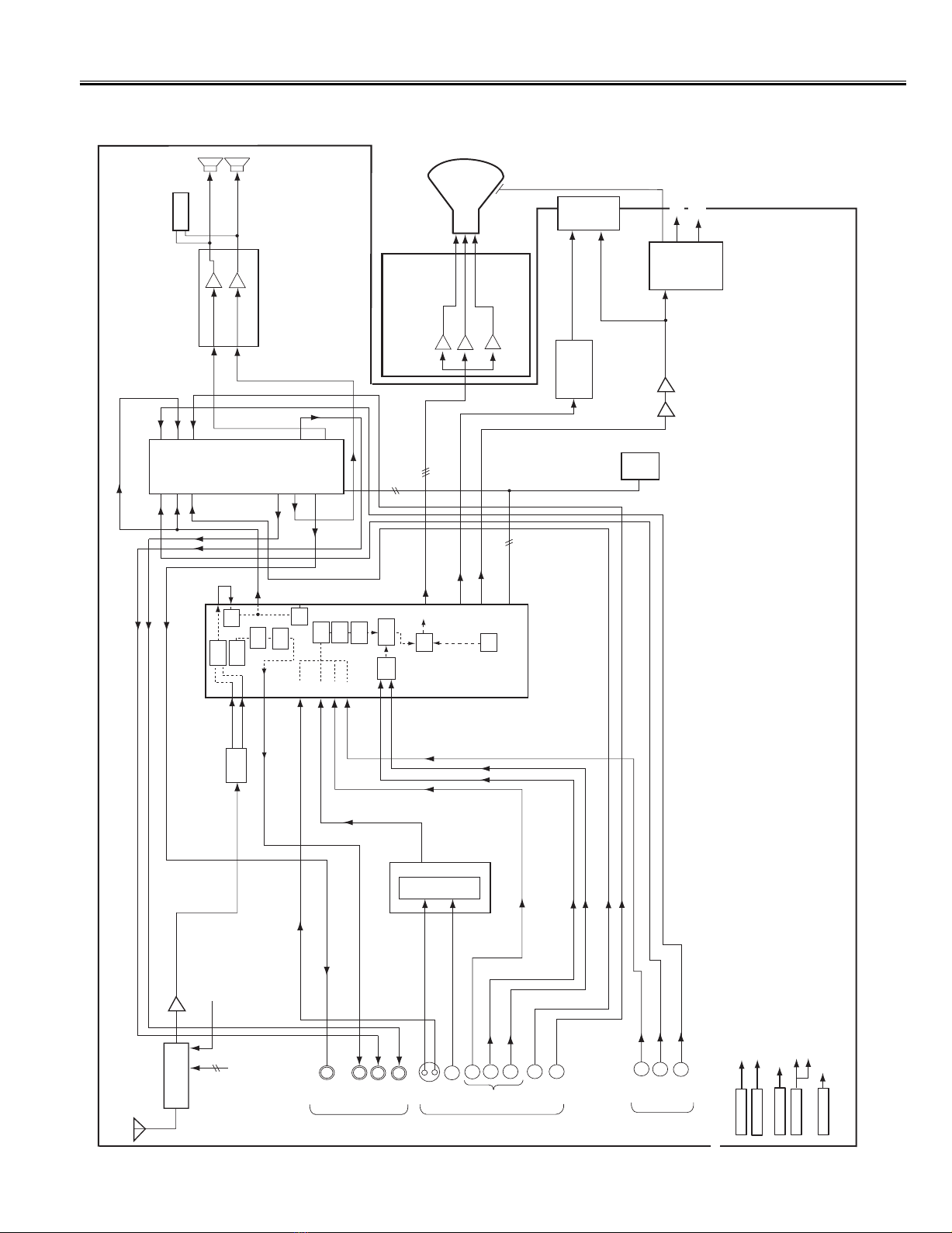
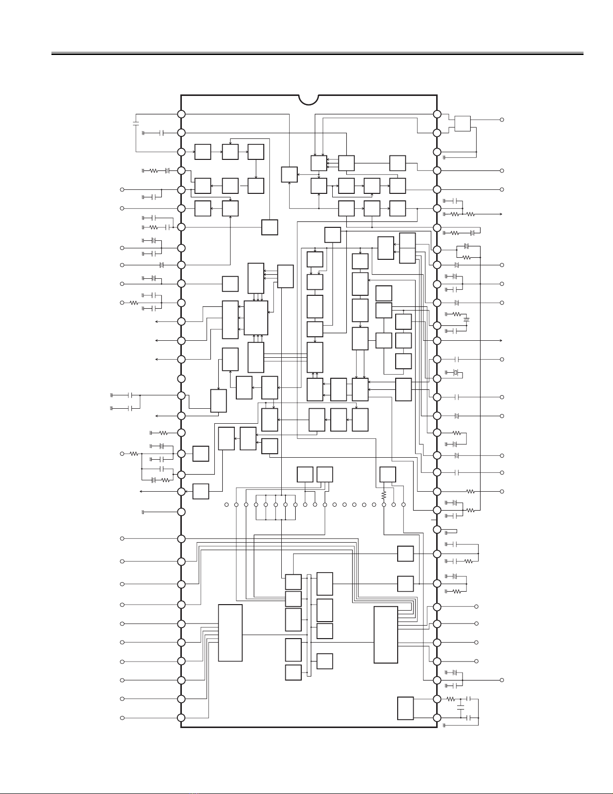
Service Adjustments with Replacing Memory IC(IC801)
(/JE0187C)
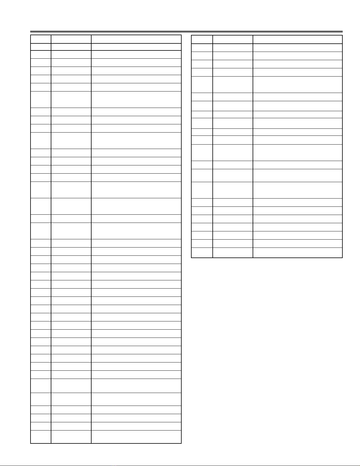
DATA INITIAL
No. ITEM RANGE SETUP DESCRIPTION
DATA
01 RFAGC 0~63 27 RF AGC Adj.
02 H-PHA 0~31 10 H-Phase (H-Centering) Adj. (50Hz)
03 V-POS 0~63 40
V-Position (V-Centering) Adj. (50Hz)Fixed.
04 V-SHIFT 0~15 3 V-Phase Adj. (50Hz)
05 V-SIZ 0~127 35 V-Size Adj. (50Hz)
06 V-LIN 0~31 17 V-Linearity Adj. (50Hz)
07 V-SCO
0~31
15 Vertical S-Correction Adj. (50Hz)
08 V-TRANS
0~1
0 Data transmission between V Retrace
09 V-RES 0~1 0 Vertical Reset Timing.
10 H-P60 -16~+15 +3 H-Phase Adj. (60Hz) difference val.
11 V-S60 -64~+63 +1 V-size Adj. (60Hz) difference val.
12 V-SHIF60 -16~+15 -3 V-Phase Adj. (60Hz) difference val.
13 OSDHP 0~255 23 OSD H-Position Adj.
14 OSDC 0~7 4 OSD Contrast Adj.
15 V-SCP 0~7 7 V-Size COMP Adj.
16 H-SCP 0~7 7 H-Size COMP Adj.
17 EWDC 0~63 36 H-Width / H-Size adj.
18 EWAMP 0~63 7 EW Parabola / Width ratio
19 EWTILT 0~63 40 EW Trapezium correction
20 EWTOP 0~15 9 EW Corner Top
21 EWBTM 0~15 9 EW Corner Bottom
22 EWCNRSW 0~3 0 Select control range for corner corr.
23 EWTEST 0~7 0 Select EW DAC test mode
24 EWDC60 -
32~+31
+1 H-Width / H-Size Adj. NTSC (60Hz)
25 EWAMP60 -
32~+31
0 EW Parabola/Width ratio NTSC (60 Hz)
26 EWTILT60 -
32~+31
+1 EW Trapezium correction NTSC (60 Hz)
27 EWTOP60 -
16~+15
0 EW Corner Top NTSC (60Hz)
28 EWBTM60 -
16~+15
0 EW Corner bottom NTSC (60Hz)
29 SBIAS 0~255 105
Sub Bias Adj.
30 RBIAS 0~255 0
Red Bias Adj.
31 GBIAS 0~255 0 Green Bias Adj.
32 BBIAS
0~255
0 Blue Bias Adj.
33 RDRIV
0~127
64 Red Drive Adj.
34 GDRIV 0~15 8 Green Drive Adj.
35 BDRIV 0~127 64 Blue Drive Adj.
36 1 Line Appear White Balance Adj.
37 DRV White Balance Adj.
38 B-YD 0~31 27 B-Y DC Level
39 R-YD 0~31 25 R-Y DC Level
40 B-YDN -16~+15 0 NTSC B-Y DC Level Adj.
41 R-YDN -16~+15 0 NTSC R-Y DC Level Adj.
42 SBDC -16~+15 -5 SECAM B-Y DC Level Adj.
43 SRDC -16~+15 -2 SECAM R-Y DC Level Adj.
44 B-YDD -16~+15 -14 DVD B-Y DC Level
45 R-YDD -16~+15 -17 DVD R-Y DC Level
Following table shows the initial values which have been stored in the CPU ROM, and items for the service adjustments.
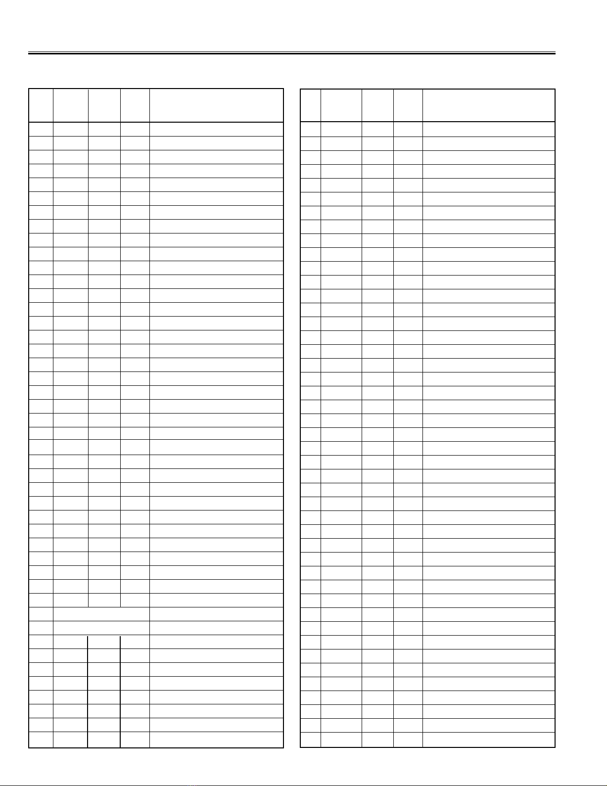
Service mode adjustments table in CPU ROM
DATA INITIAL
No. ITEM RANGE SETUP DESCRIPTION
DATA
46 RGBTEMP 0~1 0 RGB Temp. SW
47 RGBTEST 0~1 0 RGB Test
48 EXTRGBC 0~1 0 External RGB Contrast
49 RGBTEST 0~1 0 RGB Test
50 HALFTONE 0 ~ 3 0 Halftone Color
51 G-YA 0~1 0 G-Y Angle
52 GYAMP 0~15 8 G-Y Amplitude Adj.
53 RBGB 0~15 8 R-Y / B-Y Gain Balance
54 RBAG 0~15 8 R-Y / B-Y Angle
55 G-YAN 0~1 0 NTSC G-Y Angle
56 GYAMPN -8~+7 0 NTSC G-Y Amplitude Adj.
57 RBGBN -16~+15 0 NTSC R-Y / B-Y Gain Balance
58 RBAGN -16~+15 0 NTSC R-Y / B-Y Angle
59 RBGBDN -16~+15 +10 DVD NTSC R-Y / B-Y Gain Balance
60 RBAGDN -16~+15 -5 DVD NTSC R-Y / B-Y Angle
61 VOLFIL 0~1 0 DAC Volume filter disable
62 APCOFFSET 0~1 0 Align APC Offset Current
63 IF-AGC 0~1 0 IF AGC defeat
64 OVERMOD 0~1 0 Select Over Modulation Circuit Type
65 COGV 0~3 1 Coring Gain
66 BLKS 0~3 3 Blk. Str. Start (w/ defeat)
67 BLKG 0~3 3 Blk. Str. Gain
68 BRTA 0~1 0 Brt. Abl. Def.
69 BRST 0~1 0 Mid. Stp. Def.
70 BRTH 0~7 0 Bright Abl. Treshold
71 WPL 0~3 2 White Peak Limit Op. Point (w/ defeat)
72 YGAM 0~3 0 Y Gamma Start
73 PRS 0~3 0 Pre-shoot AV Adj.
74 ORS 0~3 2 Over-shoot AV Adj.
75 DCREST 0~3 0 Select Luminance DC Restoration
76 RFCO 0~3 2 RF Coring Gain Difference
77 PRSN 0~3 0 Pre-shoot RF Adj.
78 ORSN 0~3 2 Over-shoot RF Adj.
79 CTRAP 0~7 4 Chroma Trap control
80 CBPF 0~3 0 Chroma BPF control
81 CBPFN 0~3 1 Chroma BPF control NTSC
82 CBPFAVN 0~3 0 Chroma BPF control AV NTSC
83 TINT -16~+15 0 Tint RF
84 TINT443 -16~+15 +4 Tint (NTSC4.43)
85 SHRF -32~+31 0 RF Sharpness
86 SH Adj -32~+31 0 Sharpness Adjustment
87 COL TEST 0~1 0 Color Test
88 COL NTSC -32~+31 -20 Color NTSC (difference from PAL)
89 CODP -16~+15 -10 DVD PAL Color
90 CODN -16~+15 -15 DVD NTSC Color