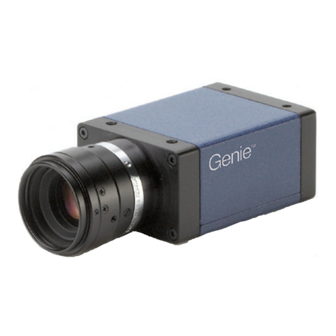
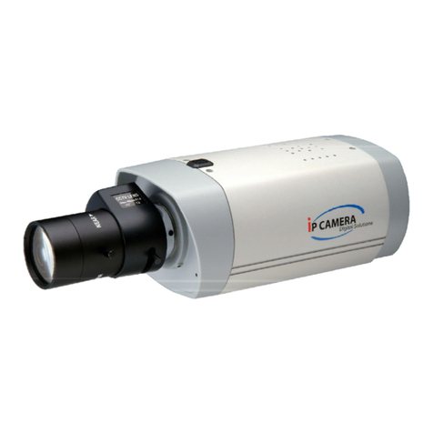
SenTech STC-GE33OX User manual

No.11S098-03
1
STC-GE33OX/GEC33OX
Users guide Rev. 1.03
Sentech Power Plus
VGA Color / Monochrome CCD
GigE Vision Camera
STC-GE33OX
STC-GEC33OX
Users guide
Sentech Co., Ltd

No.11S098-03
2
STC-GE33OX/GEC33OX
Users guide Rev. 1.03
Revisions
Rev
Date
Changes
Note
1.00
2011/08/29
New document
1.01
2012/01/31
Update
Change, add and delete the camera control commands
Add the strobeSignal for the output signal
Change the GenICam command / Camera command reference table
1.02
2012/04/12
Update
Update the GenICam command / Camera command reference table
1.03
2017/04/17
Update
Address, TEL, FAX number for relocation

No.11S098-03
3
STC-GE33OX/GEC33OX
Users guide Rev. 1.03
Contents
1The connector specifications......................................................................................................................................... 6
1.1. RJ45 connector .............................................................................................................................................................. 6
1.2. Power/IO connector........................................................................................................................................................ 7
1.2.1 Input signal ............................................................................................................................................................... 8
1.2.2 Output signals........................................................................................................................................................... 8
1.3. DC IRIS lens connector.................................................................................................................................................. 9
2I/O circuits ...................................................................................................................................................................... 10
2.1 Input circuit.................................................................................................................................................................... 10
2.2 Output circuit ................................................................................................................................................................. 12
3User configurable FPGA (XILINX) ................................................................................................................................ 13
3.1 User configurable FPGA (XILINX) information.........................................................................................................13
3.1.1 Device information............................................................................................................................................. 13
3.1.2 User program examples....................................................................................................................................13
3.2 Block diagram and explanation ................................................................................................................................ 14
3.2.1 Block Diagram................................................................................................................................................... 14
3.2.2 Explanations of data flows ................................................................................................................................15
3.2.3 Important design consideration of data timing and handling............................................................................. 24
3.3 Connection information between the devices .......................................................................................................... 25
3.3.1 Connection between the user configurable FPGA (XILINX) and the Sentech FPGA.......................................25
3.3.2 Connection between user configurable FPGA (XILINX) and DDR2 ................................................................. 27
3.3.3 Connection between the user configurable FPGA (XILINX) and the EEPROM ...............................................28
3.4 Development guideline.............................................................................................................................................29
3.4.1 Module and constraints files..............................................................................................................................29
3.4.2 Important design cautions.................................................................................................................................29
3.4.3 Notice for use DDR2 memory...........................................................................................................................30
3.4.4 Recommend the image data handle between the Sentech FPGA and the user configurable FPGA............... 31
3.4.5 Copy guard function..........................................................................................................................................31
3.4.6 Schematics of the user configurable FPGA (XILINX) .......................................................................................31
4The camera output timing charts................................................................................................................................. 32
4.1 The horizontal timing................................................................................................................................................ 32
4.1.1 Color Bayer order (This information is only for STC-GEC33OX)......................................................................32
4.2 The vertical timing .................................................................................................................................................... 33
4.2.1 Full scanning..................................................................................................................................................... 33
4.2.2 AOI .................................................................................................................................................................... 34
4.3 The transferring image ............................................................................................................................................. 35

No.11S098-03
4
STC-GE33OX/GEC33OX
Users guide Rev. 1.03
5Camera function modes................................................................................................................................................ 36
5.1 Normal mode............................................................................................................................................................ 36
5.2 Pulse width trigger mode.......................................................................................................................................... 37
5.2.1 Timing................................................................................................................................................................37
5.2.2 Exposure timing with the positive polarity trigger signal ...................................................................................38
5.2.3 Exposure timing with the negative polarity trigger signal.................................................................................. 38
5.3 Edge preset trigger mode.........................................................................................................................................39
5.3.1 Timing................................................................................................................................................................39
5.3.2 Exposure timing with the positive polarity trigger signal ...................................................................................40
5.3.3 Exposure timing with the negative polarity trigger signal..................................................................................40
5.4 Edge preset trigger mode (The trigger input while the image is out) ....................................................................... 41
5.4.1 Timing................................................................................................................................................................41
5.4.2 Exposure timing with the positive polarity trigger signal ...................................................................................42
5.4.3 Exposure timing with the negative polarity trigger signal.................................................................................. 42
5.5 H reset mode............................................................................................................................................................ 43
6The communication protocol specifications .............................................................................................................. 44
6.1 The communication method.....................................................................................................................................44
6.2 The communication settings..................................................................................................................................... 44
6.3 The communication format....................................................................................................................................... 45
6.4 The camera control commands................................................................................................................................47
6.4.1 The camera control commands list................................................................................................................... 47
6.4.2 Description of the camera control commands (Device code: 000000) .............................................................50
6.4.3 Description of the camera control commands (Device code: 100000) .............................................................59
6.4.4 Sequence for the command saves to the EEPROM.........................................................................................70
6.5 GenICam command / Camera command reference table .......................................................................................71

No.11S098-03
5
STC-GE33OX/GEC33OX
Users guide Rev. 1.03
This document is the connectivity and operation users guide for
STC-GE33OX/GEC33OX.

No.11S098-03
6
STC-GE33OX/GEC33OX
Users guide Rev. 1.03
1 The connector specifications
1.1. RJ45 connector
Caution: This product is a PoE type. Apply power (+10.8 to 26.4Vdc) through the power/IO connector when PoE is
not supported.
Pin assignment
Note. Power supply connection comprise PoE (IEEE802.3af).
LED information
Power ON the camera Green LED: Blinking
1Gb transferring
Yellow LED: OFF, Green LED: Blinking 100Mb transferring
NIC, HUB or LAN cable is not support 1Gb. Please use 1Gb supported NIC, HUB and LAN cable.
Please check the NIC and HUB setting is “1Gb transferring” when use with 1Gb supported NIC and
HUB.
When snapping of the CAT5e cable, possibility to change the transferring speed from 1Gb to 100Mb.
Please change the CAT5e cable.
Pin No. Signal name
1
TA+
2
TA-
3
TB+
4 TC+
5
TC-
6 TB-
7
TD+
8 TD-
Yellow LED Green LED Status
Orange light ON Green light ON
Power ON
Orange light ON
Green light blinking 1Gb transfering
Light OFF
Green light blinking 100Mb transfering

No.11S098-03
7
STC-GE33OX/GEC33OX
Users guide Rev. 1.03
1.2. Power/IO connector Connector: HR10A-10R-12PB (Hirose) or equivalent.
This connector is for DC power input and the input and output signals.
Pin assignment
Note.1: All I/Os (Pin number 3 through 10) are user assignable.
Note.2: DO NOT connect or disconnect the power/IO connector while the power input though PoE.
No. Signal type IO direction Spec. Initial signal
1 POWER IN GND - GND -
2 POWER IN - +10.8 to 26.4Vdc -
3 OUT0_AUX_OP OUT Opt. Isolated FrametriggerWait out
4 OUT1_AUX_OP OUT Opt. Isolated ExposureActive out
5 OUT2_AUX_OP OUT Opt. Isolated Open
6 OUT3_AUX_OP OUT Opt. Isolated Open
7 OUT4_AUX_OP OUT Opt. Isolated Open
8 IN0_AUX_OP IN Opt. Isolated TRG In
9 IN1_AUX_OP IN Opt. Isolated Open
10 IN2_AUX_OP IN Opt. Isolated Open
11 IO VCC IN - IO VCC -
+3 to +26.4Vdc
12 IO GND - IO GND -
Refer Fig. 3
12pin connector

No.11S098-03
8
STC-GE33OX/GEC33OX
Users guide Rev. 1.03
1.2.1 Input signal
TRG IN: Input the trigger signal
High: Voltage of the “IO VCC IN”
Low: Smaller than 0.4V
1.2.2 Output signals
Set the output signals from the power/IO connector.
The following six output signals are selectable with the software or communication.
A) FrameTriggerWait
The user can check the camera conditions, which are the camera expose and the image output
processing by the trigger signal with this FrameTriggerWait signal.
a) High status (Voltage of the “IO VCC IN”): No processing by the trigger signal
The camera accepts the trigger signal
b) Low status (0V): The camera is expose and the image output processing by
the trigger signal
The camera default setting is the input trigger signal is INVALID while low status for this signal.
When the exposure starts while the image output by next trigger signal, please change the camera setting
(Device code: 00H, Command: 13H) to accept the trigger signal while the image output.
The noise appears on the image when start exposure while the image output. In this case, please change
the “H reset”for the exposure start mode (Device code: 00H, Command: 12H) to change the exposure
start point to next HD timing.
B) UserOutput
The status of this UserOutput signal can change with the “UserOutputValue”.
C) ExposureActive
The user can check the exposure time with this ExposureActive signal.
a) High status (Voltage of the “IO VCC IN”): The camera is exposing
b) Low status (0V): The camera is not expose
D) TriggerAuxiliary
This TriggerAuxiliary signal is the input trigger signal.
E) TriggerInternal
This TrigerInternal signal is the input trigger signal with the trigger delay time.
F) SensorReadOut
This SensorReadOut signal is the FVAL signal, which is the image output period of the time.
G) StrobeSignal
The StrobeSignal signal is the strobe control signal.

No.11S098-03
9
STC-GE33OX/GEC33OX
Users guide Rev. 1.03
1.3. DC IRIS lens connector
Connector: M1951 (EMUDEN) or equivalent.
Pin assignment
1 2
3 4
Pin No. Signal name
1
DAMP-
2
DAMP+
3
DRIVE+
4 DRIVE-

No.11S098-03
10
STC-GE33OX/GEC33OX
Users guide Rev. 1.03
2 I/O circuits
2.1 Input circuit
Response timing
Input circuits
CAMERA
Response time
11[ns]
11[ns]
11[ns]
11[ns]
Tf
520[ns]
545[ns]
584[ns]
689[ns]
Ts
100[ns]
100 [ns]
100[ns]
100[ns]
Tr
3.0[us]
3.0[us]
2.8 [us]
2.5[us]
Td
24[V]
12[V]
5.0[V]
3.3[V]
IO_VCC
10%
90%
Td
Ts
Tr
Tf
USER INPUT
INPUT
OPTO ISOLATOR
SHARP:PC400J00000F
IO_VCC
CAM_VCC
If
INPUT
USER_INPUT
Maximum consumption of If is 6 mA

No.11S098-03
11
STC-GE33OX/GEC33OX
Users guide Rev. 1.03
Example circuit for the input signal
USER_INPUT
OPTO ISOLATOR
SHARP:PC400J00000F
IO_VCC
CAMERA
CAM_VCC
IO_GND
If
INPUT
OPTO ISOLATOR
SHARP:PC400J00000F
IO_VCC
CAMERA
CAM_VCC
IO_GND
If
INPUT
IO_VCC
USER_INPUT

No.11S098-03
12
STC-GE33OX/GEC33OX
Users guide Rev. 1.03
2.2 Output circuit
Response timing
Output circuits
OPTO ISOLATOR
SHARP PC354NJ0000F
IO_VCC
USER_OUTPUT
OUTPUT
IO_GND
10k Ohm
CAMERA
Ts
Td
10%
90%
Tr
Tf
OUTPUT
USER_OUTPUT
Response time
10.9[us]
6.9[us]
3.8[us]
3.1[us]
Tf
2.8[us]
2.8[us]
2.2[us]
2.2[us]
Ts
31.0[us]
42.3[us]
60.2[us]
67.5[us]
Tr
28.4[us]
35.2[us]
30.4 [us]
29.6[us]
Td
24[V]
12[V]
5.0[V]
3.3[V]
IO_VCC

No.11S098-03
13
STC-GE33OX/GEC33OX
Users guide Rev. 1.03
3 User configurable FPGA (XILINX)
The customer would program the provided FPGA (XILINX) with its own proprietary code and the customer would
also have complete control over the “Memory”utilization.
Sentech checks the camera for proper operation by “Disabling”around the customer’s code and memory control.
3.1 User configurable FPGA (XILINX) information
3.1.1 Device information
The manufacturer names and item numbers of the user configurable FPGA and the peripheral devices are
listed in the table-1.
3.1.2 User program examples
Implementation of proprietary algorithm
Image processing and conversion
Image storage
Image analysis
Pattern comparison and others
Device Part number Size Manufacture
FPGA XC3SD1800A (Package: CSG484) 1800 k gate XILINX
DDR2 W9725G6JB-25 32 MB Winbond
EEPROM M95512-RMN6TP 512 kbit ST Micro
Configuration ROM M25P80-VMP6G 8 Mbit Micron
(Table-1) FPGA and the peripheral devices

No.11S098-03
14
STC-GE33OX/GEC33OX
Users guide Rev. 1.03
3.2 Block diagram and explanation
3.2.1 Block Diagram
CCD CDS/AD Sentech
FPGA
Gig-E
I/F
User configuration
FPGA (XILINX)
Camera
Gigabit-
Ethernet
port
DDR2
Memory
(32MB)
Image data
UART User configuration
FPGA (XILINX) area
Configuration
SPI BUS
EEPROM
(512Kbit)
Configuration
ROM (8Mbit)
12bit image data
Clock/FVAL/LVAL
25MHz
Power/IO
connector
JTAG
connector
3 inputs
5 outputs
JTAG
(TCK, TMS, TDI, TDO)
I/O
JTAG
Fig.1 Block diagram

No.11S098-03
15
STC-GE33OX/GEC33OX
Users guide Rev. 1.03
3.2.2 Explanations of data flows
3.2.2.1 Image data
3.2.2.1.1 Image data flow
1) The analog image signal created by the CCD is processed through CDS (Correlated Double Sampling)
section and then is converted into digital data by the A/D converter.
2) This data is sent to "Sentech FPGA" for further processing.
3) Once the data is sent into "Sentech FPGA", the image data can be routed to "User Configurable FPGA".
Three different extraction points are provided in "Sentech FPGA" for this purpose. Please see
Section-3.2.2.1.2-2) for more details.
4) This data is further processed by the program you create in "User Configurable FPGA".
5) Now, the data should be returned to "Sentech FPGA". In this process, again, three different points are
provided in "Sentech FPGA" to return the data to. Please see Section-3.2.2.1.1. 3) for more details.
6) The data is sent to "GigE I/F (Interface)" and sent out through the Ethernet connector.

No.11S098-03
16
STC-GE33OX/GEC33OX
Users guide Rev. 1.03
3.2.2.1.2 Image data extraction and insertion
The image data generated by the CCD is converted into 12-bit digital data as the section 3.2.2.1.1
explained. Then this data is extracted into the user FPGA, processed and inserted back to Sentech
FPGA.
1) Image data flow block diagram
CCD CDS/AD
Sentech
FPGA
User configurable
FPGA (XILINX)
DIN0 - 11
White
Balance Gamma Color
Interpolation
The image data from Sentech FPGA to user configurable FPGA
A B C
Sentech
FPGA
User configurable
FPGA (XILINX)
DOUT0 - 11
White
Balance Gamma Color
Interpolation
The image data from user configurable FPGA to Sentch FPGA
CBA
Fig. 2 Image data flow block diagram

No.11S098-03
17
STC-GE33OX/GEC33OX
Users guide Rev. 1.03
2) Data extraction from Sentech FGPA
The 12-bit image data is extracted from Sentech FPGA as DIN11-0 into the user FPGA from any points
listed below. These points A, B and C are indicated in fig.2 (Image data flow block diagram).
A) For the color camera
A. CCD raw data
B. Data after the white balance processing
C. Data after the white balance and the gamma processing
B) For the color camera
A or B. CCD raw data
C. Data after the gamma processing
3) Data extraction from user configurable FGPA
After processing the 12-bit image data in the user FPGA, the data is inserted back to the Sentech FPGA
as DOUT11-0 at any points listed below. These points A, B and C are, again, indicated in fig.2 (Image
data flow block diagram).
A) For the color camera:
A. Before the white balance, the gamma and color interpolation processing
B. Before the gamma and the color interpolation processing
C. Before the color interpolation processing
B) For the monochrome camera
A or B Before the gamma processing
C Before the output from the camera (No processing)
4) Data assignment list
Please see section 3.3 for the data assignment.
It is not necessary to consider these data pin assignments if use the pin assignment and the timing
constraints file (Power_plus_000.ucf).

No.11S098-03
18
STC-GE33OX/GEC33OX
Users guide Rev. 1.03
5) Image data switching method
As explained in the section 3.2.2.1.2, there are three points to extract out the image data from the
Sentech FPGA and the image process at Sentech FPGA after the image data send back from the user
configurable FPGA. There are two different methods to achieve this switching.
A) By using Sentech GUI “StCamGigEWare_OpDemo”
Also please see User configurable FPGA (XILINX) Sample Codes.
a) Select “OP Setting”under “Option”in the menu.
b) Select which image data sends from “Sentech FPGA”to “User configurable FPGA”at
“Sentech FPGA -> User FPGA”
c) Select the image process at Sentech FPGA after the image data send back from “User configurable
FPGA”at “Process after User FPGA -> Sentech FPGA”
Selection
Color camera Monochrome camera
CCD data CCD raw data CCD raw data
White balance processed data White balance processed image data CCD raw data
White balance and White balance processed and Gamma processed image data
gamma processed data gamma processed image data
Image data from Sentech FPGA
Selection
Color camera Monochrome camera
No process No image data from the User FPGA No image data from the User FPGA
White balance, gamma and White balance, gamma and Gamma processing
color interpolation color interpolation processing
Gamma and color interpolation Gamma and color interpolation processing Gamma processing
Color interpolation color interpolation processing No processing
Image process at Sentech FPGA after the image data send back from User FPGA
(Table-2) Image data selection from Sentech FPGA
(Table-3) Image process at Sentech FPGA

No.11S098-03
19
STC-GE33OX/GEC33OX
Users guide Rev. 1.03
B) By changing the register value through the UART
Also please see section “6 The communication protocol specifications”.
a) Set the image data between FPGAs (Device code: 20H, command: C0H).

No.11S098-03
20
STC-GE33OX/GEC33OX
Users guide Rev. 1.03
3.2.2.2 Configuration data
1) The FPGA program created by users is sent to "Configuration ROM" through the Ethernet connector as
"Configuration data".
2) The data is sent through "GigE I/F" and "Sentech FPGA" to "Configuration ROM" and stored.
(Note) Please see “User configurable FPGA (XILINX) uploading instructions”for more detailed
information.
3) Select “Enable”at “User FPGA Enable”when the user configurable FPGA has to configure with the
uploaded configure data for the user configurable FPGA.
The user configurable FPGA does not work if select “Disable”at “User FPGA Enable”.
A) By using Sentech GUI “StCamGigEWare_OpDemo”
Also please see User configurable FPGA (XILINX) Sample Codes.
a) Select “OP Setting”under “Option”in the menu.
b) Select which image data sends from “Sentech FPGA”to “User configurable FPGA”at
“Sentech FPGA -> User FPGA”
B) By changing the register value through the UART
Also please see section “6 The communication protocol specifications”.
a) Set 01H for the “Use FPGA Enable”(Device code: 20H, command: 19H).
This manual suits for next models
1
Table of contents
Other SenTech Security Camera manuals
SenTech
SenTech STC-CL500E User manual
SenTech
SenTech STC-400 Series User manual
SenTech
SenTech STC-1100C User manual

SenTech
SenTech STC-GE83A User manual

SenTech
SenTech STC-A33A User manual

SenTech
SenTech STC-C42A Owner's manual

SenTech
SenTech STC-TB83USB-ASH User manual
SenTech
SenTech STC-SCS231POE Installation instructions
SenTech
SenTech STC-400 Series User manual
