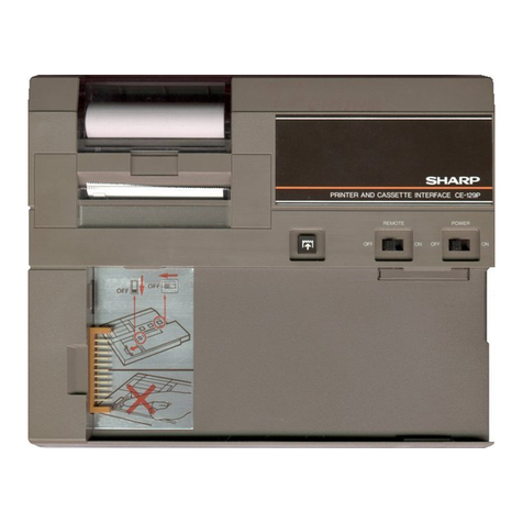
Sharp CE-126P User manual

-
SHARP
-
CE 126P
SERVICE MANUAL
• PRODUCTS OUTLINE
rhe CE-126P prlnter is an optional printer with the cassette
'nterface designed for use with the pocket computer models
?C-17"''', PC-1250, PC-1251, and PC-1401 (El-55OOI.
~.SliECIFICATIONS
'rinter type:
'rinting positions:
'rint speed:
)aper feed speed:
~ecording paper:
~ 'ower supply:
'owe......_.,nsumption:
3attery Iife:
Oot matrix thermal printer (MTP-
201 I, identical to the one used for
the CE-125
24 printing positions
Approx. 0.8 Iines/second
Approx. 0.8 lines/second
CPAPR1025CC05 (EA1250P, identi-
cal to the one used for the CE-1251
Thermal recording paper (paper roll
with outer diameter of 18 mm, maxi-
mum, and width of 58mml
Uses four UM3 (AAl dry celJ batter-
ies.
Options:
AC adaptor (EA-23EI
NiCd battery (EA-27BI
EA-23E for rechargel
3 watts
UM3:
SUM3:
EA-27B:
(use of the
Approx. 2000 lines
Approx. 3000 lines
Approx. 5000 lines
(recharge time: about 15
hours)
'hysical dimensions: 140.5(WI x 116(01 x 23(HI mm
3. TAPE RECORDER INTERFACING
METHOD
CE-l26P
Tape Recorder, etc.
Pocket computer
PC-12SO, PC-1251,
PC-1251 H, PC-1245,
PC-1401, etc,
CODE:OOZCE126PSM/E
MODEL CE-126P
G,..,
pi",
tfOfc!llU
=7:!:.~~
I•
I !:'•
Mika it
connected
I • I
;:t:
!At::'ONE
<,
SPEAKER jock 01
the
upe
recorder.
Grav plug
Ifor
datl
transfer
.nd ....rifiation'
Rod
pi",
(tor recording)
• Use of the CE-125 Tape Recorder exclusively design'ed
for the Pocket Computer is recommended.
C-tt. Tape Recorder
The following is a descriptlon of the minimum tape recorder specifi-
cations necessary for interfacing with the CE-l26P.
Item Requirements
1. Recorder Type Any tape recorder, standard
cassette or micro-casserte
recorder, may be used in accor-
dance with the requirements
outlined below.
2. Input Jeck The recorder should have
11
mini-jack input labeled "MIC".
Never use the "AUX" jack.
3. Input Impedance The input jack should be a low
impedance input (200 - 1,000
OHM.)
4. Minimum Input level Below 3 mV or -SO dB.
5. Output jack Should be a minijack labeled
"EXT. (EXTernal speaker",
"MONITOR", "EAR (EAR.
phone" or quivalent.
6. Output impedance Should be below 10 OHM.
7. Output level Should be above 1V (practical
maximum outpur above 100
mW)
8. Distortion Should be within 15% within a
range of 2 kHz through 4 kHz.
9. Wow and Fluner 0.3% maximum (W.R.M.S)
10. Other Recorder motor should not
fluctuate speed.
L...__
SHARP CORPORATION
Do not sale !

CEl26P
NOTES:
• Some of tape recorders may not operate properly owing
to different specification or electrical characteristics
affected by signal distortion, electrical noise, level drop-
out caused after long years of use.
• When using the tape recorder fitted with the mixing
feature, it needs to disable the mixing function for both
recording and playback.
• Depending on the tape recorder used, better reading
result may be attained when the red plug is unplugged
from the MIC jack.
• As
it
may impede proper data transfer and verif'lCation
depending on the position of the volume control, tone
control, bass contral, and treble controI, try to find the
optimum level by varying their positions.
4. CIRCUIT DESCRIPTION
The CE-126P has two microprocessors; the P-CPU by which
data traosfer is carried out with the host CPU (M-CPU) and
the printer control PCU. Since the host CPU (PC-1245,
1250, 1251, 1401, (EL5500) have different CPU actions,
the CE-126P CPU therefore performs different action.
M-CPU to P-CPU data transfer method (for PC-1245, 1250,
1251)
, OEYICE SELECT,
SELI
~:
B"'SY~
_r-u---'
:10)_ ..... _. ~
,,---
.
,
.
ACL ' ACL
ACK~
.
PCU1t"".
DWT
~'f'-----
4-1.
What action should the P-CPU take prior to data transfer is
dependent on thestate of SEL1 and SEL2 from the M-CPU.
(DEVICE SELECT)
4-2.
SEL1 SEL2 Action
L L Nop
LHPCU select
HLRemote ON
HHACl
The following actions take place before data transfer.
(1) SEL 1 goes low and SEL2 high.
(2) BUSY trom the M-CPUturns high level.
(3) Upon receipt of BUSY, ACK of the P-CPU is set high
and the data is received to the p·CPU.
Since the data
is
transferred in bit by bit serial mode,
above steps (2) and (3) are repeated eight times to complete
transfer of one data. For instance, those steps are repeated
for 192 times (24 x 8) in order to transfer a 24 digits data.
The print command, however, is sent out to the P-CPU at
the end of the data in a form of the code "00"
4-3.
M-CPU to P-CPU data transfer method (for PC-1401,
EL5500)
Since there are no SEL1 and SEL2 used for the PC·1401
and EL5500, DEVICE SELECT is dependent on the
contents of data.
(UEYlca SELECT)
SOUT
_j, ~ __.
= ....._........__
J
t
:~ ;--V"\
L
DOUT
(1) For DEVICE SELECT, XOUT becomes high.
(2)
As
the P-CPU receives a high state of XOUT, it sends
ACK to the M-CPU.
(3)
As
the M-CPU receives ACK, it sends back BUSY.
(4) Oata is received to the P-CPU with a high state of
BUSY. ACL, REMOTE ON, CPU select actions is
carried out depending on the contents of data.
4-4. Print data transfer
(DATA 11IAHSPORTATlOH)
SOUT
IIlJSY
__.,f!_._.IL_,
ACI! /\
I
~
I.
Bl1'1I1I
:~
XOUT goes low when the print data is transferred. Data
transfer
is
done in a manner identical to those of the PC-
1250.
-2-
Do not sale !

5.BLOCK DIAGRAM
e
6.CPU(UPD7506G515
SIGNAL DESCRIPTI
CE 12S-P
liREMOTEl
lIT ... t2 F.AR
circuit
Xi" ~
Low battery
I
X01II ~IIIC
1'21 P63
PI!
P23
Basy
PI3
CPU
P22
Dout Pli
DiD PSI
P2I)
ACK P62
PS)
POIl POl
P53
SELI
f
J
SEL2
DI-4 R/'WIlJSYSEL
1
HI-1
IDF PCU
T
TI
I
PD
Driver I. C
Zero-

R
Crass
I.C
HI-1
11
T
)
PRINTER
ON
Pin No. Signal Name ln/Out Description
P03 SEL2 In Select
POO SEL1 In Select
P13 BUSY In Handshake, active high
P12 XOUT In Device select, active high
Pll DOUT In Data, active high
Pl0 DOUT In Printer error
P23 ACL/SEL1 Out Hilt!: ACL Low: nomal
P22 CS/SEL2 Out Hilt!: chip select Low: non-select
P21 REM02 Out Remote off
__r---L
Remote off pulse generation
.20 RIW Out High: read, "High to low transition: write
P43 PIS In Data transfer mode
Hi!ta: parallel Low: serial
P42 NORMAL PAPERI In PCU select
THERMAL PAPER High: normal paper PCU Low: thermal paper PCU
P41 LOWBATTERY In Low banery check
High: normal Low: low battery
-
P40 ACK In Handshake (PCU to printer CPU)
P53 03 ln/Out Dm line between CPU and PCU MSB (High ..•..• 1, Low ..••.• 0)
P52 02
InlOut
Data line between CPU and PCU (High •...•• 1, Low ...... 0)
P51 01 InlOut Dm line between CPU and PCU (High ...... 1, Low .....• 0)
,
P50 00
InlOut
Data-line between CPU and PCU LSB (High •...•. 1, Low ..•... 0)
I
P63 REM01 Out Remote on ~ Remote on pulse generation
P62 ACK Out Handshake (to host CPU), active high
P61 OIN Out Printer error (to host CPU)
High: printer error low: nonnal I
P60 BUSY Out Handshake (printer CPU to PCU), active high
-3-
Do not sale !

-
-
CE 126P
7. PCU (SC6994) SIGNAL DESCRIPTION
Pin No. Signal Name In/Out Oescription
1SEL2 In Select
2SEL1 In Select
3
VOO Out Power supply
4ACl Not used
5 BUSY In Hi!tl: chip select - - - - - - • - - low: Non-select
6
AIW
In Hi!tl: read High to low transition: write
7-10 04-1 In Oata input
11 STP Not used
12 S In Oata transfer mode select line
High: serial input - - - - - - - - low: parallel inputloutput
13 24 In Print digit select line
High: 24 digits (GNO connected) low: 16 digits
14 10F Out Printer motor drive signal
I
15 H7 Out Printhead elernent on pulse
I
16 H6 Out Printhead element on pulse
17 GNO In Power supply
18-22 H5- H1 Out Printhead element on pulse
23
A
In Printer reset (printhead home position detect)
24
PD
Out Power down (in supply during printer operating cycJe, otherwise,
power is not supplied to the printer drive circuit.
25 TIn Printer timing (generated frorn the tachogenerator of the motor)
26-28 TSl-3 In Test pins
29 VP1 Out Printer control circuit supply power
30-32 BC1-3 In/Out PCU frequency control
33 CCK Out Clock test pin
34 HA In
35 HB Not used (Print density adjust pin ... JA and JB pin connection
varies according to the printhead rank).
36 HC In
37,38 Cl1,2 In Basic cJock pulse control resistor fitting pin
39 PF In Paper feed key input
40 NP In GN0 Connected
41 ACl In All cJear input
42 OP3 Out ACL select (high when on)
43 OP2 Not used.
44 OP1 Not used.
-4-
Do not sale !

-
8. SERVICE CAUTIONS
8-1. Cautions in exchanging the printer unit
Inorder to prevent print density variation caused by
thermal head resistance variation, the printhead is classified
into three ranks of A, B, and C, and the rank is indicated
on the reverse side of the printer unit F.P.C. After exchange
of the printer unit, relevant circuit change must be observed
in accordance with the procedure mentioned below.
Short JA when the rank A printer is used.
Leave all open when the rank B printer is used.
Short JC when the rank C printer is used.
8-2. Threading lead wires
o
Laad
wire A
@
-
CE 126P
After the above procedure, adjust by means of the 20-
Kohms protentiometer so that an optimum print quality is
obtained. The circuit has been so designed as to attain the
best result with the potentiometer set at its midway.
Therefore, existence of a remarkable print density variation
might involve the following problems:
1. Drop in head performance
2. Ouality change in the thermal recording paper
3. Throuble in the thermal control circuit
• 'o'e
sure to observe the following cautions in installing
lead wire.
* 1,* 2: The lead wire A most be threaded under the
cotton wire and fixed on the F.P.C. using the
adhesive tape.
*3: The lead wire B should be fixed with the adhesive
tape along the rib of the bottom cabinet,
8-3. ~ Installing PWB
(1) Set the lead wire to the given location of the ~ PWB
and solder it.
(2)
As
shown in the figure, apply the double tack adhesive
tape over the CPU (UP07506G) on the
0
PWB, then
set the
@J
PWBover it with the hole facing the relay.
(3) After the installation of the
@]
PWB, solder the lead
wire to the
@]
PWB.
8-4. Connecting ~ with [[]
As shown in the figure, fix the 13-pin F.P.C. with the
cotton wire. The cotton wire also has to be soldered in a
same manner as the F.P.C.
*4:
00
not allow the strayed lead wire and solder to
extend out of the Ni-Cd battery terminal to the
printer unit, when the 'lead wire is being soldered
to the NiCd battery terminal.
(
Unless lead wires A and Bare threaded properly, it may)
cause to recharge the dry battery (UM3 or AA) because
of slack lead wires, when the AC adaptor is used with
dry batteries in installation. .
F.P.C. 13
pin
(Hold the midway part)
-5-
Do not sale !

-
CE 126P
9. PARTS
&
SIGNALS POSITION
...--------------------------------------00
PWB (Top and
bottl
Chip dl ..... DAN202
-
.
..
i:
PI
-
Co)
.:
..:
AC I.PI
@]
PWB (Top view)
J
EG
ltI -
I,F
3
A18U x4
470Knt
C.Ir C
BE"
f.
B E H
1Mn
58Kn
...
E
1,F
L
KF
":r~
.(1
·C
.(1
-Q
••C
-Q
'.. Q
-ca
-ca
-ca
\
-6-
Do not sale !

:rn vievv
> ___
tom .Iew)
1
POWER SW
--------------
I'O~'I
I .
1
!
l " .
J
:1
'uH -;_
~ • __./ lfI
Cl
~~ " ..../"'4)~
· .:,/'"/-."_-~U·~
--
~"
.
"r..-
11
I:..
~'OKII .\.'
,! .
-;:::_r"R ........
1
'l -.
I ~
_y~_; __
., ~ AII7.-; ~ .' .,'- •
o
·-~3-1 ..
-'--.-i.___
··,·t
1-- - - - - - - -
I Printer INd wir. - - - - ..,
---
I
--=,.
I
-=l:c:~
I
~!!!.!
cl':
!ci
ff r~
:;JJJ
i]1
Chi, tranilitor ,a", code Tr name
M.
ranll
RH-IXIOIOCCNI AI171 M8,
Mi
RH-IX1012CCNl C2.12
Li. LI
RH-IX 100lCCNl
8
.15
••:Bi
RH-IXIOO4CCNI AI03. HP,HQ.HR
RH-TXI01SCCNI 01044 X8 , Xl
Do not sale !

10.
CIRCUIT DIAGRAM
@I
PWB
Trltt'(ZSCI_
All .. _ .......
i.
ZSCIC8I
E
Q
;llIn
EI IG~
Iy
470Kn"2
D
e
a
L
100
.Kn
100KI\
I~i•.
,lOH
DAP401
PWB .
UXZ,.......-l)l-
2ZKn
i ;;..;
21111<RVR ....
i'~
10 2llKAVR
i
ZSC2811
3
4
Illn
100Kft
I 0,
ICIIKn
10Kft
Priala'
1Iad-.....
"NlectiCII
[!J
pwa
REIIOTI! S.
47ft
"'ICIIPP
""
I
I
pp'
- --'-+-------,
I
I
l
-1
6
P_ leodKEY
I
1
L
(PCU)
5C6994
- - - - -- -+--t
r-l-+-I-
~
O-el"
,J
1
I
RE
I
~
I 1
1
I
UKft :
r
lZ I
tr.!.z_-,-
ZSD~
l!AIt
IIIC
~
A
M,...
-rJ1Jll1J
M'"
~HHH
881n
4.7Kn
Ittn
:0,1"
.~
IOttn
..... DAN •
~
4.71(11
••
(CPUI
:-ttl'-!1
L+_':' __ ~
..
Dout
100Kn
Xia
~,
T
Xout
....-_
Din
G'
HI
ACK
I'
J\
SELZ
I I I I
I
I I
I
111
SELI
10Kn
Block
reOi....
2a1I<nIc4"2
IOOPF 111
2
11
_..-trt-tlt!
_._..__..Lt_t
.fJ
Block
resistor
22OKnx4
-7-
Do not sale !

!fl
~'."9."
.,.
.
M51Zl1L
EJ
...,
---..
-
~
VR
2SA
1179
IKn
~i~~t
*
IGV
4~r
Tr:i
.-.
a,
1..-1
H COIOlON
r---...,
iI
1
i
,_
---+
I
1
.
-
II
III
-0
..
I
1
.
~
11~:5
~! :
H7
-0
I
I
L___
J
GND
unq
IIGEIN
)i.
U
~U_ Ni--cd
I
L--
_J
Printer IITP20I-Z41lA
LI"I
.
......_
HZ8BLL
--1_-- __ -,
I
I
I
I
I
I
I
I
I
~_S.
I ,...-----.
V I
o-f
I
I
I
I
t>I
I
I
22n
.
-"""
T
•• lipiD
_tor
cable
r--- ---
~Rewtl .
llad
!:alte" :
ON
IIfTOU1'I
~l!j(SIIJ bh.,>
GND~
XiD
IVa
(Bh.>
<>_f;"
.GND
.a('i .. )
fU?!
(Purph,j
"0-
X ... ,
lOOK""!
SELI
1iC!!(Br ..... )
I.
VGG
SELI "'C!! (Rod)
BUSY
lIIC!!(BIac:k)
Daut af!.(White)
Dia
.f!I(Yell_)
ACk
fQ<!l
(0.......,)
.VGG ~i!l(Gt1I,.)
•
T
I I
VI;';
•
CE 1261'
+
Do not sale !

-
CE126P
11. PARTS LIST &GUIDE
rn
Exteriors
(*.IU.~~)
NO. PARTS CODE
PIlICE RANK
NEW
PAIIT
r
DESCRIPTION
Ja
Ex
MARK
RAHIl
1 GCOVA1363CCZZ OF AO
0
.....:.,.t
'11",:
Paper cover
2 PCUT 102SCCZZ
00
AC
0
......:, ,-t
'IJ~,'
Paper cutter
3 GCABB2761CCZZ OS AG
N
0
"''I"t''''.x. TODcabinet
4 JKNBZ122SCCOI DA AA C
~.f -,
+ SW
"'7::
Silde switch knob
S QCNTMI042CCZZ DA AA C ~7-fYSW:::I:'-'7~ Slide switch terminal
6 JKNBZI877CCOl OK AE C
'"
~,7'
Kev top (Paper leed kev)
7 PGUMM1337CCZZ OB AB B
~1.~7"J;'-7'
Rubber spring
8 QCNW-12 6 8CCZZ FG AT
N
C
11PIN
:1*7'-
.,.-7''''
11
Pin connector cable
9 TCAUK1217CCZZ DA AA
N
0
f'.2."'of 7"'" Caution label CJapanese
&
Englisl!l_
10 PHOG-1093CCZZ OC AB 0
11
t,";.- :1
*
7
'-"'-7'/"3'"
Rubber cap lor llpin connector cable
~1.lf:1"'77'
11
XUBS020P04DDD DA AA C
t'~
Screw
12 PSLDC143DCCZZ 00 AC C
;, -IV
y,~;,-
Shield
13 Q T ANZ 1 4 S 4 C C Z Z OB AB C'1';.-+',/;' Battery terminal
(6)
14 GC ABA 2 7 6 2 CC Z Z OS AG
0
"''I"t'"I:::I Bottom cabinet
IS G F TAB 1 18 9 C C D1 OD AC
0
'1':.-+
7'
Batterv lid
16 P C US S 1 2 2 7 C C Z Z DA AA
N
C'1';.-+~"".x.3'"
"';'3;;
Cushion
17 QTANZl186CCZZ DA AA B'1';.-+';.-:'- Batterv terminal
(E!7)
18 GLEGGIOIICCZZ DA AA B
~1.7;'
Rubber
le2
19 XUB S F 2 6 P 1 D0 0 D DA AA C
1:"~
Screw
20 LX-BZlI20CCII DA AA C
t'~
Screw
I
21 QCNTMI062CCZZ OB AB
N
C
':",11 1"3"'" 1"'"
Ni-Cd terminal
22 QCNTFI061CCZZ OB AB
N
C
':"111 1"3'"
:17-{ Ni- Cd tenninal
23 PSHEPII08CCZI DA AA
N
CSL SW 117:.--1' SL SW spacer
24 P C U SG 1 2 2 8 CC Z Z DA AA
N
C
7,,11
'-f""7~1.
Rubber cushion
2S PCUSS1218CCII DA AA C
7'1)
;;'-3'"
Printer cushion
26 Ki-OBOO8ICCZI HL BG E
""-71\.7'1)/,-
Thermal printer unit CMTP-201)
27 jlCNCW13 21 CCD 3 DJ AE B :1*7'-
SPIN
Connector 5pin_twith lead wire}
L_
L.
------ - --- -
III
PWB unit
(~~.:l.='~
t-)
NO. PARTS CODE
PAICE RANK
HEW
PAIIT
DESCRIPTION
Ja
Ex
MARK
RANK
1 PRDARI035CCZZ OE AC
N
B
*..,
*';I'~;;
Heat sink
2 PTPEH1224CCII DA AA N C:17-f7
7'
Adhesived tape (for C-PWB)
3 QCNCW13D8CCAi OE AC B
""-7"'7'1
1;; '-FPC
3;
*
7'- Connector lor printer (Spin Black)
4 QCNCII1323CCDF OB AG B :1*7'- Connector (Spin Blue)
5 QCNW-12 7
8CCII
OE AC
N
B
F,P.C.
F.P,C. (l3pin)
6 QJAKCIDD3CCZZ DH AD B91"-,7 Jack (Ior AC adaptor)
7 QJAKCID13CCZI DO AC C9'1"77 Jack (Ior MICEAR)
8 QJAKCIOl6CCIZ OH AC B 91"
'1
7Jack (Ior Remote)
9 QSW-SD07SFCII DL AF B~7-{
Y;t.-f
-,f' Slide switch
10 VCTYPUINXI04M OB AB C :1:.-'1'/"" Capacitor (12WV O.IOJlFl
11
RC-EZI08BCC1A OE AC C:1;'-'1';'-""- CaPilcitor ClOV1000uFl
12 RC-E Z4 7 7 ACC 1A 00 AC C:::1;;'1';'-""- Capacitor (lOV 470pFl
13
RC SZ10D7CCZZ OL AF C :1;'-"';'-"" Capacitor (luFl
14 RC-SZ1D21CCZZ OE AC C:1/'1';'-""- Capacitor ClOWV3,3uFl
15 RH-iXIOI0CCII OC AB B
~7/9;t.'-
Transistor (Al179 M6)
,
16 RH-TX 10 1SCCIZ 00 AC B
~7;;;;;7.'
Transistor (DI048,X6 x7)
17 RH-TXI 0
16CCI I
00 AC B
~7/;;;t.'-
Transistor CC16S2-PQR)
18 RMPTC4224QCKB OY AK C
7'0·,
77-f:1'" Block resistor
(1/8W
220Kn x 4 + 10%)
19 RRLYZ2400QCZZ EN AP B
I)
v
Relav
20 RVR-M2415QCZZ DF AO B
;f,
1)..,1.
Variable resistor
21 YCKYPUIHB101K DA AA C:1/'1'/""- Capacitor CSOWV100pfl
22 VHDDS158812 1 OB AB B
Y.f
~-I'
Diode CDSI588L2)
23 VHD1SS108//-1 OB AB BY-f
~-r
Diode
24 VHD1IE1N///-l OB AB
B
Y-f ~-
r
Diode (lOEIN)
25 VHEHZ3BLl// 1 00 AC B
"':..1'
Y-f~
I'
Zener diode
26 VHERD6.2E9/ 1 OB AB B
''/:..1'
Y-f:t
I'
Zener diode
27 VHiDAP201//-1 OE AC B Yof:t
1'7H
Diode arrav
28 VHiDAP40l//1 DQ AE B
Y{~-Y7H
Diode array
29
VHiLB1256MFPI EA AK
B
IC
IC
30
VHiM5123L//-1
OS
AG
B
IC
IC MS123L
31 VHiUPA66H//-1 DL AF
8
Yoft
Y7"-f
Diode arrav
32 VRD-ST2BYI02J DA AA C7{:1'" Resistor Cl/8W l.OKn
+
5%)
33 VRD-ST2BY103J DA AA C7{:1'" Resistor (l/SW 10Kn ±5%)
34
VRD-ST2BY104J DA AA Cf{:1'" Resistor
(1/8W
100Kn +S%)
35
VRD ST2BY683J DA AA C7of:1'" Resistor Cl/SW 68Kn +S%)
36
VRD-S T 2E Y39 1 J OB AA
C
1]-;j{/7{
:1'"
Resistor
(l/4W
3900 ±S%)
37 VRD ST2HY8R2J DA AA C7-{:1'" Resistor
Cl/2W
8.2n +5%)
38
VS2SCl162-CDC DL AE B
~7/;;1..'-
Transistor
39 XBBSD26PD6000 DA AA
C
1:'1..
Screw
40
RC CII021CCN1 OB AB C:1/'1'/"" Capacitor (O.luFl
41 RC CZI031CCN1 OB AB C:1/1'/""- Capacitor ClOOOPF)
42 RC-CZI035CCNl OB AB C:1/1'/""- Capacitor ClOOpFl
43 RC CZI039CCNl
08
AB C :::1;,<1';,<"" Capacit9! (470011El
-- - ---
Do not sale !

,-
--
-
-
,
NO PARTS CODE
PRICE RANK NEW PART
0 E S C R I P T ION
. Ja Ex MARKRANK
44
RC-CZI052CCNl OB AB C :1:'-7':.-"'- Capacitor(lSOpF)
45 RH-OZI008CCNl
00
AC B '>('1'-1'71..-{ Diodearray(DAN202)
46
RH-iXI004CCNl OH AO B
~7:.-:;~1-
Transistor {AI036)
47 RH-iXI009CCNl
00
AC B
~7:'-:;~1-
Transistor(BSISB6B7l
48
RH-iXI010CCNI OD AC B
~7:.-;;~1-
Transistor (All
79 M6)
49 RH i X I 0 I 2 C CN 1 D
0
A C B ~
7:'- :;
x
I
Transistor (C2812,L5 l6)
50
RR KZI051CCNl DA AA C
r>(:1'"
Resistor(220KO+2%)
51 RR-KZI053CCNl DA AA C
r>(:1'"
Resistor_(I20KO±2")
52 RR-KZI066CCNl DA AA C
r{:1'"
Resistor(20KO+2")
53 RR-KZI067CCNl DA AA C
r>(:1'"
ResistorClSKO±2")
54
VH i 07 5 0 6 G- 5 1 5 F J A U B
IC IC
55
VHiSC6994//-1 FC AS
8 IC
IC
56
VRS-TP2BDI02J DA AA C ;->(:1'" ResistorU/SWl.OKO±S")
57 VRS-TP2BOI03J DA AA C ;->(:1'" ResistorCl/SWI0KO±S")
58
VRS-TP2BOI04J DA AA C ;->(:1'" ResistorCl/8Wl00KO+S")
59 VRS-TP2BDI05J DA AA C ;->(:1'" Resistor I/SWl.OMO±S")
60
VRS-TP2BD220J DA AA C ;->(:1'" Resistor 1I8W220 ±S"l
61 VR
5
T P 2
B
0 222 J
0
A A A C;- >(:1'" Resistor
I/SW
2.21<0 ±S ,)
I
62 VRS TP2BD223J DA AA C ;->(:1'" Resistor I/SW22KO+S'
I
63 VRS TP2'BD224J DA AA C ;->(:1'" Resistor 1/8W220KO+SQ_
64
VRS TP2BD332J DA
AA
C ;->(:1'" ResistorCl/SW3.31<O+S'J
65 VRS-TP2B0470J DA AA C ;->(:1'" ResistorCl/SW470+S%)
~
VRS-TP2B0471J DA AA C ;-{:1'" Resistor(l/8W4700+S%)
VRS-TP2B0472J DA AA C ;-{:1'" Resistor(l/8W4.71<O+5%)
VRS TP2BD473J DA AA C ;-{:1'" Resistor 1/8W47KO+59j
69 VRS TP2B0474J DA AA C ;-{:1'" Resistor I/SW470KO+5~)
70 VRS TP2BD563J DA AA C ;->(:1'" Resistor lISWS6KO+59j
71 VRS TP2BD681J DA AA C ;-{:1'" Resistor I/SW6800±S9j
72 VRS TP2BD682J DA AA C ;-{:1'" Resistor 1/SW6.81<O+S9,)
=":I~
(Unit)
900 DUNTK7627CCZZ MV BR N E PWB.:z.:.-d PWBunit
~ Accessory
(itS~)
NO PARTS CODE
PRICE RANK NEW PART
0 E S C R I P T ION
• Ja Ex MARKRANK
1 SPAKA8215CCZZ DM AF N 0 SET 3'"
r»: ..
s
>
Packingeushionforset
2SPAKA8216CCZZ OE AC N 0 7'/? 3'" ?,~;..,,~ PackillllcushionforAa:essories
3SPAKC8217CCZZ DR AG N 0
,f7~~?'7-;r.
Packingcase(JaDln}
SPAKC8219CCZZ OR AF N 0
,f'~~~?'7-;r.
Packil1llcase(Othercountrv)
TiN 5 J 4 0 4 0 C C Z Z 0 P A F N 0 ~
I)
7'jI
fJ
>(
-t'jI )
>(;.. " Instruction book (JaDIn)
4 TiN 5 E 4 0 4 1C C Z Z 0 YAK N 0 ~
I)
7'jI
fJ
>(
-t.i')
>(;.. " Instruction book (U.s.A.)
TiN SM4 043 CC Z Z E
J
AN N 0 ~
I)
7'jI
fJ
>(
-t'y) {;.."
Instruction book(E,F.G.s.n
5 UBAGC1382CCZZ DU AG N 0
'17~7-;r.
Softcase
6 QPLGJI014CCZZ FB AR 0
fJ-t'n7'7?'A
Cassettecable
7 CPAPRI025CC05 ZZ S
0 ~
,f
(5:1/1'(,,?) (Japanonly)
~TLABHI955CCZZ OB AB
-t'jI)>(
7~Jv ._
()peration
label
CExceot
JaDln) . _
*
PWB
unit
The PWB
unit
(DUNTK7627CCZZ)
consists
of~,
00,
and
@],
altogether.
PWB
unit
-8-
Do not sale !

-
SHARP
SHARP CORPORA TlON
Industrial Instruments Group
Reliability & Quality Control Departme
Yamatokorivama, Nara 639-11, Japan
1983 Ocrober Printed in Japan
Do not sale !
Other manuals for CE-126P
1
Table of contents
Other Sharp Printer manuals

Sharp
Sharp AR-P350 User manual

Sharp
Sharp MX-B467P User manual

Sharp
Sharp AR-M450 Imager User manual

Sharp
Sharp Laser Printer User manual

Sharp
Sharp MX-C300PE Guide

Sharp
Sharp DSPF User manual

Sharp
Sharp SX 1075 User manual

Sharp
Sharp JX-9460 User manual

Sharp
Sharp JX-9600 User manual

Sharp
Sharp MX-B467P User manual

Sharp
Sharp AR-M355N User manual

Sharp
Sharp SF-2014 User manual

Sharp
Sharp AJ-2200 Setup guide

Sharp
Sharp DX-B352P User manual

Sharp
Sharp MX-C380P User manual

Sharp
Sharp M-820 User manual

Sharp
Sharp CE-140P User manual

Sharp
Sharp AL-840 - B/W Laser Printer User manual

Sharp
Sharp MX-C400P User manual

Sharp
Sharp AR-3551 User manual