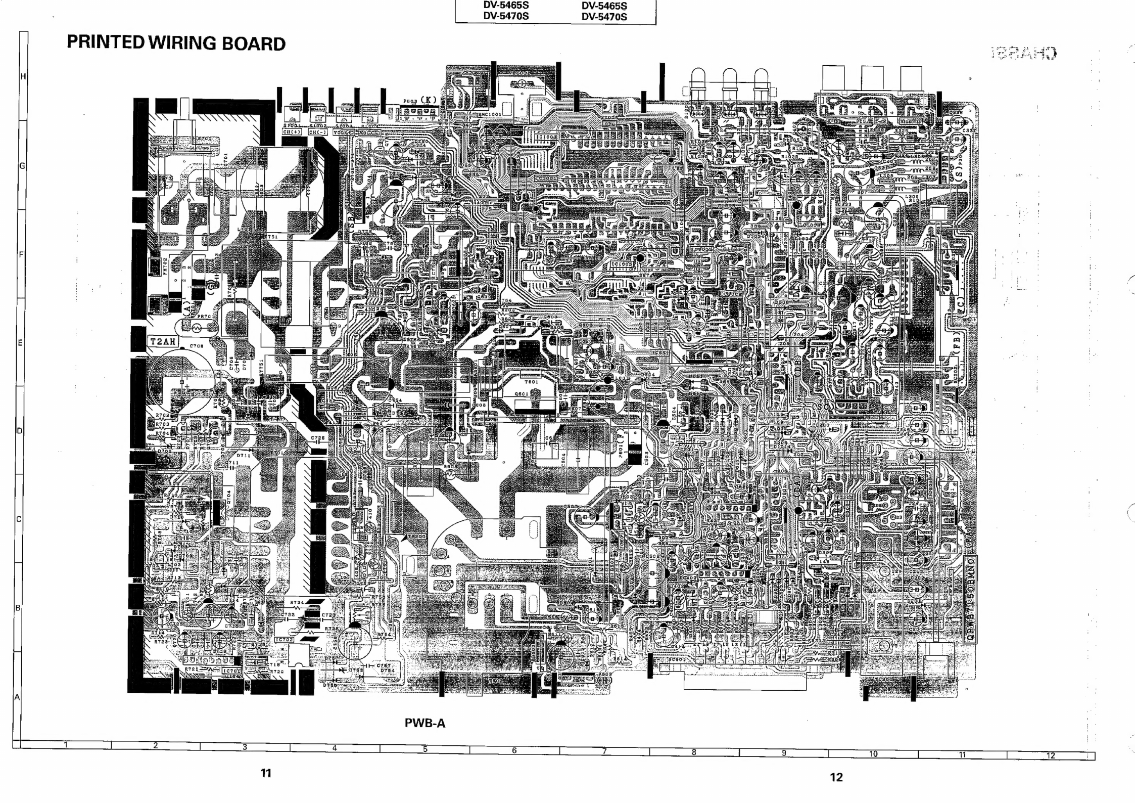
Sharp DV-5465S User manual

UDV-94090
|
DV-5470S
SHARP
_
SERVICE
MANUAL
SEGTDV5465S//
PAL/SECAM
SYSTEM
COLOUR
TELEVISION
4BS-B
Chassis
DV-5465S
mores
DV-5470S_
In
the
interests
of
user-safety
(Required
by
safety
regulations
in
some
countries)
the
set
should
be
restored
to
its
original
condition
and
only
parts
identical
to
those
specified
should
be
used.
CONTENS
e
ELECTRICAL
SPECIFICATIONS
.......:ceseeeeseeees
e«
PRINTED
WIRING
BOARD
ASSEMBLIES
¢
IMPORTANT
SERVICE
NOTES
........cceseeeereees
e¢
SCHEMATIC
DIAGRAM
AND
©
SERVICE
ADJUSTMENT
.......:sssccssssssessscessaaees
WAVEFORMS
eassen
VOU
UORCEOOCOCCOSSCOSST
TCE
Ee
Ce
¢
SOLID STATE
DEVICE
BASE
DIAGRAM
........
*
BLOCK
DIAGRAM
#
CHASSIS
LAYOUT
«ccscssssevccsecssnssssenenissvesesorenss
e
REPLACEMENT
PARTS
LIST
POUR
Ewha
eee
RHR
ERA
e
ED
SHARP
CORPORATION
_

UV-394090
DV-5470S
ELECTRICAL
SPECIFICATIONS
Power
INPUt
.........ceceesessssneanes
220—240
V
AC
50
Hz
Intermediate
Frequencies
Power
COMSUMPTiON
.........ceesesersssssessseresereaes
60
Wh
e
Picture
IF
Frequency
.........cesesessssesessens
38.9
MHz
e
Sound
IF
Carrier
Frequency
.....
33.16/33.4
MHz
Audio
Power
Output
Rating
.............
4W
{MPO}
x2
e
Colour
Sub-Carrier
Frequency
.........
34.47
MHz
SPEAKS
ys
oececeeusceceasitsinaavrawecaceen
10
cm
Round
x2
pes
(Nominal)
Voice
Coil
Impedance
............06.
8
ohms
at
600
Hz
Aerial
Input
Impedance
CONVEFGeNCe
.......cserersene
Self
Converging
System
MIME
ceccsecteactseceoncdceteees
75
ohm
Unbalanced
FOCUS
<i
is\ssnasssaciauleoninnttecs
Bi-Potential
Electrostatic
Tuning
Ranges
..........
48.25
MHz
thru
855.25
MHz
Sweep
Deflection
...........ccecsscecsecseesssseee
Magnetic
CATV
Special
Channels
Specifications
are
subject
to
change
without
prior
notice.
WARNING
The
chassis
in
this
receiver
is
partially
hot.
Use
an
isolation
transformer
between
the
line
cord
plug
and
power
receptacle,
when
servicing
this
chassis.
To
prevent
electric
shock,
do
not
remove
cover.
No
user
—
serviceable
parts
inside.
Refer
servicing
to
qualified
service
personnel.

VV-o40900
|
DV-5470S
IMPORTANT
SERVICE
NOTES
Maintenance
and
repair
of
this
receiver
should
be
done
by
qualified
service
personnel
only.
SERVICING
OF
HIGH
VOLTAGE
SYSTEM
AND
PICTURE
TUBE
When
servicing
the
high
voltage
system,
remove
static
charge
from
it
by
connecting
a
10
k
ohm
Resistor
in
series
with
an
insulated
wire
(such
as
a
test
probe)
between
picture
tube
ground
tag
and
high
voltage
lead.
(AC
line
cord
should
be
disconnected
from
AC
outlet.)
1.
Picture
tube
in
this
receiver
employs
integral
implosion
protection.
2.
Replace
with
tube
of
the
same
type
number
for
continued
safety.
3.
Do
not
lift
picture
tube
by
the
neck.
4
.
Handle
the
picture
tube
only
when
wearing
shatterproof
goggles
and
after
discharging
the
high
voltage
completely.
X-RAY
This
receiver
is
designed
so
that
any
X-Ray
radiation
is
kept
to
an
absolute
minimum.
Since
certain
malfunctions
or
servicing
may
produce
potentially
hazardous
radiation
with
prolonged
exposure
at
close
range,
the
following
precautions
should
be
observed:
1.
When
repairing
the
circuit,
be
sure
not
to
increase
the
high
voltage
to
more
than
30.0
kV,
(at
beam
0
1A)
for
the
set.
2.
To
keep
the
set
in
a
normal
operation,
be
sure
to
make
it
function
on
25.5
kV
+
1.5
kV
{at
beam
1100
A)
in
the
case
of
the
set.
The
set
has
been
factory
—
Adjusted
to
the
above-
mentioned
high
voltage.
-.
If
there
is
a
possibility
that
the
high
voltage
fluctuates
as
a
result
of
the
repairs,
never
forget
to
check
for
such
high
voltage
after
the
work.
3.
Do
not
substitute
a
picture
tube
with
unauthorized
types
and/or
brands
which
may
cause
excess
X-ray
radiation.
BEFORE
RETURNING
THE
RECEIVER
Before
returning
the
receiver
to
the
user,
perform
the
following
safety
checks.
1.
Inspect
all
lead
dress
to
make
certain
that
leads
are
not
pinched
or
that
hardware
is
not
lodged
between
the
chassis
and
other
metal
parts
in
the
receiver.
2.
Inspect
all
protective
devices
such
as
non-metallic
control
knobs,
insulating
fchpapers:
cabinet
backs,
adjustment
and
compartment
covers
or
shields,
isolation
resistor-capacity
networks,
mechanical
insulators
etc.

UDV-34090
DV-5470S
SERVICE
ADJUSTMENT
M@
PIF/SIF/AGC/G2
Adjustment
1.
Trap
Adjustment
Adjusting
Point
O]
11201:
Trap
coil:
(Adj.-P
Trap)
|
1.
Connect
sweep
generator
output
to
IF
in
(FA
(1)).
2.
Connect
response
cable
with
detector
to
collector
line
of
Q1200
(see
diagram).
To
Oscilloscope
GND
3.
Adjust
11201
(Adj.-P
Trap)
so
that
trap
is
(32.4
MHz).
{32.4
MHz)
Trap.
Adj.
P
T1201
2.
VCO
Adjustment
Adjusting
Point
OO
114202:
VCO
adjust
coil
ho
(FA)
in IF
unit.
e
Frequency:
38.9
MHz
(CW)
+
5
kHz
e
Level:
approx.
85
dB
3.
Adjust
T1202
so
that
voltage
at
pin
(7)
(AFT.
output)
of
connector
(FA)
in
IF
unit
is
2.5
+0.2V.
To
Coffector
of
.
7:
Qi200.
.
Apply
DC
2.5V
to
pin
(25)
of
1C1200
(PIF-AGC).
.
Feed
the
following
signal
to
pin
(1)
of
connector
3.
Separation
Adjustment
Adjusting
Point
C1
R1219:
Separation
control
1.
Receive
the
following
signal
from
IGR
stereo
signal
generator.
¢
Video
Signal:
Colour
bar
(875%
mod.)
e
Stereo
Mode:
L
(unmodulated}
‘R
(400
Hz
modulated):
=
Wake
sure
the
unit
is
in
the
stereo
mode
with
OSD
(On-Screen
Display)
on.
2,
Terminate
pin
(3)
(audio
L
output)
of
21-pin
connector
with
10
kQ
impedance.
Adjust
separation
control
(R1219)
until
400
Hz
output
waveform
becomes
minimum.
4.
RF
AGC
Adjustment
Adjusting
Point
{]
R1216:
RF
AGC
contro!
1.
Receive
“COLOUR
BAR”
signal.
*
signal
strength:
53
dB
(terminated
with
75Q)
2.
Connect
DC
voltmeter
to
Test
Point
TP1200
(RF
AGC).
3.
Set
AGC
control
(R1216)
to
maximum
position
(memory).
4.
Adjust
R1216
to
obtain
voltage
of
0.1
V
below
maximum
voltage
(step
3).
_
5,
G2
Adjustment
1.
Receive
“MONOSCOPE
PATTERN”
signal.
2.
Connect
DC
voltmeter
with Test
probe
attenuator
(+
1000)
to
G2
on
PWB-B.
3.
Adjust
Screen
control
to
obtain
700
V
on
G2.
6.
Focus
Adjustment
—
1.
Receive
"MONOSCOPE
PATTERN"
sgnal
2.
Adjust
Focus
control
to
have
best
focus
at
the
central
area
of
CRT
screen.
7.
110
V
Adjustment
1.
Receive
"MONOSCOPE
PATTERN"
signal.
2.
Connect
DC
voltmeter
to
TP700.
3.
Adjust
the
R755
until
the
TP700
voltage
becomes
100V+0.5V.

|
DVv-54708___
M
SERVICE
MODE
FUNCTION
|
This
mode
function
is
provided
to
assist
with
the
settings
of
those
adjustments
that
may
vary
from
one
Picture
Tube
to
another,
or
between
models.
In
order
to
use
the
Service
Mode
ConnectTest
Pattern
signal
to
antenna
terminal.
.
Press
main
switch
to
off.
.
Press
1
V
and
CH
A
buttons
and
main
switch
to
on
simultaneously.
.
—SERVICE
SOFTWARE—
will
appear
on
screen.
RWNo
The
required
adjustments
can
then
be
made
from
the
Remote
Control
Unit.
The
only
buttons
required
are
the
following:
A
CH
V
for
movement
in
adjustment
options
menu;
A
4
V
are
used
to
carry
out
an
adjustment
in
said
menu;
ON/OFF
is
used
to
memorize
a
new
adjustment.
Adjustment
menu
is
as
follows:
—
SERVICE
SOFTWARE
—
CROMA-LUMA
DELAY
—
VERT.
SHIFT
—
HOR.
SHIFT
—
VERT.
BREATHING
—
VERT.
AMPLITUDE
—
§-CORRECTION
—
RED
REFERENCE
—
GREEN
REFERENCE
—
BLUE
REFERENCE
—
ALTER
NVM
POS
00
00
—
ALTER
NVM
VAL
00
00
—
AUTO
INSTALLATION
—
OPC
VALUE
(DV-54705
only)
Having
finalized
adjustments,
to
exit
service
mode,
press
main
switch
to
off.
Adjustment
Note:
The
procedure
for
making
adjustments
to
Vertical
Corrections
is
as
follows:
—
Adjust
S-CORRECTION
—
Adjust
VERT.
SHIFT
—
Adjust
VERT.
AMPLITUDE

DV-5465S
DV:5470S
M@
GEOMETRY
atamiabae
led
PROCEDURE
CHROMA-LUMA
DELAY
a)
Receive
Philips
pattern
signal.
b)
When
volume-up
button
is
pressed,
[uma
phase
delays.
c)
When
volume-down
button
is
pressed,
chroma
phase
delays.
d)
Adjust
the
Chroma-Luma
delay.
.
we
VERT.
SHIFT
a)
Receive
Philips
pattern
signal.
b)
When
volume-down
button
is
pressed,
picture
moves
up.
c)
When
volume-up
button
is
pressed,
picture
moves
down.
d}
Adjust
the
Vertical
location
to
obtain
picture
centering
(fig.
1)...
HOR.
SHIFT
a)
Receive
Philips
pattern
signal.
b)
When
volume-up
button
is
pressed,
picture
moves
to
the
left.
c}
When
volume-down
button
is
pressed,
picture
moves
to
the
right.
d)
Adjust
the
horizontal
location
to
obtain
picture
centering
(fig.
2).
VERT.
AMPLITUDE
a)
Receive
Philips
pattern
signal.
b)
When
volume-up
button
is
pressed,
vertical
size
of
picture
increases.
c)
When
volume-down
button
is
pressed,
vertical
size
of
picture
decreases.
d)
Adjust
the
vertical
size
to
obtain
overscan
(fig.
3).
S-CORRECTION
a)
Receive
Philips
pattern
signal.
b})
When
volume-up
button
is
pressed,
upper
and
lower
scanning
decreases,
and
center
scanning
increases.
c)
When
voiume-down
button
is
pressed,
upper
and
lower
scanning
increases,
and
center
scanning
decreases.
d)
Adjust
the
S-correction
to
obtain
a
balance
between
upper,
lower
and
center
(fig.
4).
Fig.
1
Fig.
2
Fig.
3
Fig.
4

DV-946
The
following
adjustments
are
only
required
when
the
Picture
Tube
is
changed.
RED
REFERENCE
/
GREEN
REFERENCE
/
BLUE
REFERENCE
a)
Adjust
G2.
b)
Tune
in
white
pattern.
c)
Adjust
colour
to
minimum.
d)
Position
colourmeter
in
the
center
of
screen.
e)
Using
brightness
and
contrast
buttons,
select
a
luminance
of
=~
120
NITS.
f)
Operate
again
in
Service
Mode
and
select
location
RED
REFERENCE
/
GREEN
REFERENCE
/
BLUE
REFERENCE
to
obtain
colour
coordinates:
X
=
0.290
+
0.015
Y
=
0.284
+
0.015
g)
Exit
Service
Mode
and
check
colour
coordinates
‘X’
and
“Y’
at
20
and
120-NITS.
It
may
be
necessary
to
repeat
procedure.
NOTE:
Locations:
RED
REFERENCE
alter
‘X’
coordinate;
GREEN
REFERENCE
alter
the
‘Y’
coordinates;
BLUE
REFERENCE
alter
the
‘X’
and
‘Y’
coordinates.
ALTER
NVM
POS
XX XX
Assigned
value
Storage
Location
When
V
-4
A
buttons
are
pressed,
alter
Storage
Location.
ALTER
NVM
VAL
XX
XX
Assigned
value
Storage
Location
When
V
-2
A
buttons
are
pressed,
alter
Assigned
value.
te
be)
DV-5470S

DNE5465S
DW:5470S
SOLID'STATE
DEVICE
BASE
‘CIAGRAM
78"
6
er
aa
a
Pe
pes
lis
ee
2°32)
2
ENTE
Tas
ie
J
a
an
Rgaad:
caren
Salat
tad
ae
cca
ethos
vs
Pup
pees
SVs,
of
"
Seb
AT
Miele
add
cata
Rta
Gs
dee
Ny
AR
eel
oe
Feng
PS
a
ne
Ree
CH-IX1412CUST
CH-IX1456CJTO
RH-IX1473BMZZ
CH-IX1412CJUSU
CH-IX1456CUJT1
-
RH=IX1484;BMZZ.
0:
VHIUPC358C/-1
-
Shana
ot,
e
RAAISSSBNZZ
SOB
HX
goaeMiz2”
RNaxteaemzz
|
BRIE
ya
MN
cee
oy
BMS
|
16
9
RH-FXO101BMZZ
—
VHILA7016//-1
RH-IX1485BMZZ
RH-IX1474BMZZ
VHIKA7805PI-1
VS2SD1554//2E
:
|
|
RH-IX1475BMZz
|
|
20
11
16
9
Oe
et
|
|
eal
co
_
ae
~
1
10
1
3
Sn
1
8
1
3
(SMD
COMPONENT}
(SMD
COMPONENT}
IN
out
|
GND
E
je]
RH-TX0104BMZZ
VHIKIA7045P-1
RH-TX0107BMZZ
RH-TX0119BMZZ
VS2SA1037KQ-1
RH-TX01028M2ZZ
RH-TX0118BMZZ
VS2SC2412KQ-1
RH-TX0106BMZZ
VS25C227-D1A
(SMD
COMPONENT)
Cc
E
ae.
A
oO
m

——
DV-5465S
DV-54655
DV-5470S
DV-5470S
CHASSIS
LAYOUT
851002
§1003
8100)
51004
MAIN
UNIT
DV-5470S
ONLY
VCJI/STEXT
IF/IGR
UNIT
UNIT
i
CFi200
CF1201
CFi202
0
@
R1219
SEPARATION
}
|
x
R1216
CRT—UNIT
9
10

DV-5465S
DV-5465S
DV-5470S
DV-5470S
PRINTED
WIRING
BOARD
se
L|
1
FE
aD
Le
|
ara
tn
aN
=
[icroon
es
ae
MARAE
Se
Nips
Y_righ
See
ay
QPL
ea)
SRIeE=
es
are
ae
a
ial
f
Pap
ope
teenamoeeees)
c
ea
aoc
taaek
Se
SND
Vg
te
Nee
ecient
cet

222M
SO
ao
ati
F
7892BMNS
See
ae
spy
SHARP
ESPARA
bf
FT
a
DV-5470S
DESCRIPTION
OF
SCHEMATIC
DIAGRAM
SAFETY
NOTE:
1.
DISCONNECT
THE
AC
PLUG
FROM
THE
AC
OUTLET
BE-
FORE
REPLACEING
PARTS.
2.
SEMICONDUCTOR
HEAT
SINKS
SHOULD
BE
REGARDEDAS
POTENTIAL
SHOCK
HAZARDS
WHEN
THE
CHASSIS
IS
OPERATING.
IMPORTANT
SAFETY
NOTICE:
PARTS
MARKED
WITH
"A"
(20°
°°
SRN
0)
ARE
IMPORTANT
FOR
MAINTAINING
THE
SAFETY
OF
THE
SET.
BE
SURE
TO
REPLACE
THESE PARTS
WITH
SPECIFIED
ONES
FOR
MAINTAINING
THE
SAFETY
AND
PERFORMANCE
OFTHE
SET.
SERVICE
PRECAUTION:
THE
AREA
ENCLOSED
BY
THIS
LINE
(mm
sam
mmm)
1S
DIRECTLY
CONNECTED
WITH
AC
MAINS
VOLTAGE.
WHEN
SERVICING
THE
AREA,
CONNECT
AN
ISOLATING
TRANSFORMER.
BETWEENTV
RECEIVER
AND
AC
LINETO
ELIMINATE
HAZARD
OF
ELECTRIC
SHOCK.
(1)
6
Vp-p
Q)
520
Vp-p
ff}
)
wor
learen
PERIODE
|
PCreen
rene
NOTE:
1.
The
unit
of
resistance
"ohm"
is
omitted
(K=1000
ohms,
M=Megaohm).
2.
Ali
resistors
are
1/8
watt,
unless
otherwise
noted.
3.
All
capacitors
are
uF
unless
otherwise
noted
4.
The
capacitor
with
Part
No.
RC-FZ9XXXBMNA
is
designed
to
withstand
63V.
WAVEFORM
MEASUREMENT
CONDITIONS:
Colour
bar
generator
signal
of
70
dB
from
RF
input.
CAUTION:
This
circuit
diagram
is
origina!
one,
therefore
there
may
be
a
slight
difference
from
yours.
(4)
1000Vp-p
imal
14

oe
ee
i
oe
DV-5470S
MODEL
DV-5465S
SCHEMATIC
DIAGRAM
Main
Unit
Foo.
go
eh
Es
Ada
col,
BP7Oz
‘Gonoanet
iG}
arc4
a7o3
130K
=
ISOK
=
SOK
Claw
al72w
Li
eeu
AT]
FZ0/
030MN)
Ar20
(30K
1X1424BM
/TEAIOIS
we
:
sipoy
dive
KOOTSOE
00796E
Pee
votes,
Ic751
KATAOSPL
ea
coma
0789
Oxo50ZEM
47
BCS:
H-TXO1GGEM
PTT
10
16M)
1X1
|
G36M
TOABITO
a
ate:
FTSI
FS-4021CE
[wav
>
'
a
_~—_|
1
tier
Ley,
o
QBOT
ss.
7
B40
rae
wsor
it
(")
te
[
Fro
H-=TXO1048M
a
(ayy
J a
KZC(
SCE
Ta
thonee
——}
7
100
o608
AC547
H-TXOtOGBM
H=TXO1046M
s.
7
‘3
Fraz0
10
aby
Mealedadadadadtttyy
taueaenees
{ll
g
4
4
gq
<=
9°
IC
1004
ixiaasemrsn7aars
289928
ud
[3]
[el
1X14128M
aos
88s
8
&
EI
ad
$9asS
e385
g-lOS!
5
@-
IXt4g1BM
il
7
picor
01005
Q)006
Oxneasem
asce4l2 2SC2412
o610
AN
zsczai2
@)
RSI
2
S07
pspz
lew)
joo
1
Bexzoz008M
(35y,
OfGS91BM
AIo16G
<=
cal
Lal
mov
|
saaown
a
FZ647aBMNY
(1G0VE
FZTICABMAL
Creowy
R608
=
pg
18
ceor
$6ee
13K
DXOSi
IBM
TT
Fan
ow
i250v1
FZ63340KND
|}
———
ASi2
a
ace
REiG
22
2
iam
AC
22
cols
*
ye
ReAZOZICA
2
7
aa
32)
72
ow
ZN
1)
FY
AeXZORtCBM
ps
Or
F202240MNd
n
phd
chiA
Agt3
cers
10
3.0
io
snow
PU
how
$14
—'S0¥I
=>
neo?
pad]
oxcossi
bOK
OxnS)20M
i,
IC|OO3
sezcsi2
tit
|
EL
|
Sere
|
CCA
RRR
RReee
Ixl4748M
=
10
2
AESOP
ATS
PV-940900
DV-5470S
(CH-1X1412CUSU)
as
& a
2g
Ar
The
symbo]
——}~-
means
a
resistor
of
1/16
W.
Ic651
KATBO5S2
at
g
i
3
§
=
t
4
64
(SABAOZ2)
Alolz
Algia
2.2K
10K,
22K
RIDIS
“
Riol3
Aiglt
2K
22K
4.7K
22k
BCS47
ae
H+TXO!
O6Bha,
2 2
cac3
4
1164)
IL
Mi
ze
Hi
aS
es
OSIT
DxOOasaM
3
tl/aws
a7
6
Gacz[)
R604
62
470P
Tl
tizawh
ST-BY
/FOW-IN
Bicol
.
PxO2SICE
Alo24
470
ti74wy
asaiosr
(
~
i
pices
«=
RIG
ea
DxOGasem
22K
Riors
mlo7T
Sy
270,
(Kin
io
.
dase
A-xZO2005M
Ic30
|
1k14465M
TDAZOOTA
sca
Le
V
erheshententententemtententententententententenemententeniementendens
a
19K
Ag2e
|
cdi
tare
|
100
=
raze)
Go
eg
HeTXOIO6GM
h2cK
Hy
AIz6
-y
_dlant
Tao"
soll
ain
+
oi.
ial
ear
100
i
Gey
og!
i"
fy
S303
2502412
ie
2
KC)
scoala
fe
ONS
LJce0s
[)c2zoa
(ser
[sar
e306
cxo7
it
47
ay
_tiew
is)
AIOS
mes
=
(ao 190
w7ay
(
fawi
Rios

DV-54655
DV-94095
DV-5470S DV-5470S
MODEL
DV-5470S
SCHEMATIC
DIAGRAM
Main
Unit
The
symbo!
——-—
means
a
resistor
of
1/16
W.
#
L
v___vani
st-by/pow-ty
$ToREO,
PO
tae
ee
—"uaKGoo2
1
ce
E}oa1
ptaol
pioaz
Dios
CF C)
©
2
a
bitdbomcr
Pigenice__—Pgeee
_
Pgedie
BG
Bi
-
cols
=
GH
It
fe)
VOL
Gd
ope
-}
AN
ase
es
eb
ae
wT
RADE
Cc}
+c1o]
15
|
Tio
<6
I
1
|
1
fro
|
{
iAcza0v)
FzZO1a5a
|b
"
QacezziooBUsa
har!
I
<
zioomsa
el
Dn
ia
IX1412BM
(2703)
ove
RIOT?
eior3
|
270
IK
a
fe
eet
da
{
|
aiiGC
{
i
I
t
ure
|
t
j
FOU
OGM
fo
er
ee
ed
(4)
(5)
A
TTS)
AS
podoinm
ana
con.
§P7az
PATO!
Poozece
foacrea
CG)
{
ie]
te
tacenovl
(1
La)
1)
SA
ocros
pray
“7OO#RCE
RYTSU
ol B2
ZB
200018M
tacesov
m9
K2ouzeCE
Algae
ia
100K
:
peas
|
DxooeBou
Sa)
wr!
oe
“’“
O756
22K
BCS47
pnzes
H-TROIOGAM
4.7"
R70q
R703.
RTOZ”
150K
(SOK
[SOK
.
C142W)
C1420
ANEW
ca
O708
et
cieS
Soh
A
ct
A
Vr
yet
sik
ti.
we
SY
Pe
aFaay
H-TXO
1078M
fm
(in
Ie)
ie
wd
eo
asze
|
czar
scpoz
o702
tek
|
toa
Bc54
|7
C4
Wey)
#3,2
|H-TX
|
O1CGBM
inl
a
4)
iss
wa
a
aK
Lt
i
ci
|
eo
su
RTas
eS
Bee
senne
pales
eo
ow
4
PWB-D
34
89
Foo
7H
eye
am
RYI6
A327
100
by
2
By
5
|
el
Ud
fievi
gl!
VCJ
a
nf)
|
OXCOaSEM
71g
{
On-+4
4)
=
Bet
i]
|
—
1"
i
DEIT
BIOs
|
l
|
AT
ccos
cede
Bxooa50M]
DX0G456M
{
lzs0vr}
ita
22K
es
|
I
FZ6474EMAI
1/G0V]
FZTICIEMA
gi
72H)
«too
4
i
4
i)
Faboe
BLN-OOIOCE
i
A
lea
Pad
ZOS33BM
gC557
F2¢104BMeM
TIS
cra
ak
Ixops7ce
06d
ta
ofos
Rol2
OK
oxo
joasaM
pxoo4sam
=
|OK
azop
S307
:
(
SC
a
"SBor
ele
e
tA
ia
a
BC557
i+
ce)
13K
72
neaa
a
Sor,
[ox
J)
H-TXOtO4BM
@
tax
2
—
R63}
hpcd
10K
Ap
teicag
at
g
R4IZ
ZO
C410
IK
RAY
Ls
65
41
/awh
C144aVir
C403
caozpy
R04
at
82
ORF
arr
hea
100K
BI
WeDisece
+a
|-Fca2e
€
7)
mele
Ren
PWB-C
TD
issy:
ex
ee
raw
A)
tives
Ay
ia
330
ez0
IF/IGR
Q608
—
Deis
3
(bea
7
IML
>
R-xzoz
160M
(leva
UAW
OT
aos
RODS
BC54T
EX05236K,
FZa226BMNS
;
a
oy''
sc
H-TXO106BM
t2zvs
R634
a
4.7K
Fooos
@LN-OOFTCE
30
too
1016
UL
1a
DbO3
H-TXOJ045M
3.
—150v1
oxos
rape
{6
IC7Ol
1x1424BM
/TEAIOI9
'3-
gaze
'
c606
es
V2
|
8CS57
Ai
pI}
050s
ok
1c402
cacpat
pat
pet
pak
ak
csc
pk
Per
yal
ae
ee
DXOOS5BM
2
LA7TCIB
,
Sobkocolyocasycayo
co
ecoycoyey
cole
=
Om
—CHIiPEo2
V=OUT
Aen
.
aa
‘
Bt
i=-0uT!
R-OUT
we,
ee
4
20)
1g
16
4
a
1
ee
a
AD
\_¥eIN
BLK
SLOW
L~IH
Rew

DV-54655
DV-5465S
DV-5470S
DV-5470S
:
MODELS
DV-5465S
and
DV-5470S
SCHEMATIC
DIAGRAM
SS
:
ee
Note:
The
symbol
———~
means
a
resistor
of
1/16
W.
Wl
IF/IGR
Unit
Riz10
91201
Al212
a
i
25C1906
5
i
-
22K
(XF)
01303
1
133
1
:
s
2K
:
2sc2412
tov)
;
:
c1iZz19
-
aT
Ol3s3l
a
:
Y
H-TXOt}3BM
6.
.
‘
j
X13)
2
ciLog23s¢
E>)
cei2z02
BOOORM
7
wv)
ao
mae:
a
cane
RlzZe
‘
;
H
Sel
cy
LCI
304
—7———7._s
I
decisze
ee
.
1x14458M
cisz0
f].co1
(ACP237
tD
ad
R
220
Ol
t174W)
AeA
PERE
Ere,
—
vcc
VIF
GND
vP/2
AFT
oo
VIDEO
OSS)
AF
~
(S¥}
AGC
OUT OuT OUF AGC
IN
YSUP
a
T¥IM2
NC
TVIN]
AUX AUX AUX AUX
YVSUP
POUT
ANACOG
ANACOGIN
IN2
INI
GCIN2
DINI
VREF
GNO
CF
1200
4S,SMHz)
co06|CE
Oxco458m
TDAS8I3T
FM/AM
FM
PIF
=IN
CVBS
L/L’
AUDIO
AUDIO
DEC
=~DEC
IN
—"_BLO_TADJ
TPLL
S-accSED
OUTI2VI
OUTI
OUT2
CAPZ
CAP)
FM2
2)PIN
s
a)
|
ouTi
DAC
OUT2
2L
bac
DAC
VA
POMC|
PDMC2PDOMC3
BAI
2R
IREF]
IL
RI203
4.9
B77°5
22K
64m
tAZa]ta
GBAKARK
Itz.
21
Ri2z08
12]
33Q]/]Ri23/5
cl2io
IK
1
4701
P
FU}
r0o
tt
=
I
MF
lz01
abe
COO63CE
81206
C]
cl2i
(5.74MH:z)
:
r
,
te
Lae
!
0
—|
:
7
ry
as
:
a
. : : ;
&
. .
=z
.
:
to
|
150
Fctzo3
loo
7
7
C1354
C1385
C1356
C1357
C1356
im
SF1200
Rl2IT
t16¥)
ae
22
680P
s80P
680P
015
015
ae
=
a
on
-
r}cl201
CO108EM
clzo8
rs
ee
RIZI9
je
|
i
lav
H.00)
al
MU)
4.7K(B)
;
no
|
FZ9104BMNJ
1209
M4077CE
22
as
Li
;
22P
;
:
F29224BMNJ
22
alae
(I-44)
ie
iM
SEPA|
RATION]
150
a
Ai2IG
22Kta)
BIGOTAE
7120)
(3)
CILIO40zce
Ri2zo
©
pL
6.8K
Ld
ChI6?
C366
a
-
6-01
a)
Risis
||
1 |
RI348
we
Be
ioe
|
Tt?
100
Lt)
+clz2t
_
RI35I
aay
a
a
Ce
|
PWB-C
tt
ievi
fivew
a
ae
ee
i
a
DUNTK7
|
48BMVO/v!
tray
?!200
Bo
100
‘
mAs
sem
ke
oe
se
om
hook
ee
-—
wash
ho
Sk
hd
k-th
a =
(Fi
—
CE
el
(i)
GE
(
--2,-2.
9,0
9
9
Ono
OO
SO
OOO
OOF
eC
G)
“@~
“6S
©
eae
IF
GND
12V
AGC
V-
P-DET
AFT
5V..
NC
NC
R L
GND”
R
tL
GND.
OR
tc
oGMD
OL
RESET
GND
SCL.
SDA
IMD
NC
MUTE
OUT
OUT
;,
4
a
7
‘i
ry
21PIN
QUT
co
FRONT
IN
o
ZIPIN
IN
TY
OUT
19
20

V-5465S
DV-54655
DV-5470S
DV-5470S
ae
DV-5465S
and
DV-5470S
SCH
EMATIC
DIAGRAM
Note:
The
symbo!
———}-
means
a
resistor
of
1/16
W.
CRT
Socket
and
VCJ/TEXT
Unit
25.5K¥
Cav)
Stas)
GAT
Sommer
ay
PWB-B
(CRT
UNIT)
120
BeA2
sane
DUNTK7092BMY7
(DV-5470S)
Dit
sou
—
ome)
DUNTK7092BMZ3
(DV-5465S)
Ci
Baconcou
,
BF422
pase
a
reas
craze
|
ss
470P
e;
"
;
cer
|
{Re
oara
mee
TXO1248M
H~TXO
avoP
a:
—s
-
SEs
H-TXOJ10
TO
PWA-A
tf)
C)
OWOKO)
®
|
HO
SS
30h
oe
aGeo
ae
Oo
6
OS
=
—
3
a7
yew
!
i”
C2802
;
IX1495BM
:
MC44
140)
Se
apanai
DIIDI
7
'
1
:
;
4.7K
i
|
C1101
|
:
isDasers)
|
:
IX1573BM
|
(MC44007)
Fee
:
F
tog
|
Pea]
|
aa
:
DD
Dg
LN
Sr
-
f
:
|
pp
yy
N

DV-5465S.
DV-5465S
DV-5470S'
DV-5470S
1
Seene
nnn
anny
’
OV-5470S
ONLY
fee
se
es
ey
ee
Ce
ees
SMe
ae
eee
~
R
u
v
}
I
FRONT-AV
;
FMCIOOI
I.
sl005
f™
7
1
I
ST-BY
STEREG!
opc
GW)
CH
&)
(4)
VOL:
ery
ws
H
POWER
eo
ee
\RMC(CO}
i
LIL
ae
a
|
orc-sw
|
iS
1
|
"RECEIVER:
apa
|
‘
’
|
el
as
Eo
D100!
prone
01003
|
=
MICRO-—PROCESSOR
__
|
beeesaaie
1
EE
CRY
eke
ITC
SPE
Pee
me
Oe
a
KEY-SWICH
Ici003
C1004
I
|
:
EP-ROM
’
SHIFT
RESISTOR
|
ar
1930
:
0755
:
®
O
SOUND-OUT
(S)
ae
|
c
}
|
p-——<femron_|
Sane
;
\
.
IC1001
ae
hale
|
MICHO-PROCESSOR
)
2@
Toeecens
a
Ic65i
eee
a
|
o
29)
can
an
on
1
C
|
i
(Ai
on
La
be
a301
o502
{
9
S;
73)
0303
DI04
cS)
ADG
COIL|ig)
Prva
IC1007
-
oe
ee
ae
:
|
ee
=
ig
|
me
POWER
ON/OFF
|
Gal
>
@4—
7)
070
|-D704
|
‘
a
Ne
oe
t
[ciag5
i
AFT
PWE-cC
-
JOUNTKT
1
48BMY
|
/¥O
IF/IGR
UNIT
VCJU/TEXT
UNIT
IcsO|
VERTICAL~OUT
Pwa-0
DUNTK?
|
49BMVO
;
(0c)
Iviceo-MuTe
|
3]
[soa
fal
Toren
tas
OS
ea
n
a
=
1)
Xa)
Nolatar
©
ya
i
a
io
7
Y
{|
4
2
[=]
{|
»
fn]
a}
meee
Xo
Ca)
Cake
i
OUT
4d
Hl
ia
(eXoX=X
VIRTICAL-IN
Or
VIRTICAL-SIZE
Ps)
X10)
Nc
on
.
Bool
|
Ee
Sample
so
g
o
rs]
IN
[A
|
7]
poe
3
ee
Cees)
ia
El)
oe
re
Be
aaa
|
|
9
=
.
COME!
ze!
KU)
Li
[uy
2]
<
ea
i
2X
(FA)
|
sv
a]
acy
*
geor
|
AFT-GUT
iy
H-OUT
casa
PICTURE-ouT
|
6
|
25
:
VIDEO-MUTE
om
pe
3]
pp
=r
Teo!
Ss
¥
:
Po""A
|
onoz
ocos
|
3
or
[so
tet
!
oe
:
Ic2802
|
&
a
sae
Gg
Cea
El
<J
Ace
J
ey
9
VIRTICAL-OUT
|
8
|
ae
1
Of
oo
TF
G)
d
7G
7)
6}
1c702
ba
~
8
7
nd
©
H
[ao
wales
;
-
vinriont
5
Lor200]
4
Oras
TT
il
=[»[«[=[ofo|
as
=,
R755
R724
725
.
c
i(0V-anu
T6o02
mec
PROTECTOR
2
A
DUNTK7
|
SOBMY
2/¥I
0606
9607
g
MAIN-UNIT
Bi
hat
e777
——
iat:
etalk
ie
iter
|
mie
oad
.
.
C2
5
a
ds
i
ee
|
naa
TUNER
=
\yrour
R=IN
sy
Foy
LooufT
R-_
{S690}
Tuzo}
‘
18 16 14
ey
i
oo
Z|
ou
Nes
ee
ee
Stow
t=IN
rN
J
EURO-SCART

Wi
Tuner
NOTE:
The
parts
here
shown
are
supplied
as
an
assembly
but
not
independently.
a
or
fz
P74
cip
ro
Mi
oy,
SRL
fre
ue
Ee
Se
i
n'Q
ie
i
Tet
ETE
pI
4
cy
is]
=a
WEOr
SURIe
QA
hi
1ZOP
te
a4
7%
Od
ut
coe
niche
oe
oa
”
eu
or
ur
Ld
ia
<x
i
ishle4+e
bm
(ee
Rall
wruzezA.
1per
as
Tr
oT
=
z
iM
ce
tar
Tea
T”
bid
Hi
Remote
Control
Unit
NOTE:
The
parts
here
shown
are
supplied
as
an
assembly
but
not
independently.
(ci
MSD467-|34FP
(RH-IX1
469BMZZ)}
Jes!
ee
VV"I4000
DV-5470S
or
vote
cz
TI
e723)
OAR
cue
3.
Hvzare
g70e,
1n3tne
an
es
IR
om
330
M+
t
we
—*
iat
o3
Lat
yor
Ria
za
Azo
HMUI00a
S39
\eagea
$2.18
iM
can
4
Lit)
tie
BSI
a7
?
ta
,
1
a
ad
a
a
i
(3
‘TE?
CORO
mEO:
R208
|
SPSS10
*TSASSIL
[3
41
woeob
ew
YW
RRMCG1023BMSA
KW
STORE
RED
EtyS=SET
y
NW,
VCR
ve
te
CYAN
cy
YELLOW
REVEAL
7,
GREEN
cA
ay,
Si,

DV-5465S
~-
DV-5470S
PARTS
REPLACEMENT
Replacement
parts
which
have
these
special!
safety
characteristics
identified
in
this
manual:
electrical
components
having
such
features
are
identified
by
“A\”
in
the
Replacement
Parts
Lists.
The
use
of
a
substitute
replacement
part
which
does
not
have
the
same
safety
characteristics
as
the
factory
recommended
replacement
parts
shown
in
this
service
manual
may
create
shock,
fire
or
other
hazards.
“HOW
TO
ORDER
REPLACEMENT
PARTS”
To
have
your
order
filled
promptly
and
correctly,
please
furnish
the
following
informations.
1.
MODEL
NUMBER
2.
REF
NO,
3.
PART
NO.
4.
DESCRIPTION
5.
CODE
6.
QUANTITY
MARK
*
:
SPARE
PARTS-DELIVERY
SECTION
Part
No.
Ref.
No.
Description
Code
PICTURE
TUBE
A
V1
VBS1EAL3011°N
S$
CRT
51cm
{21")
CL
RCiLGO408BMZZ
S$
Degaussing
{ADG)
Coil
AP
—
End
of
PICTURETUBE
——.
PRINTED
WIRING
BOARD
ASSEMBLIES
{
NOT
REPLACEMENT
ITEM
)
PWB-A
DUNTK7150CJV2
-
Main
Unit
=
(DV-5465S)
PWB-A
DUNTK7150CJV1_—
Main
Unit
=
(DV-5470S)
PWB-B
DUNTK7092BMZ3
—
CRT
Socket
Unit
=
.
(DV-5465S}
PWB-B
DUNTK7092BMY7
—
CRT
Socket
Unit
a
(DV-5470S}
PWB-C
DUNTK7148CJV1_—_IF/IGR
Unit
=
|
(DV-5465S)
PWB-C
DUNTK7148CJVO
—
IF/IGR
Unit
=
(DV-5470S)
PWB-D
DUNTK7149BMVO
—
VCJ/TEXT
Unit
=
——
End
of
PW.B.ASS’Y
——
_
ERSATZTEILLISTE
{AL
cl
j
AUSTAUSCH
VON
TEILEN
Ersaizteilte,
die
besondere
Sicherheitseigenschften
haben,
sind
in
dieser
Anleitung
markiert.
Elektrische
Komponenten
mit
solchen
Eigenshaften
sind
in
den
Ersatzteil
durch
“AA”
gekenn-zeichnet.
Der
Gebrauch
von
Ersatzteilen,
die
nicht
deselben
Sicherheits-
eigenschaften
haben
wie
die
vom
Hersteller
empfohlenen
ud
in
der
Bedienungsanleitung
angegebenen,
kdénnen
zur
Ursache
von
Blitzeinschlagen,
Branden
und
anderen
Gefahren
werden.
“WIE
MAN
ERSATSTEILE
BESTELLT”
Damit
Ihre
Bestellung
promt
und
korrekt
ausgefiihrt
wird,
geben
Sie
bitte
folgende
Informationen.
.
1.
MODELL
NR.
2,
REF
NR.
3.
ERSATZTEIL
NR.
4,
BESCHREIBUNG
5.
KODE
6.
QUANTITAT
MARKIERUNG
*:
ERSATZTEILE-LIEFERUNG
Ref.
No.
Part
No.
*
Description
Code
PWB-A
DUNTK7150CJV2/v1
MAIN
UNIT
TUNER
|
NOTE:
THE
PARTS
HERE
SHOWN
ARE
SUPPLIED
AS
AN
ASSEMBLY
BUT
NOT
INDEPENDENTLY.
=
A
TU201
VTUATEKES9-052
S$
Tuner,
VHF/UHF
BK
INTEGRATED
CIRCUITS
IC20t
RH-iX0037CEZZ
R
Zener
IC
AF
IC301
RH-iX1446BMZZ
S
Sound
Output
AK
C401
VHiILA7016//-1
R
Video
Switch
AH
[C402
VHiLA7016//-1
R
Video
Switch
AH
{(DV-5470S)
:
IC501.
=RH-iX1163BMZZ
~—s§
_
Verticai
Output
AM
IC651
VHIKA7805Pi-1
R
5V
Regulator
AE
A
1C701
RH-iX1424BMZZ
=e
S-:-«iX1424BM
AN
A,
1€702
=
RH-FX0101BMZZ_
=
§_Photo
Coupler
AE
IC751
VHiKA7805Pi-1
R
KA7805Pi
AE
IC1001
RH-iX1481BMZZ
S
Microprocessor
AS
IC1002
CH-iX1456CJT1
S
EEP-ROM
(DV-5465S}
AP
IC1002
CH-iX1456CJTO
S
EEP-ROM
(DV-5470S)
AP
1C1003
CH-iX1412CJSU
S
EP-ROM
(DV-5465S)
AU
1€1003
CH-iX1412CJST
S
EP-ROM
(DV-54708)
_
AU
{C1004
RH-iX1485BMZZ
=
§
Shift
Resistor
AK
1C1005
VHIUPC358C/-1
R
AFT
AD
IC1006
RH-iX1474BMZZ_—S._
Input
AE
IC1007
RH-iX1475BMZZ
S$
Output
AE
C1008
VHIUPC358C/-1
R
UPC358
*
AD
{(DV-5470S)
IC1009
VHiIKiIA7045P-1
R
KiA7045P
AD
26

es
Ref.
No.
Part
No.
*
Description
Code
PWB-A
DUNTK7150CJV2/V1
MAIN
UNIT
(Continued)
TRANSISTORS
Q200
VS2SC2412KO-1
R
28C2412
AA
0301
RH-TX0104BMzZzZ_
$
BCS5S57
AA
0302
RH-TX0106BMZZ
S$
BC547
AB
Q303
VS2SC2412KO-1
R
28C2412
AA
0304
VS2SC2412KO-1
R
28C2412
AA
Q401
RH-TX0106BMZZ_
S$
8C547
AB
0403
RH-TX0106BMZZ
S$
BC547
AB
0404
RH-TX0106BMZZ
S$
BC547
AB
Q405
VS2SC2412KO-1
R
28C2412
AA
Q501
RH-TX0102BMZZ_
S
BC338
AB
A
Q601
VS2SD1554/2E
R
2SD1554
AL
0602
VS2SC2271-D1A
——-R_
28C2271
(D)
AD
Q603
RH-TXO106BMZZ_
S
BC547
AB
\
Q606
RH-TX0104BMZZ
S
BC5S57
AA
:
0607
RH-TX0104BMzZ_
S$
BC557
AA
Q608
RH-TX0106BMZZ
S$
BC547
AB
Q609
RH-TX0104BMZZ_
S_BC557
AA
Q610
VS2SC2412KO-1
R
2SC2412
AA
A.
0701
RH-TX0107BMZZ_
$_
BF487
AC
A.
0702
RH-TX0106BMZZ_
$
BC547
AB
A
0703.
-RH-TXO118BMZZ
S$
_BC635
AC
A.
0704
RH-TXOM9BMZZ
$
MJF18006
AL
Q755
RH-TX0102BMZZ
S$
BC338
AB
Q756
RH-TX0106BMZZ
S$
BC547
AB
Q1001
VS2SA1037KO-1
_R
2SA1037
AA
01002
VS2SC2412KO-1
R
28C2412
AA
Q1003
VS2SC2412KQ-1
R
28C2412
AA
(DV-5470S)
Q1004
VS2SC2412KO-1
R
28C2412
AA
01005
VS2SC2412KQ-1
R
28C2412
AA
Q10068
VS2SC2412KQ-1
R
28C2412
AA
01007
VS2SC2412KO-1
R
28C2412
AA
Q1008
VS2SC2412KO-1
R
28C2412
AA
01009
VS2SC2412KO-1_R
2S8C2412
AA
Q1010
VS2SC2412KO-1
R
2$C2412
AA
|
Q1011
VS2SA1037KO-1
RR
2SA1037
AA
01012
VS28C2412KO-1
_R
28C2412
AA
01014
VS2SC2412KO-1
_R
28C2412
AA
Q1015
VS2SA1037KQ-1
RR
2SA1037
AA
|
01017
VS2SC2412KQ-1
_R
28C2412
AA
!
|
DIODES
D200
RH-DX0045BMZZ
A
1N4148
AA
D501
RH-DX0501BMzZzZ
S$
1N4004
AA
D502
RH-DX0501BMZZ
§
1N4004
AA
D503.
RH-EX0437BMZ2Z
SS
Zener
Diode,
12V:
AC
D504
RH-DX0045BMzzZ
S$
iN4148_
~
AA
|
D505
RH-DX0045BMZZ
S
1N4148
AA
|
D506
RH-DX0045BMZz
S$
1N4148
AA
|
D602
RH-DXO511BMZZ
-S
1N4935—
AB
D603
-RH-DX0512BMZZ
S
1N4936
AB
Ref.
No.
PPPPBPBPPRPPRPPBRBPRPRPRE
27
D604
D607
D608
D609
D610
D611
D612
D613
D614
D615
D616
D617
D618
D701
D702
D703
D704
D705
D706
D707
D708
D709
D710
D711
D712
D713
D714
D715
D751
D752
D753
D754
D760
D761
D762
D763
D764
D765
D766
D770
D771
D775
D1001
D1002
D1003
D1004
D1005
D1006
D1007
D1008
01003
D1010
|
__Dv-5470S
Part
No.
*
Description
DIODES
(Continued)
RH-DX0512BMZZ
S
1N4936
RH-DX0045BMZZ
1N4148
RH-DX0045BMZZ
1N4148
RH-DX0045BMZZ
1N4148
RH-DX0045BMZZ.
41N4148
RH-DX0045BM2ZZ
1N4148
RH-EX0408BMZZ
RH-EX0423BM2ZZ
RH-DX0045BMZZ
VHDDAN202K/-1
VHDDAN202K/-1
RH-DX0045BMZZ
RH-DX0511BM2ZZ
RH-DX0502BMZZ
RH-DX0502BM2ZZ
RH-DX0502BM2ZZ
RH-DX0502BMZZ
RH-EX0419BMZZ
RH-DX0045BMZZ
RH-DX0045BM2ZZ
RH-DX0509BMZZ
RH-DX0045BMZZ
RH-DX0509BMZZ
RH-DX0515BM2ZZ
RH-DX0045BMZZ
RH-DX0510BMZZ
RH-DX0510BM2ZZ
RH-DX0510BMZZ
RH-DX0246CEZZ
RH-DX0512BMZZ
RH-EX0410BMZZ
RH-DX0514BMZZ
RH-DX0045BMZZ
RH-EX0412BM2ZZ
RH-DX0502BMZZ
RH-DX0502BM2ZZ
RH-DX0502BMZZ
RH-DX0502BMZZ
RH-DX0045BM2ZZ
RH-DX0045BM2Z2
RH-DX0045BMZZ
RH-DX0514BMZZ
RH-PX0291CEZZ
RH-PX0291CEZZ
RH-PX0291CEZZ
RH-DX0045BMZZ
|
RH-DX0045BMZZ
RH-DX0045BMZZ
RH-DX0045BMZZ
RH-DX0045BMZZ
VHDDAN202K/-1
VHDDAN202K/-1
S
$
S
S
S
S
S
S
R
R
S
S
S
Ss
S
S
S
S
S
S
S
S
$
S
S
S
S
R
S
S
S
S
S
S
S
S
Ss
S
S
S
S
R
R
R
S
S
S
S
S
R
Zener
Diode,
5.1V
Zener
Diode,
22V
1N4148
DAN202K
DAN202K
1N4148
1N4935
1N4005
1N4005
1N4005
{N4005
Zener
Diode,
15V
1N4148
1N4148
DX0509BM
1N4148
DX0509BM
1N4148
DX0510BM
DX0510BM
DX0510BM
1N4936
Zener
Diode
MR852
1N4148
Zener
Diode,
75V
1N4005
1N4005
1N4005
1IN4005
1N4148
1N4148
1N4148
MR852
ST-BY/POW-IN
STEREO
OPC
(DV-5470S)
1N4148
1N4148
1N4148
1N4148
IN4148
~DAN202K
-
7
(DV-5470S)
>
DAN202K
(DV-54708}_
Code
AB
AA
AA
AA
AA
AB
AB
AA
AB
AB
AA
AB
AA
AA
AA
AB
AA
AA
AB
AA
AB
AB
AA
AB
AB
AB
AD
AB
AB
AC
AA
AB
AA
AA
AA
AA
AA
AC
AC
AC
AC
AA
AA
|
AA
AA
AB
AB

DV547
IS
Ref.
No.
~
Part
No.
*
Deseiption
-
Code
PWB-A
DUNTK7150CJV2/v1
MAIN
UNIT
(Continued)
DIODES
(Continued)
:
D1011
VHDDAN262K/-1
R
DAN202K
AB
“D1012.
VHDDAN202K/-1
R
DAN202K
AB
D1013.
RH-DX0045BMZZ
S
1N4148
AA
D1014
RH-DX0045BMZZ
S
1N4148
AA
D1015
RH-DX0045BMZZ
S
1N4148
AA
°D1016
VHDDAN202K/-1
R
DAN202K
'
AB
DB1021
VHDDAN202K/-1
R
DAN202K
AB
D1022
VHDDAN202K/-1
R
DAN202K
AB
D1023
RH-EX0409BMZZ
S
Zener
Diode,
5.6V
~
AA
D1024
RH-DX0045BM2ZZ
S
1N4148
AA
D1025
RH-DX0045BMZZ
S
1N4148_
AA
PACKAGED
CIRCUITS
4v
PR701
RMPTPOO28CEZZ
R
Positive
Coefficient
AG
Thermistor
X1001
RCRSBO2Z09BMZZ
S§S
Crystal
AG
COILS
AND
TRANSFORMERS
L601
RCiLZO707BMZZ
~
=
§S
Coil
AH
AX
L701
RCiLFO110BMZZ
S
Line
Filter
AL
A,
1703
~=VP-CF120K0000
R
Coil,
12H
‘AB
1704
VP-CF3R3K0000
R
Coil,
3.3H
AB
L705
VP-CF3R3K06000
R
Coil,
3.3uH
AB
L751
RCiLPO213BM2ZZ
Ss
SS
Coil
AF
T601
RTRNZOO26PEZZ
~=R
Trans.
AH
A,
T6002)
RTRNF2026BMZZ_
S
FlybackTrans.
(FBT)
BD
A
7701
RTRNZOS33BMZZ_
S
Trans.
AV
4
1751
RTRNPOOO1BMZZ
S
PowerTrans.
AS
CONTROL
R755
RVR-M4156GEZZ
R
300
(B)
AB
CAPACITORS
C201
VCEAGAITHW105M
R
1
50V
Electrolytic
AC
C202
VCEAGAICW106M
R
10
16V
Electrolytic
AA
C203.
VCKYTV1HF103Z
RK
0.01
5OV
Ceramic
—
AA
C204
VCKYTV1IHFI03Z
FR
0.01
50V
Ceramic
‘AA
C205
VCEAGAICW106M
R
10
16V
=
Electrolytic
AA
C206
VCKYPATHF103Z
Rf
0.01
50V
Ceramic
AA
C207.
VCEAGAIHW106M
R
10
50V
Electrolytic
AC
C208
VCCCTVIHHS60J
R
5ép
50V
Ceramic
AA
C209
VCCCTVIHHS560J
RF
56p
50V
Ceramic
AA
C210
VCEAGATCW106M
R
10
16V—
Electrolytic
AA
'
C211
VCKYTV1HF103Z
R
0.01
5OV
Céramic
‘AA
C214
VCCCTVIHH470J
R
47p
50V
Ceramic
AA
C306
VCEAGAICW476M
R
47
16V
Electrolytic
AB
‘C307
VCEAGA1CW476M
R
47
16V_
Electrolytic
AB
C309
VCCCTVIHHS560J
R
56p
50V
Ceramic
AA
28
Ref.
No.
Part
No.
*
Description
Code
CAPACITORS
(Continued)
C310
VCCCTVIHH560J
R
56p
SOV
Ceramic
AA
C311
VCCCTV1HH560J
R
56p
50V
Ceramic
AA
C312.
VCCCTVIHH560J
R
56p
50V.
Ceramic
AA
C315
VCEAGAICW107M
R
100
16V
Electrolytic
AB
C316
VCEAGAICW107M
R
100
16V
Electrolytic
AB
C317.
VCEAGAIHW475M
R
4.7
50V
Electrolytic
AB
C318
VCEAGATHW226M
R
22
50V
Electrolytic
AB
C319
VCEAGA1CW227M
R
220 16V
Electrolytic
AC
C320
VCEAGAICW227M
R
220
16V
Electrolytic
AC
C321
VCEAGA1CW108M
R
1000
16V
Electrolytic
AD
C322
VCEAGAICW108M
R
1000
16V_
Electrolytic
AD
‘C323.
~VCEAGAIEW477M
R
470
25V
Electrolytic
AD
324
VCEAGA1HW475M
R
4.7
50V
Electrolytic
AB
C325
VCKYTV1HB102K
R
1000p
50V
Ceramic
AA
(DV-5470S)
C326
VCKYTVIHB102K
R
1000p
50¥V
Ceramic
AA
“
,
(DV-5470S)
C332
VCKYPA2HB102K
R
1000p
500V
Ceramic
AA
‘i€333.
RC-FZ9104BMNJ
S
0.1
50V.
Mylar
AB
C334
RC-FZ9104BMNJ
S
0.1
50V
Mylar
AB
C337
VCEAGAICW107M
R
100
16V
Electrolytic
AB
-(DV-5470S)
C338
VCEAGAICW107M
R
100
16V
Electrolytic
AB
.
(DV-5470S}
C339
VCEAGAICW476M
R
47
16V
Electrolytic
AB
C340
VCEAGAiCW107M
R
100
16V
Electrolytic
AB
C341
VCEAGA1CW107M
R
100
16V_
Electrolytic
AB
C344
VCEAGA1CW107M
R
100
16V
Electrolytic
AB
C345
VCEAGAICW107M
R
100
16V
Electrolytic
AB
C346
VCKYTV1HB102K
R
1000p
50V_
Ceramic
AA
C347
VCKYTV1HB102K
R
1000p
50V
Ceramic
AA
C401
VCEAGA1CW476M
R
47
16V
Electrolytic
AB
C402
VCCCTV1IHH471J
R
470p
50V
Ceramic
AA
C403.
VCEAGAICW476M
R
47
16V
Electrolytic
AB
C404
VCEAGAICW476M
R
47
16V
Electrolytic
AB
°C405
VCEAGA1ICW107M
R
100
16V
Electrolytic
AB
C406
VCKYTV1HF103Z
R
0.01
50V
Ceramic
AA
C407.
VCEAGAICW476M
R
47
16V
Electrolytic
AB
(DV-5470S)
C410
VCEAGA1CW337M
R
330
16V
Electrolytic
AC
(DV-5470S)
C411
VCEAGAICW476M
R
47
16V
Electrolytic
AB
C412
VCEAGAICW107M
R
100
16V_
Electrolytic
AB
C416
VCKYTV1HB103K-
R
0.01
50V
Ceramic
AA
C417.
VCCCTV1HH471J
R
470p
50V_
Ceramic
AA
(DV-5470S)
C501
VCKYPA2HB102K
R
1000p
500V
Ceramic
AA
C503.
VCEAGAIEW108M
R
1000.
25V
Electrolytic
AD
C505
VCEAGA1VW477M
R
470
35V—s
Electrolytic
AD
C506
RC-FZ9333BMNJ
S
0.033
63V
Mylar
AB
‘C507
+
VCEAGAIVW107M
R
100
35V
Electrolytic
AC
C508
RC-FZ9684BMNJ
S
0.68
63V
Mylar
AD
C509
VCEAGAICW107M
R
100
16V
Electrolytic
AB
C511
-RC-FZ9105BMNJ
=
§:
1
63V.
Mylar
AD
C512)
=
VCCSTV1HL471J
R
470p
50V
Ceramic
AA
This manual suits for next models
1
Table of contents
Other Sharp TV manuals

Sharp
Sharp 20F550 User manual

Sharp
Sharp 21HS-50H User manual

Sharp
Sharp 20MR10M User manual

Sharp
Sharp 27C540 User manual

Sharp
Sharp CL32S40 User manual

Sharp
Sharp 27K-S100 User manual

Sharp
Sharp 51AT15H Service manual

Sharp
Sharp LC-48CFE4042E User manual

Sharp
Sharp 26SL72M User manual

Sharp
Sharp LC-20S5X User manual

Sharp
Sharp 81GF-66E User manual

Sharp
Sharp 14LK22 User manual

Sharp
Sharp 19R-M100 User manual

Sharp
Sharp LC-40FI5122E User manual

Sharp
Sharp 20N-S100S User manual

Sharp
Sharp Aquos LC-32LD171K User manual

Sharp
Sharp 21S-FX10F User manual

Sharp
Sharp Aquos LC-52SE94U User manual

Sharp
Sharp Aquos LC-65SE94U User manual

Sharp
Sharp SV-2588H(BK) User manual