Shenzhen JiXinInteligence XR-50B User manual

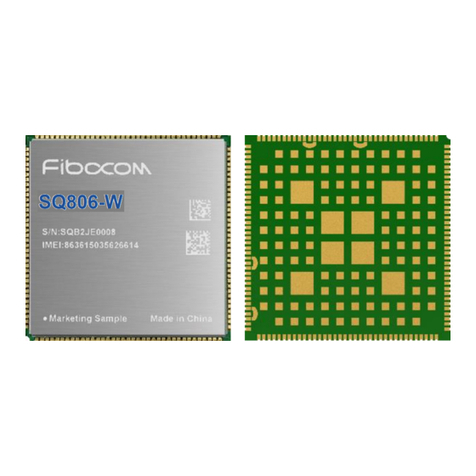
XR-50B WIFI module
Copyright © 2019 ShenzhenJiXinInteligence Co., Ltd All Rights Reserved
XR-50B User manual
Version V1
Copyright ©2019

XR-50B WIFI module
Copyright © 2019 ShenzhenJiXinInteligence Co., Ltd All Rights Reserved
Page 1 of 17
This device is intended only for OEM integrators under the following conditions:
1) The antenna must be installed such that 20 cm is maintained between the antenna and users, and
2) This device and its antenna(s) must not be co‐located with any other transmitters except in
accordance with FCC multi‐transmitter product procedures. Referring to the multi‐transmitter
policy, multiple‐transmitter(s) and module(s) can be operated simultaneously without C2P.
3) For all products market in US, OEM has to limit the operation channels in CH1 to CH11 for 2.4G
band by supplied firmware programming tool. OEM shall not supply any tool or info to the end‐user
regarding to Regulatory Domain change.
USERS MANUAL OF THE END PRODUCT:
In the users manual of the end product, the end user has to be informed to keep at least 20cm
separation with the antenna while this end product is installed and operated. The end user has to be
informed that the FCC radio-frequency exposure guidelines for an uncontrolled environment can
be satisfied.
The end user has to also be informed that any changes or modifications not expressly
approved by the manufacturer could void the user's authority to operate this equipment
. If the size of the end product is smaller than 8x10cm, then additional FCC part 15.19 statement is
required to be available in the users manual:
This device complies with Part 15 of FCC rules. Operation is subject to the following two co
nditions: (1) this device may not cause harmful interference and (2) this device must
accept any interference received, including interference that may cause undesired operation.
LABEL OF THE END PRODUCT:
The final end product must be labeled in a visible area with the following " Contains
FCC ID: 2AVTT-XR50B ". If the size of the end product is larger than 8x10cm, then the following
FCC part 15.19 statement has to also be available on the label:
This device complies with Part 15 of FCC rules. Operation is subject to the following two
conditions: (1) this device may not cause harmful interference and (2) this device must accept
any interference received, including interference that may cause undesired operation.
Labels: Host Device must contain the following label on the outside of the unit:
Contains FCC ID:2AVTT-XR50B
Installation Guidance
The final host / module combination may also need to be evaluated against the FCC Part 15B criteria
for unintentional radiators in order to be properly authorized for operation as a Part 15 digital device.
The user’s manual or instruction manual for an intentional or unintentional radiator shall caution the
user that changes or modifications not expressly approved by the party responsible for compliance
could void the user's authority to operate the equipment. In cases where the manual is provided only
in a form other than paper, such as on a computer disk or over the Internet, the information required
by this section may be included in the manual in that alternative form, provided the user can
reasonably be expected to have the capability to access information in that form.
To ensure compliance with all non-transmitter functions the host manufacturer is responsible for
ensuring compliance with the module(s) installed and fully operational. For example, if a host was
previously authorized as an unintentional radiator under the Declaration of Conformity procedure
without a transmitter certified module and a module is added, the host manufacturer is responsible
for ensuring that the after the module is installed and operational the host continues to be compliant
with the Part 15B unintentional radiator requirements.
The FCC rule/s for this module are CFR 47 Part 15 Subpart C.
Additional testing and certification may be necessary when multiple modules are used.

XR-50B WIFI module
Copyright © 2019 ShenzhenJiXinInteligence Co., Ltd All Rights Reserved
Page 2 of 17
1、Product Overview
The XR-50B WiFi module was developed to meet the IOT application of speech
recognition, consisting of the core processor XR872, AC107 audio CODEC , power supply and
auxiliary circuit. The XR872 integrates ARM-M4F MCU and high-capacity SRAM in a smaller
package with operating frequency up to 384MHz. The XR872 is a highly integrated low-power
Wi-Fi microcontroller SoC that integrates Wi-Fi MAC/BB/RF/PA/LNA, high-performance and
highly integrated MCUs, enabling software to perform more complex tasks and support
hardware encryption engines such as AES/DES/3DES/SHA/MD5/CRC to make data
transmission more secure and faster. The new digital RF transmitter, designed with
XRADIOTECH's MPDTM technology, provides higher output power and maintains higher
efficiency, keeping the chip insensitive to antenna mismatches, but always has a good EVM
under different VSWR. It also includes a number of peripherals, including UART, TWI, SPI,
DMIC, Audio Codec, PWM, CIR (T/R), CSI, SDIO and Auxiliary ADC.
The XR-50B WiFi module supports the standard IEEE802.11 b/g/n protocol, RTOS, and has
a complete TCP/IP protocol stack. Users can use the module to add networking capabilities to
existing devices, or they can use it to build separate network controllers. Built-in high-speed
buffer memory improves system performance and reduces memory requirements。

XR-50B WIFI module
Copyright © 2019 ShenzhenJiXinInteligence Co., Ltd All Rights Reserved
Page 3 of 17
1.1 Appearance dimensions

XR-50B WIFI module
Copyright © 2019 ShenzhenJiXinInteligence Co., Ltd All Rights Reserved
Page 4 of 17
1.2 Characteristic
◼IEEE 802.11b/g/n, 1x1 SISO 2.4GHz
◼Built-in ARM Cortex-M4F 32bit MCU with main frequency up to
384MHz, support RTOS
◼Built-in 416KB SRAM , 160KB ROM and 4M PSRAM
◼Support external Flash and eXecute In Place(XIP)
◼8 shared universal DMA channels
◼Built-in 8-way 12bit resolution SAR type AD converter
◼Integrated WiFi MAC/ BB/RF/PA/LNA
◼Support WEP, WPA/WPA2, WPS2.0
◼Support UART/GPIO/ADC/PWM/I2C/I2S interface
◼Support AES/DES/3DES/SHA/MD5/CRC encryption engine
◼Support STA/AP/STA+AP mode
◼Support Smart Config/AirKiss(WeChat)One-click distribution
network
◼Support Local firmware upgrade using UART and remote upgrade
(FOTA)
◼Has universal and friendly AT command set
◼Support secondary development, support Windows, Linux
development environment
◼On-board AC107 audio CODEC circuit, support for polar
microphones

XR-50B WIFI module
Copyright © 2019 ShenzhenJiXinInteligence Co., Ltd All Rights Reserved
Page 5 of 17
◼On-board DC/DC power supply module for lower power
consumption
1.3 Key parameter
Table1.1 Description
Model
XR-50B
Package
SMD40
Size
29*19*3(±0.2)mm
Certification
FCC、CE、IC、REACH、RoHS
SPI Flash
32Mbit(default)
Interface
UART/GPIO/ADC/PWM/I2S/SPI/SDIO/DVP/PDM
IO
26
UART baud
9600/19200/38400/115200/921600 bps
Freq. range
2400~2483.5MHz
Antenna
Type
Onboard/IPEX
TX power
802.11b: 17±2 dBm (@11Mbps)
802.11g: 15±2 dBm (@54Mbps)
802.11n: 14±2 dBm (@HT20, MCS7)

XR-50B WIFI module
Copyright © 2019 ShenzhenJiXinInteligence Co., Ltd All Rights Reserved
Page 6 of 17
RX
sensitivity
CCK, 1 Mbps : -96dBm
CCK, 11 Mbps: -91dBm
6 Mbps (1/2 BPSK): -91dBm
54 Mbps (3/4 64-QAM): -75dBm
HT20, MCS7 (65 Mbps, 72.2 Mbps): -72dBm
Power
dissipation
(Typical)
RX Active(MCU active, DC-DC mode):44mA
TX Active(MCU active, DC-DC mode):
196mA@11n MCS7 15dBm
227mA@11b CCK 17dBm
Standby: ~43uA
Hibernation: ~5uA
Shutdown: ~0.5uA
Security
WEP/WPA-PSK/WPA2-PSK/WPS2.0
Power
supply
2.7V ~ 5.5V,>600mA
Operating
temp.
-40 ℃ ~ 85℃
Storage
condition
-65 ℃ ~ 150℃,< 90%RH

XR-50B WIFI module
Copyright © 2019 ShenzhenJiXinInteligence Co., Ltd All Rights Reserved
Page 7 of 17
2、Pin definition
XR-50B has 40 pins,definitions are shown in Figure 2.1 and Table 2.2.
Figure 2.1 XR-50B Pin diagram
Table 2.2 Pin function description
Number
Name
Functions
1
TX0
UART0_TX;JTAG_TMS;PWM4/ECT4;SWD_TMS;EINTB0
2
RX0
UART0_RX;JTAG_TCK;PWM5/ECT5;SWD_TCK;EINTB1
3
GND
Ground
4
PA0
SPI1_MOSI ;SD_CMD;TWI1_SCL;CSI_D0;EINTA0
5
PA1
SPI1_MISO;SD_DATA0 ;TWI1_SDA;CSI_D1;EINTA1
6
PA2
SPI1_CLK ;SD_CLK ;CSI_D2;UART0_TX;EINTA2

XR-50B WIFI module
Copyright © 2019 ShenzhenJiXinInteligence Co., Ltd All Rights Reserved
Page 8 of 17
7
PA3
SPI1_CS0;SD_DATA1;CSI_D3; UART0_RX;EINTA3
PA18; TWI0_SDA; IR_TX; FEM_CTRL2; IR_RX; EINTA18
8
GND
Ground
9
PB3
SWD_TCK; JTAG_TDI; PWM7/ECT7 ;FLASH_HOLD/IO ;
EINTB3
10
PB2
SWD_TMS; JTAG_TD0 ;PWM6/ECT6; FLASH_WP/IO2 ;
EINTB2
11
PB16
SD_CMD;EINTB16
12
PB17
SD_DATA0;EINTB17
13
PB18
SD_CLK;EINTB18
14
GND
Ground
15
LOUTP
Audio DAC output p
16
AGND
Analog ground
17
MBIAS1
MIC1 Bias voltage output
18
MIC1-
MIC1-
19
MIC1+
MIC1+
20
MBIAS2
MIC2 Bias voltage output
21
LINEINP
line-in input p
22
LINEINN
line-in input n
23
AGND
Analog ground

XR-50B WIFI module
Copyright © 2019 ShenzhenJiXinInteligence Co., Ltd All Rights Reserved
Page 9 of 17
24
MIC2+
MIC2+
25
MIC2-
MIC2-
26
PA7
UART1_TX;SPI1_CS2;TWI0_SDA;CSI_D7;WUPIO3;EINTA7
27
GND
Ground
28
PA6
UART1_RX;SPI1_CS1;TWI0_SCL;CSI_D6;WUPIO2;EINTA6
29
PA5
UART1_CTS;SD_DATA3;TWI0_SDA;CSI_D5;WUPIO1;EINTA5
30
PA4
UART1_RTS;SD_DATA2;TWI0_SCL;CSI_D4;WUPIO0;EINTA7
31
PA11
ADC_CH1;PWM3/ECT3;DMIC_DATA;CSI_VSYNC;EINTA11
32
PA10
ADC_CH0;PWM2/ECT2;DMIC_CLK;CSI_HSYNC;EINTA10
33
PA9
FEM_CTRL2;PWM1/ECT1;TWI1_SDA;CSI_MCLK;EINTA9
34
PA8
FEM_CTRL1;PWM0/ECT0;TWI1_SCL;CSI_PCLK;EINTA8
35
PA16
ADC_CH6;IR_RX ;I2S_LRCLK;UART1_RTS;EINTA16
36
GND
Ground
37
PA15
ADC_CH5;PWM7/ECT7;I2S_DO; UART1_CTS;EINTA15
38
PA14
ADC_CH4 ;PWM6/ECT6 ;I2S_DI ;UART1_RX;EINTA14
39
RST
Reset
40
VCC
Power supply input,2.7~5.5V

XR-50B WIFI module
Copyright © 2019 ShenzhenJiXinInteligence Co., Ltd All Rights Reserved
Page 10 of 17
Table 2.3 Boot mode
mode
RST
PB2
PB3
download
Rising edge
Low
Low
operating
Rising edge
Low
High
High
Low
High
High
Notice:PB2 and PB3 has been pulled up in module, module has
self-reset function
3. Electrical parameters
3.1 Characteristic
Item
Conditon
Min.
Typ.
Max
Unit
Storage temp.
-
-65
Noraml
150
℃
Operating
temp.
-
-40
20
85
℃
Max. welding
temp.
IPC/JEDEC J-STD-020
-
-
260
℃
Power supply
VCC
2.7
3.3/5
5.5
V
I/O
VIL
VDD_IO=3.3V
-0.3
-
1.32
V
VIH
VDD_IO=3.3V
2.06
-
3.6
V

XR-50B WIFI module
Copyright © 2019 ShenzhenJiXinInteligence Co., Ltd All Rights Reserved
Page 11 of 17
3.2WiFiRF Characteristic
VCC=3.3V, VDD_ANA =1.8V, XTAL=40MHz,温度=25℃
Item
Min.
Typ.
Max.
Unit
Frequency
2400
-
2483.5
MHz
Reflection value
-
-
-10
dB
Transmit Power
CCK, 1 Mbps
17.05
17.34
-
dBm
CCK, 11.0 Mbps
16.62
17.07
-
dBm
6 Mbps OFDM
16.03
16.55
-
dBm
54Mbps OFDM
15.67
16.34
-
dBm
HT20, MCS0
14.34
15.88
-
dBm
HT20, MCS7
14.58
15.74
-
dBm
VOL
VDD_IO=3.3V,|IOL|=7.5
~50 mA
-0.3
-
0.4
V
VOH
VDD_IO=3.3V,|IOL|=7.5
~50 mA
2.9
-
3.6
V

XR-50B WIFI module
Copyright © 2019 ShenzhenJiXinInteligence Co., Ltd All Rights Reserved
Page 12 of 17
EVM
CCK, 1 Mbps
-19.78
-19.91
-
dB
CCK, 11.0 Mbps
-18.71
-19.12
-
dB
6 Mbps OFDM
-21.23
-21.77
-
dB
54Mbps OFDM
-21.35
-22.41
-
dB
HT20, MCS0
-28.17
-28.48
-
dB
HT20, MCS7
-28.86
-30.22
-
dB
Receiver sensitivity
CCK, 1 Mbps
-
-96
-
dBm
CCK, 11 Mbps
-
-91
-
dBm
6 Mbps
-
-91
-
dBm
54 Mbps
-
-75
-
dBm
HT20, MCS0
-
-91
-
dBm
HT20, MCS7
-
-72
-
dBm

XR-50B WIFI module
Copyright © 2019 ShenzhenJiXinInteligence Co., Ltd All Rights Reserved
Page 13 of 17
3.3 Audio codec
VCC=3.3V, VDD_ANA=1.8V,temperature=25℃,ADC performance
Item
Conditon
Performance
Min.
Typ.
Max.
Unit
Full-Scale Input Level
PGAGain=0dB@THD<-40dB
-
1.75
-
Vrms
SNR (A-weighted)
PGA Gain=0dB
-
100
-
dB
THD+N (-3dBFS 1KHz
input)
-
-90
-
dB
SNR (A-weighted)
PGA Gain=24dB
-
94
-
dB
THD+N (-3dBFS 1KHz
input)
-
-91
-
dB
SNR (A-weighted)
PGA Gain=36dB
-
84
-
dB
THD+N (-3dBFS 1KHz
input)
-
-81
-
dB
VCC=3.3V, VDD_ANA=1.8V, temperature=25℃,Line-in performance
Item
Condition
Performance
Min.
Typ.
Max.
Unit
Full-Scale Input Level
PGAGain=0dB@THD<-40dB
-
1.8
-
Vrms
SNR (A-weighted)
PGA Gain=0dB
-
99
-
dB

XR-50B WIFI module
Copyright © 2019 ShenzhenJiXinInteligence Co., Ltd All Rights Reserved
Page 14 of 17
THD+N (-3dBFS
1KHz input)
-
-89
-
dB
SNR (A-weighted)
PGA Gain=24dB
-
91
-
dB
THD+N (-3dBFS
1KHz input)
-
-69
-
dB
VCC=3.3V, VDD_ANA=1.8V, temperature=25℃,DAC performance
Item
Condition
Performance
Min.
Typ.
Max.
Unit
Full-Scale Output
Level
RLoad=100K
-
0.856
-
Vrms
SNR (A-weighted)
-
99
-
dB
THD+N (-3dBFS 1KHz
input)
-
-87
-
dB
3.4 Power dissipation
XR872, 25℃, VCC=3.3V,VDD_ANA=1.8V, MCU 384MHz
Mode
MCU
State
WLAN
State
TX/RX
Test condition
Min.
Typ.
Max.
Unit
ACTIVE
Active
Active
TX
1M DSSS
17dBm
-
217.0
-
mA
11M
CCK
17dBm
-
226.6
-
mA
6M
OFDM
16dBm
-
214.0
-
mA

XR-50B WIFI module
Copyright © 2019 ShenzhenJiXinInteligence Co., Ltd All Rights Reserved
Page 15 of 17
54M
OFDM
16dBm
-
218.0
-
mA
HT20,M
CS0
16dBm
-
201.3
-
mA
HT20,M
CS7
15dBm
-
196.0
-
mA
RX
1M DSSS
-
40.0
-
mA
11M CCK
-
42.0
-
mA
54M OFDM
-
48.5
-
mA
HT20,MCS0
-
48.3
-
mA
HT20,MCS7
-
48.0
-
mA
STANDBY
Sleep
Active
TX
1M
DSSS,nu
ll frame
17dBm
-
217.0
-
mA
RX
RX listen
-
40.0
-
mA
1M DSSS
-
32.5
-
mA
PS
Mode
RX
DTIM1
-
1031.
0
-
uA
DTIM3
-
428.0
-
uA
DTIM8
-
186.0
-
uA
DTIM10
-
154.0
-
uA
OFF
-
-
-
43.0
-
uA
HIBERNATI
ON
OFF
OFF
-
-
-
5.0
-
uA
SHUTDOW
N
OFF
OFF
-
-
-
0.5
-
uA
Notice:
◼ACTIVE mode,the power dissipation value is tested in MCU and WLAN activing.
◼STANDBY mode ,MCU is in sleep,can be awakened by peripherals。For example:When
the system has no task for a long time and needs to be connected to the network, close
most peripherals, retain the network communication capacity, and wake up the system for
processing as soon as possible when the data is received.
◼HIBERNATION mode retains only RTC, waiting for Timer or wake-up IO interrupt

XR-50B WIFI module
Copyright © 2019 ShenzhenJiXinInteligence Co., Ltd All Rights Reserved
Page 16 of 17
4. Reflow welding temperature curve
5. Typical application

XR-50B WIFI module
Copyright © 2019 ShenzhenJiXinInteligence Co., Ltd All Rights Reserved
Page 17 of 17
6. Contact Us
Address:A505 Room,Business Building,Suojia Science Park,Xixiang,Baoan District,Shenzhen
Telephone:0755-23220940
Website:www.aimachip.com
Table of contents

