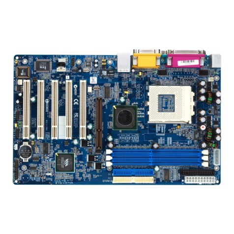
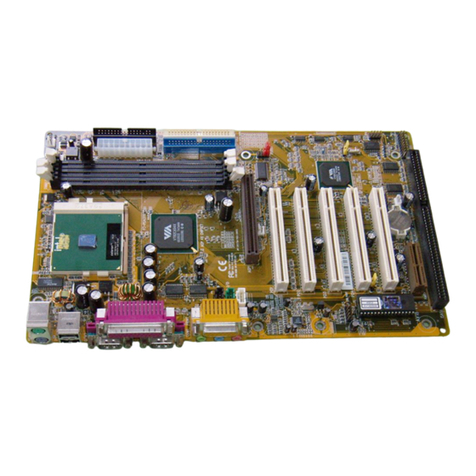
Shuttle Spacewalker HOT-685 User manual

HOT-685
PPGACeleronprocessor
Based AGPMAIN BOARD
User's Manual

- 2 -
Shuttle®SpacewalkerTM HOT-685
PPGA Celeron®processor based AGPset Mainboard
Manual Version 1.0
Copyright
Copyright©1999 by Shuttle®Inc. All Rights Reserved.
No part of this publication may be reproduced, transcribed, stored in a retrieval system,
translated into any language, or transmitted in any form or by any means, electronic,
mechanical, magnetic, optical, chemical, photocopying, manual, or otherwise, without
prior written permission from Shuttle®Inc.
Disclaimer
Shuttle®Inc. shall not be liable for any incidental or consequential damages resulting
from the performance or use of this product.
This company makes no representations or warranties regarding the contents of this
manual. Information in this manual has been carefully checked for reliability; however,
no guarantee is given as to the correctness of the contents. In the interest of continued
product improvement, this company reserves the right to revise the manual or include
changes in the specifications of the product described within it at any time without
notice and without obligation to notify any persion of such revision or changes. The
information contained in this manual is provided for general use by the customers.
Trademarks
Spacewalker is a registerred trademark of Shuttle Inc.
Intel, Celeron is a registered trademarks of Intel Corporation.
PC/ATX is a registered trademark of International Business Machines(IBM) Corporation
PS/2 is a registered trademark of IBM Corporation.
AWARD is a registered trademark of Award Software Inc.
Microsoft and Windows are registered trademarks of Microsoft Corporation.
General Notice: Other brand and product names used herein are for identification
purposes only and may be trademarks of their respective owners.
- 3 -
Federal Communicationsr Commission (FCC)
ComplianceNotice
This equipment has been tested and found to comply with the limits for a Class B digital
device, pursuant to Part 15 of FCC Rules. These limits are designed to provide reason-
able protection against harmful interference in a residential installation.
This equipment generates, uses and can radiate radio frequency energy. If not in-
stalled and used properly, in strict accordance with the manufacturer's instructions, may
cause harmful interference to radio communications. However, there is no guarantee
that interference will not occur in a particular installation. If this equipment does cause
interference to radio or television reception, which can be determined by turning the
equipment off and on, the user is encouraged to try to correct the interference by one or
more of the following measures :
Reorient or relocate the receiving antenna.
Increase the separation between the equipment and receiver.
Connect the equipment into an outlet on a circuit different from that to which the
receiver is connected.
Consult the dealer or an experienced radio/television technician for help and for
additional suggestions.
The user may find the following booklet prepared by the Federal Communications
Commission helpful "How to Identify and Resolve Radio-TV Interference Problems."
This booklet is available from the U.S. Government Printing Office. Washington, DC
20402, Stock 004-000-00345-4
CE Notice
This device complies with the requirements oof the EEC directive 89/336/EEC with
regard to EMC (Electromagnetic Compatibility). Following standards are applied to this
product, in order to achieve compliance with the EMC:
Immunity is in accordance with EN 50082-1 (1992).
Emissions are in accordance with EN 55022 (1987) Class B.

- 4 -
TABLE OFCONTENTS
CHAPTER 1INTRODUCTION .........................................................5
CHAPTER 2FEATURES ..............................................................6
Accessories of HOT-685 ................................................................................. 8
CHAPTER 3HARDWARE INSTALLATION ..........................................9
The Installation PPGA CeleronProcessor ....................................................... 9
Jumpers ........................................................................................................... 10
CPU Clock Speed and ratio Selection - JP2, J113 and JP9.............................. 10
Special Tip for User's Reference Only............................................................. 11
Clear CMOS - JP8........................................................................................... 11
Flash EEPROM Vpp - JP7 .............................................................................. 11
Keyboard & PS/2 Mouse Power-on Setting - JP1 ........................................... 11
AT and ATX Power Supply Connectors Setting - J112................................... 12
On Board Audio Controller Setting - JP6 ........................................................ 12
Connectors ...................................................................................................... 13
CHAPTER 4MEMORY CONFIGURATION ..........................................18
CHAPTER 5FLASH UTILITY ........................................................19
CHAPTER 6 AWARD BIOSSETUP ...............................................21
The Main Menu............................................................................................... 22
Standard CMOS Setup .................................................................................... 24
BIOS Features Setup ....................................................................................... 26
Chipset Features Setup .................................................................................... 29
Power Management Setup ............................................................................... 32
PNP/PCI Configuration Setup ......................................................................... 35
CPU Features Setup ........................................................................................ 37
IntegratedPeripherals...................................................................................... 39
PasswordSetting ............................................................................................. 43
T
T

- 5 -
INTRODUCTION
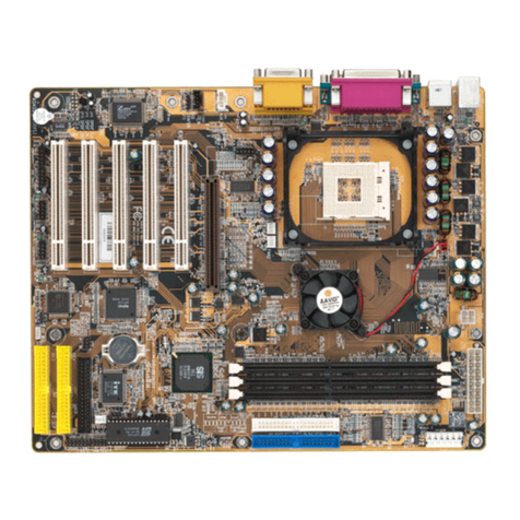
HOT-685 is a highly integrated IBM PC/AT compatible system board designed
to meet the industry's most demanding desktop applications.
Based on the Intel 82443BX AGPset chipset which support up to 500MHz PPGA
Celeron processor with MMX technology.
HOT-685 is equipped with an Accelerated Graphics Port (A.G.P.), a high-perfor-
mance interconnect for graphic-intensive application, such as 3D applications.
The A.G.P. is independent of the PCI bus and is designed to exclusively use with
graphical-display devices. The HOT-685 supports 3.3V A.G.P. devices with data
transfer rates up to 133 MHz, allowing data throughput of 500 MB/sec.
The Intel's 82443BX AGPset chipset provides an integrated Bus Mastering IDE
controller with two high performance IDE interfaces which allows up to four IDE
devices connection and up to 33 MB/sec of data transfer rates.
Onboard FM801 is an advanced PCI audio controller, it is compatible with
Microsoft Windows, DirectX and Adlib Music Synthesizer, Sound Blaster Pro
and supports thousands of DOS games.
The on-board I/O controller provides standard PC I/O functions:
floppy drive interface, two FIFO serial ports, an InDA device port and a SPP/
EPP/ECPcapable parallel port.
HOT-685 is built with four PCI local bus slots providing a high bandwidth data
path for data-movement intensive functions such as graphics, and with one ISA
slot.
HOT-685 provides the foundation for cost effective, high performance and highly
expandable platforms, which delivers the latest in the Intel PPGA Celeron pro-
cessor and new advanced chipset technology.
1
1

- 6 -
FEATURES
The HOT-685 Mainboard is carefully designed for the demanding PC user who
wants high performance and many intelligent features in a compact package:
Chipset:
Features Intel's 440BX AGPset with I/O subsystems.
CPU Support:
Intel PPGA Celeron processor 300 ~ 500 MHz.
Versatile Memory Supports:
Supportsthree banks of normal or PC/100 SDRAMmaximum memory size up
to 768 MB.
PCI and ISA Expansion Slots:
Provides four 32-bit PCI slots and one 16-bit ISA slot.
Onboard I/O:
Provides one Floppy port; one AT keyboard and one PS/2 mouse Header connector
or one PS/2 mouse and one PS/2 Keyboard port connector; two high-speed UART
compatible serial ports and one parallel port with ECP and EPP capabilities. Serial
Port 2 can also be directed from COM2 to the Infrared Module for wireless connec-
tions.
Onboard PCI Bus Master IDE Controller:
Two Ultra DMA/33 Bus Dual-channel Master IDEports provide support to a
maximum offour IDE devices(one Master and one Slave per channel). The IDE
Bus implements data transfer speeds of up to 33MB/sec IDE and also supports
Enhanced PIO Modes 3 & 4 and Bus Master IDE DMA Mode 2 devices.
Onboard 12-pin AT and 20-pin ATX Power Supply:
Provides AT and ATX Power connectors onboard, ATX power connector supports
soft-on/off function.
System BIOS:
Provides licensed Award V4.51PG BIOS on 2MB Flash EEPROM.
Supports Green PC, Desktop Management Interface (DMI) and bundled with NCR
SCSI BIOS.
ACPI:
SupportACPI (Advanced Configuration and Power Interface)function. ACPI
provide more Energy Saving Features for the future operating system supporting
OS Direct Power Management (OSPM) functionality.
2
2

- 7 -
Board Size:
AT form factor, dimension 220mm x 230mm.
Advanced Features:
Low EMI --Using built-in Spread Spectrum with 1.5% modulation and automatic clock shut-
off of unused PCI/SDRAMS slots to reduce the Electromagnetic Interference (EMI).
Dual Function Power Button (ATX power only)-- The system can be one of two states, one
is Suspend mode and the other is the Soft-off mode. Pushing the power button for less than 4
seconds will place the system into Suspend mode. When push the power button for more than 4
seconds, the system enters the Soft-off mode.
Wake-On-LAN --The Wake-On-LAN connector onboard can be attached to a network card
that supports this function to wake up the system via the LAN.
(This function support Intel LAN card only).
Modem Ring Power-on --The system can be powered on automatically by activation of
modem ring.
PS/2 Keyboard & Mouse Power-on --The system will power-on automatically by stroke
keyboard or double click PS/2 mouse.
Optional Features:
Voltages Monitoring-- Various voltages of key elements, such as the CPU, and other critical
system voltage levels are monitored to ensure stable current reach to mainboard components.
System voltages include VCORE/VL2 on CPU, and +5V, +12V, -5V, -12V on system.
FAN Status Monitoring-- To prevent CPU overheat, CPU fans is monitored for RPM and
failure. (CPU Cooling FAN with RPM sensor is required)

- 8 -
ACCESSORIES OF HOT-685

- 9 -
The Installation PPGA Celeron Processor
HOT-685 mainboard provides a 370-pin ZIF Socket370 for Intel PPGA Celeron CPU.
The CPU that came with the mainboard should have a fan attached to it to prevent over-
heating. If this is not the case then purchase a fan before you turn on your system.
To install a CPU, first turn off your system and remove its cover. Locate the ZIF
Socket370 and open it by first pulling the lever sideways away from the socket then
upwards to a 90-degree right angle. Insert the CPU with the correct orientation as
shown.(Figure 3-1) Use the notched corner of the CPU as your guide. The notched corner
should point towards the end of the lever. Notice that there are two blank area where one
hole is missing from that corner of the square array of pin holes. Because the CPU has a
corner pin for two of the four corner, the CPU will only fit in the one orientationn, hold
down on the CPU and close the socket’s lever.
HARDWARE INSTALLATION
3
3
Then you should have a CPU fan that will
cover the face of the CPU. Apply thermal
jelly to the CPU metallic top and then
install the fan onto the CPU. (Figure 3-2 )
Figure 3-2
Figure 3-1

- 10 -
Jumpers
Several hardware settings are made through the use of jumper caps to connect jumper pins
on the main board. The jumper's pin 1 on main board will be on the top or on the left
when holding the main board with the keyboard connector away from yourself.
Jumpers with two pins will be shown as for Close (On) and for Open (Off).
To connect the pins, simply place a plastic jumper cap over the two pins.
CPU Clock Speed and ratio Selection - JP2, J113 and JP9
HOT-685 mainboard features a clock generator to provide adjustable system clock
frequency. Jumpers JP2 and J113 determine the system clock frequency 66MHz to
150MHz. and JP9 is a 8-pin jumper which determine the processor clock ratio from
2X to 8X.
Figure 3-3 shows the position of JP2, J113
and JP9 on the mainboard.
Table 3-1 shows adjustable System clock
on jumper JP2 and J113.
Table 3-2 shows adjustable CPU Clock
Ratio on jumper group JP9.
Figure 3-3
Note:Present PPGA Celeron CPU Clock ratio
is fixed and unable to adjust, for those processors,
JP9 is not functional.
CPU
HostClock JP2and J113
66 MHz
75 MHz
83 MHz
100 MHz
103 MHz
112 MHz
124 MHz
133 MHz
140 MHz
150 MHzTable 3-1
CPU
Clock RatioJP9CPU
Clock RatioJP9
2x5.5x
(366 /66 )
2.5x6x
(400 /66 )
3x6.5x
(433 /66 )
3.5x
(350 /100 )7x
(466 /66 )
4x
(400 /100 )7.5x
(500 /66 )
4.5x
(300 /66 )
(450 /100 )8x
5x
(333 /66 )
(500 /100 )
Table 3-2

- 11 -
Special Tip for User's Reference Only
HOT-685 mainboard provides a special Jumper
J10 to overspeed your 66 MHz based Intel PPGA
Celeron processor to 100 MHz.
Normally, CPU Host Clock 100 ~ 150 MHz are
not available for 66 MHz based processor.
But, when pull out mini jumper from J10 (let it
open), the user can Hard-Configure your 66 MHz
based processor to 100 MHz based. For example,
overspeed your 333 MHz (66 MHz x 5) PPGA
Celeron to 400 MHz (100 x 4) or more.
Figure 3-4
K/B & PS/2 Mouse Power-On Setting - JP1
HOT-685mainboard provides an optional power-on
function by stroke any key (or hot-key) on keyboard
or double click on PS/2 mouse.
Note: Power-on by serial mouse is not supported
JP1 is the jumper used to set the functions of keyboard
& PS/2 mouse power-on Enabled or Disabled.
When you enabled K/B & PS/2 Mouse Power-ON
function, you also have to set the proper item on
POWERON function category of Integrated
Peripheralsof BIOS setup.
Flash EEPROM Vpp - JP7
HOT-685 mainboard supports two types of Flash EEPROM : 5 volt and 12 volt. By
setting up jumper JP11, the main board can use both 5V or 12V flash EEPROM with new
system BIOS files as they come available.
JP7 Pin 2-3 Close for
12V Flash EEPROM JP7 Pin 1-2 Close for
5V Flash EEPROM
K/B&PS/2Mouse Power-OnJP1
Keyboard &
PS/2 Mouse
Power-On
Disabled
Keyboard &
PS/2 Mouse
Power-On
Enabled
PS/2 Mouse
Power-On
Enabled
Keyboard
Power-On
Enabled
Table 3-3
Clear CMOS - JP8
HOT-685mainboard supports jumper JP8for
dischargingmainboard's CMOS memory.
This jumper can clear the CMOS data stored in
the I/O chip. To clear the CMOS data please
follow listed steps:
1) Turn off the PC,
2) Remove mini jumper from JP8 pin 1-2,
3) Insert mini jumper to JP8 pin 2-3 for a brief while,
4) Remove mini jumper from JP8 in 2-3,
5) Reinsert mini jumper to JP8 pin 1-2,
6) Turn on the PC.

- 12 -
AT and ATX Power Supply Connectors Setting - J112
The mainboard provides both 12-pin AT type
and 20-pin ATX type power supply connectors.
Jumper J112 is used to set which type of power
supply is used.
J112 Close (On) for AT Power Connector.
J112 Open (Off) for ATX Power Connector.
On Board Audio Controller Setting - JP6
HOT-685mainboard provides on-board PnP
64 voices wavetable sound chip which based
on FortéMedia PnP 3D integrated audio
controllerchip.
Jumper JP6 is used to enable or disable it.
JP6 Pin 1-2 Close (On)
On-boardAudio Controller Enabled (default)
JP6 Pin 2-3 Close (On)
On-board Audio Controller Disabled
Figure 3-5
Figure 3-6

- 13 -
Connectors
Front Panel Connectors (JP10)
Speaker Connector - SPKER
PC speaker connector may attach a 4-pin PC speaker cable from the case to this connector.
HDD LED Connector - HDD-LED
Attach a 2-pin IDE drive LED cable to this connector. The LED lights when an IDE
device is active.
ATX Power On/Off Switch Connector - PW-ON
Attach a 2-pin momentary type switch to this connector for turning on or off your ATX
powersupply.
Hardware Reset Connector - RESET
Attach 2-pin hardware reset switch to it. Closing the reset switch causes the system to restart.
PW-LED Connector - PWR-LED
Attach 3-pin Power-LED connector cable from the housing front panel to PW-LED header
on the mainboard. The power LED stays lights while the system is running.
EPMI Connector - EPMI
Hardware System Management Interface connector may attach a 2-pin momentary switch
to it. When push it will force system get into power saving mode, and the system will
resume when switch is pushed again.
Green LED Connector - GLED
Attach a 2-pin Green LED cable to it. The Green LED lights when the system get into
power saving mode. The Green LED off when the system resume back to normal mode.
Figure 3-7

- 14 -
Figure 3-10 :
ATX Power Supply Connector
Figure 3-9 :
AT Power Supply Connector
Other Connectors
AT and ATX Power Supply Connectors
AT Power Connector is a 12-pin male header
connector. Plug the connector from the power
directly onto the board connector while making
sure the pin 1 is in its position. The main board
requires a power supply with at least 200 watts
and"power good signal".
Figure 3-9 shows AT Power Supply Connector.
ATXPowerConnector is a 20-pin male header
connector is connecteed to the ATX power supply.
The plug of the power supply will only insert in
one orientation because of the different hole shade
and size. Find the proper orientation and push
down firmly making sure that the pins are aligned.
Figure 3-10 shows ATX Power Supply Connector.
IR Connector - J18
If you have an Infrared device, this mainboard can
implementIR(Infrared)transfer and meetbothASKIR
and HPSIR specifications. To enable the IR transfer
function, follow these steps:
Step1. Attach the 5-pin infrared device cable to J18
connector.(Referto the above diagram for IR
pinassignment.)
Step2. Configure the Infrared transfer mode in the
UR2 Mode field of Integrated Peripherals
menu in BIOS Setup. This mainboard sup-
ports IrDA 1.0, ASKIR, MIR 0.57M and
MIR 1.15M transfer modes. FIR is not cur-
rentlysupported.
Figure 3-8
Figure 3-11 :shows J18's pin assignment.

- 15 -
Figure 3-12
AT Keyboard & PS/2 Mouse Header or
PS/2 Keyboard & PS/2 Mouse Connector
ATKeyboard &PS/2Mouse Header:
One 5-pin female AT keyboard & one 5-pin PS/2 mouse
header is located at the rear of the main board.
The main board provides a 5-pin PS/2 mouse header for
an optional PS/2 mouse cable. Figure 3-13 on the right
side indicates the pinout of pin header.
PS/2Keyboard & PS/2MouseConnector:
Two 6-pin female PS/2 keyboard & Mouse Connectors
is located at the rear of the main board. PS/2 Mouse on
top of connector and PS/2 Keyboard on the bottom of
connector. Plug the PS/2 keyboard and mouse jack into
thisconnector.
Caution : When a PS/2 mouse adapter cable is used,
make sure connect PS/2 mouse adapter cable hole 1 to
the pin 1 of onboard PS/2 connector (J109). Reversed
connecting may cause damage to your PS/2 mouse.
USB Port Connectors
The mainboard provides two sets of USB (Universal
Serial Bus) connector - J108
CPU, Chassis & AGP cooling Fan
connectors - JP5, JP3 & J1
The main board provides three onboard 12V cooling
fan power connectors. Depending on the fan maker,
the wiring and plug may be different. The red wire
should be connected to +12V and black wire should
beconnected to ground (GND).
Wake-On-LAN Connector - J14
Attach a 3-pin connector from the LAN card which
supports the Wake-On-LAN (WOL) function. This
function lets users wake up the connected system
through the LAN card.
SB-Link connector - JP40
The main board provides a 2x3 pin SB-Link header
accepts the Creative CT4600 series PCI sound cards
with PCI solution to connect the legacy Sound Blaster
compatible audio to the PCI bus.
Figure 3-14
Figure 3-13

- 16 -
IDE, Floppy, Parallel and Serial port
connectors
The mainboard package has included one 40-pin ribbon
cable for IDE H.D.D, one 34-pin ribbon cable for F.D.D,
one 25-pin ribbon cable for printer and two 9-pin ribbon
cables for COM port devices. Flat cables should be
connected with the red stripe on the pin 1 side of the
conector.
Game / MIDI and SPK-OUT / Line-IN /
Mic-In connectors
Themainboard package included a Game/Audio connect-
ing adapter for connecting Joystick/MIDI device and
Audio input/output devices.
J7 and J111 connectors which use to connect attachement
Game/Audio connecting adapter. 10-pin flat cable of
adapter connect to J111 and 15-pin flat cable connect to
J7 on the mainboard. Flat cables should be connected
with the red stripe on the pin 1 side of the conector.
GAME/ MIDI
The Game/MIDI port is a 15-pin female connector.
This port can be connected to any IBM PC compatible
joystick with a 15-pin D-sub connector.
MIDIInstrumentConnection
You need a MIDI adapter to connect a MIDI instru-
ment to the mainboard. The MIDI adapter can be con
nected to the GAME/MIDI port. You will also need
MIDI sequencing software to run MIDI instruments
with your computer.
SPKOUT
SPK OUT is a stereo output through which the com-
bined signal of all internal and external audio sources
on the board is output. It can be connected to 1/8-inch
TRS stereo headphones or to amplified speakers.
LINE-IN
LINE-IN is a stereo line-level input that accepts a 1/8-
inch TRS stereo plug. It can be used as a source for
digital sound recording, a source to be mixed with the
output, or both.
MIC-IN
MIC-IN is a 1/8-inch jack that provides a mono input.
It can use a dynamic mono or stereo microphone with
a resistance of not more than 600 ohms.
Figure 3-15
Figure 3-16 : Game/Audio
Connecting adapter.

- 17 -
TAD
Port SJ2 can be used to connect a modem audio line
to HOT-685. You would use this connector when
telephone answering machine software for input and
output.
SJ2 (TAD) pin assignment :
4 = MONO
3 = Ground
2 = Ground
1 = PHONE
CD-IN
Port SJ1 is used to attach a CD-ROM audio connector.
SJ1 (CD_IN) pin assignment :
4= Right Channel
3 = Ground
2 = Ground
1 = Left Channel
Figure 3-17

- 18 -
MEMORY CONFIGURATION
4
4
The HOT-685 mainboard provides three 168-pin DIMM sockets that make it
possible to install from 8MB up to 768MB of SDRAM. The DIMM socket
support 8MB, 16MB, 32MB, 64MB, 128MB and 256MB 3.3V single- or double-
side SDRAM DIMM.
The three DIMM sockets are arranged in three banks of one socket each. Each
bank provides a 64/72-bit wide data path.
HOT-685 provides optional data integrity features including EC (Error Checking)
in the memory array. EC mode provides single and multiple bit error detection.
TheHOT-685 provides error checking and correction ofthedata.
Install memory in any or all of the banks in any combination as follows:
Figure 4-1
DIMM
SocketMemoryModulesMudule
Quantity
DIM1A8MB,16MB,32MB,64MB,128MB,256MB
168-pin3.3VSDRAMDIMM x1
DIM2A8MB,16MB,32MB,64MB,128MB,256MB
168-pin3.3VSDRAMDIMM x1
DIM3A8MB,16MB,32MB,64MB,128MB,256MB
168-pin3.3VSDRAMDIMM x1
Table 4-1

- 19 -
5
5FLASH UTILITY
This chapter briefly discusses Award Flash utility in order to guide you through
updating your old BIOS. The file name we use to program here is test.bin, and
the file name to save old BIOS is 685.OLD. Please note that those file names are
not absolute. They are only examples to let you have a more clear understanding
of the updating process.
How to Begin
1. Please type “awdflash” and press the ENTER key to begin the updating
process.
2. Once you enter, you will see a main menu displaying:
3. Move the cursor to “File Name to Program: ”
4. Type the program name “test.bin”, and then press the ENTER key.
5. At the bottom of the menu, you will be requested to answer:
“Do You Want to Save BIOS (Y/N)? ”
The following manual is intended to guide you through the process of both “No”
and “Yes” cases respectively.
If “No”
If you do not wish to save the old BIOS:
1. Please type “N”, and then press the ENTER key.
2. Then you will be requested to answer:
“Are You Sure to Program? “
3. Answer “N” if you do not want to program, and then it will exit.

- 20 -
If “Yes”
To save the old BIOS:
1. Please respond “Y”, and then press the ENTER key.
2. Move the cursor to “File Name to Save: “
3. Type file name “TEST.BIN”, and then press the ENTER key. (Your old BIOS
will be saved in the file name you create. In this case, the old BIOS is saved
in the file name, 685.OLD).
4. Then you will be requested to answer:
“Are You Sure to Program (Y/N)? “
5. Type “Y” to begin programming, and press the ENTER key.
6. When the programming is finished, the showing message will appear:
7. Once you see the showing message “Power Off or Reset System”,
please restart your system.
8. When you power on the computer again, you will find your old BIOS has
already been successfully updated.
To view a complete usage of FLASH utility, please type “awdflash /?” and
press the ENTER key.
Notes About Award Flash Utility
Please note that Award Flash Utility cannot run under EMM386or QEMM.
Thus, when executing the command “awdflash”, an error message will appear:
“Error Message: Fail — Due to EMM386 or QEMM !”
Table of contents
Other Shuttle Computer Hardware manuals

Shuttle
Shuttle PCL71 User manual

Shuttle
Shuttle WWN03 Installation instructions

Shuttle
Shuttle MN31L User manual

Shuttle
Shuttle MS52PN User manual

Shuttle
Shuttle DH610S Series User manual

Shuttle
Shuttle D230 User manual

Shuttle
Shuttle DS81 Series User manual

Shuttle
Shuttle AK38 User manual

Shuttle
Shuttle WLN-M User manual

Shuttle
Shuttle WLN-M Installation instructions