Singmai Electronics PT9 User manual

SingMai Electronics
PT9 User Manual Revision 0.3Page 1 of 38
PT9
Multi-standard
Video Encoder
with cross-colour reduction
User Manual
Revision 0.3
9th June 2018

SingMai Electronics
PT9 User Manual Revision 0.3Page 2 of 38
Revisions
Date
Revisions
Version
19-11-2015
First draft.
0.1
29-08-2017
Revisions to comb filter.
Cross-colour reduction description added.
Pre-emphasis added.
Cross luma reduction removed.
Additions to technical description.
0.2
09-06-2018
Minor correction to Table 8.
0.3

SingMai Electronics
PT9 User Manual Revision 0.3Page 3 of 38
Contents
Revisions .................................................................................................................................................. 2
Contents...................................................................................................................................................3
Tables .......................................................................................................................................................3
Figures...................................................................................................................................................... 3
1. Introduction ...................................................................................................................................5
2. PT9 Module description.................................................................................................................6
3. Signal Interconnections.................................................................................................................7
4. Signal Levels...................................................................................................................................9
5. Test signals................................................................................................................................... 10
6. Technical Overview....................................................................................................................... 11
PT9_encoder.v................................................................................................................................... 11
PT9_Register_control.v..................................................................................................................... 11
PT9_BT656_receiver.v....................................................................................................................... 11
PT9_SPG.v .......................................................................................................................................... 11
PT9_Subcarrier_gen.v .......................................................................................................................12
PT9_Chroma_modulator.v................................................................................................................12
PT9_ROM.v ........................................................................................................................................12
PT9_output_proc.v............................................................................................................................12
PT9_Comb_filter.v............................................................................................................................ 14
ram_infer_generic.v ......................................................................................................................... 14
7. Cross-colour reduction .................................................................................................................15
8. Register interface ........................................................................................................................ 19
9. Register descriptions ...................................................................................................................20
10. Horizontal timing registers ...................................................................................................... 23
11. Default Register Settings............................................................................................................. 25
12. Interfacing to a DAC..................................................................................................................... 27
13. Specification .............................................................................................................................28
14. Measurements..........................................................................................................................29
Tables
Table 1 PT9 Altera FPGA resource requirements ...................................................................................5
Table 2 PT9 module heirachy. .................................................................................................................6
Table 3 Input/Output signals...................................................................................................................7
Table 4 BT656 Signal Levels....................................................................................................................9
Table 5 BT656 test waveform (525 line)............................................................................................... 10
Table 6 BT656 test waveform (625 line) .............................................................................................. 10
Table 7 Register descriptions................................................................................................................ 22
Table 8 Default Register settings .........................................................................................................26
Table 9 PT9 Specifications. ...................................................................................................................28
Figures
Figure 1 PT9 Interconnection diagram. ..................................................................................................7
Figure 2 CVBS output levels ...................................................................................................................9
Figure 3 PT9 Block Diagram. .................................................................................................................. 11
Figure 4 Chroma modulation filter. .......................................................................................................12
Figure 5 Luma interpolation filter frequency response........................................................................13
Figure 6 Sinx/x filter frequency response. ............................................................................................13
Figure 7 NTSC Pre-emphasis filter......................................................................................................... 14
Figure 8 PAL pre-emphasis filter........................................................................................................... 14

SingMai Electronics
PT9 User Manual Revision 0.3Page 4 of 38
Figure 9 PAL frequency spectrum .........................................................................................................15
Figure 10 Zone plate image after line comb decoding. ....................................................................... 16
Figure 11 Zone plate image after frame comb decoding. .....................................................................17
Figure 12 Zone plate image, line comb decoded from PT9 encoder................................................... 18
Figure 13 NTSC zone plate with line comb decoder. Left: conventional encoder/line comb decoder.
Right: PT9 encoder with conventional line comb decoder. ................................................................ 18
Figure 14 Control interface Timing........................................................................................................ 19
Figure 15 NTSC horizontal timing.......................................................................................................... 23
Figure 16 PAL-BG horizontal timing ......................................................................................................24
Figure 17 Interfacing to a DAC............................................................................................................... 27
Figure 18 NTSC Vertical blanking interval .............................................................................................29
Figure 19 NTSC Horizontal Timing.........................................................................................................30
Figure 20 NTSC 75% Colour bar..............................................................................................................30
Figure 21 NTSC Chroma/Luma delay ......................................................................................................31
Figure 22 NTSC K Factor .........................................................................................................................31
Figure 23 NTSC Multiburst (No sinx/x correction) ............................................................................... 32
Figure 24 NTSC Noise Spectrum (Black)............................................................................................... 32
Figure 25 NTSC Noise Spectrum (luma ramp)......................................................................................33
Figure 26 PAL Vertical blanking interval...............................................................................................33
Figure 27 PAL Horizontal timing ...........................................................................................................34
Figure 28 PAL 75% Colour bars ..............................................................................................................34
Figure 29 PAL Chroma/Luma delay.......................................................................................................35
Figure 30 PAL K-factor........................................................................................................................... 35
Figure 31 PAL Multiburst (no sinx/x correction)...................................................................................36
Figure 32 PAL Noise spectrum (black).................................................................................................. 37
Figure 33 PAL Luma non-linearity .........................................................................................................38

SingMai Electronics
PT9 User Manual Revision 0.3Page 5 of 38
1. Introduction
PT9 is a broadcast quality, multi-standard, video encoder supporting PAL-M/N/B/D/G/H/I and NTSC-
M/J outputs.
The intellectual property block accepts BT656 formatted data, in either 8 or 10 bit format, with the
associated 27MHz clock, and it encodes this data to a 10 bit, digital composite video output at
27MHz, which can be used to directly drive a digital to analogue converter, modulator or other
output device.
PT9 includes special cross-colour reduction circuitry, particularly of help in reducing artifacts when
used with a line comb video decoder.
The encoder can also be set to a free-run mode in which it ignores the BT656 timing information
and data and uses the clock input to generate a black and burst output.
Control and status registers are written to and read from using a conventional 8 bit wide
microprocessor interface.
The Altera FPGA usage (taken from the SM05 evaluation board compilation statistics) is shown in
Table 1.
Logic Elements
Memory Bits
M9K blocks
9x9 Multipliers
18x18 multipliers
9323
218112
25
1
41
Table 1 PT9 Altera FPGA resource requirements
The ASIC equivalent gate count is approximately 112k gates. The memory constitutes:
1 512 x 24 = 12288 bit single port ROM
4 2048 x 11 bit single port RAM = 90112 bits.
2 2048 x 10 bit single port RAM = 40960 bits.
2 2048 x 9 bit single port RAM = 36864 bits.
2 2048 x 12 bit single port RAM = 49152 bits.

SingMai Electronics
PT9 User Manual Revision 0.3Page 6 of 38
2. PT9 Module description
The PT9 encoder comprises 10 Verilog modules. PT9_encoder.v is the top level module of the
hierarchy; six of the other modules are instantiated from it.
Top level
2nd level
3rd level
4th level
PT9_encoder.v
PT9_Register_control.v
PT9_BT656_receiver.v
PT9_SPG.v
PT9_Subcarrier_gen.v
PT9_ROM.v
PT9_Chroma_modulator.v
PT9_output_proc.v
PT9_Comb_filter.v
ram_infer_generic.v
Table 2 PT9 module heirachy.

SingMai Electronics
PT9 User Manual Revision 0.3Page 7 of 38
3. Signal Interconnections
The PT9 signal interconnect diagram is shown in Figure 1.
Figure 1 PT9 Interconnection diagram.
The signal descriptions are shown in Table 3, below.
Signal
Description
Clock
27MHz clock input synchronous with the BT656 input data. The BT656
data should be stable at the rising edge of this clock.
Clock2x
54MHz clock input (2x Clock). The rising edge of this input should be
synchronous with the rising edge of Clock. This clock is used for the
single port RAM.
BT656_data[9..0]
BT656 compliant input data, sampled on the rising edge of Clock. If the
input is 8-bit the bottom 2 bits should be connected to ground (logic
‘0’).
RESETn
Asynchronous active low reset signal. Asserting this input sets all the
control registers to their default value and resets all registers.
A[5:0]
Control address bus input used to select the control register to be
written to/read from.
Din[7:0]
Control data input bus.
PT9_CSn
Control chip select input, active low. Used in combination with the WRn
input to control writing to the control registers.
PT9_WRn
Active low write enable input. Used in combination with the CSn input
to control writing to the control registers.
PT9_Register_out[7:0]
Control output data bus. Outputs the control/status register data
selected by the A[5:0] bus.
CVBS_out[9..0]
The digital composite output. The output format is straight binary with
bit 9 being the MSB. The output is valid on the rising edge of the Clock
input.
Comp_Sync
Composite sync signal output.
Table 3 Input/Output signals

SingMai Electronics
PT9 User Manual Revision 0.3Page 8 of 38
The Verilog instantiation of PT9 is shown below:
// Instantiate Video encoder (PT9_encoder)
PT9_encoder PT9_encoder_inst
(
.Clock(Clock_sig) , // input Clock_sig
.Clock2x(Clock2x_sig) , // input Clock2x_sig
.BT656_data(BT656_data_sig) , // input [9:0] BT656_data_sig
.RESETn(RESETn_sig) , // input RESETn_sig
.A(A_sig) , // input [5:0] A_sig
.Din(Din_sig) , // input [7:0] Din_sig
.PT9_CSn(PT9_CSn_sig) , // input PT9_CSn_sig
.PT9_WRn(PT9_WRn_sig) , // input PT9_WRn_sig
.PT9_Register_out(PT9_Register_out_sig) , // output [7:0] PT9_Register_out_sig
.CVBS_out(CVBS_out_sig) , // output [9:0] CVBS_out_sig
.Comp_Sync(Comp_Sync_sig) // output Comp_Sync_sig
);
SingMai Electronics
PT9 User Manual Revision 0.3Page 9 of 38
4. Signal Levels
The expected signal levels for the BT656 input are shown in Table 4, below.
10-bit YCbCr signal Levels 100/0/100/0
Y
Cb
Cr
White
940
512
512
Yellow
840
64
585
Cyan
678
663
64
Green
578
215
137
Magenta
426
809
887
Red
326
361
960
Blue
164
960
439
Black
64
512
512
10-bit YCbCr signal Levels 75/0/75/0
Y
Cb
Cr
White
940
512
512
Grey
721
512
512
Yellow
646
176
567
Cyan
525
625
176
Green
450
289
231
Magenta
335
735
793
Red
260
399
848
Blue
139
848
457
Black
64
512
512
Table 4 BT656 Signal Levels
The resulting nominal output levels for a 100% PAL colour bar input are shown in Figure 2.
Figure 2 CVBS output levels

SingMai Electronics
PT9 User Manual Revision 0.3Page 10 of 38
5. Test signals
The PT9 is supplied with BT656 test waveforms to facilitate testing and verification.
The waveforms are supplied as Excel spreadsheets and are 75% saturation colour bars. Other
waveforms can be supplied on request for a small charge.
There are four elements to the complete frame of video and each element consists of 1716 (515
line) or 1728 (625 line) samples in a multiplexed Cb,Y,Cr,Y sequence. Each sample of each element
should be clocked at 27MHz.
For 525 line standards the elements should be selected according to the following table:
Line No.s
Pattern
Element
4-19, 264, 265
F0V1
1
1-3, 266-282
F1V1
2
20-263
75% Bars F0
3
283-525
75% Bars F1
4
Table 5 BT656 test waveform (525 line)
For 625 line standards the elements should be selected according to Table 6.
Line No.s
Pattern
Element
1-22, 311, 312
Fsync F1
1
313-335, 624, 625
Fsync F2
2
23-310
75% Bars F1
3
336-623
75% Bars F2
4
Table 6 BT656 test waveform (625 line)

SingMai Electronics
PT9 User Manual Revision 0.3Page 11 of 38
6. Technical Overview
A simplified block diagram of the PT9 PAL encoder is shown in Figure 3.
Figure 3 PT9 Block Diagram.
The following is a brief description of the PT9 modules.
PT9_encoder.v
The top level module provides the interconnections to the other modules in the IP core.
PT9_Register_control.v
This module provides the register interface for the PT9. Chapter 8 provides a description of the
interface and Chapter 9 provides a description of the registers.
PT9_BT656_receiver.v
The input to the encoder is an 8 or 10 bit BT656 formatted data stream and associated 27MHz
clock. If the input is 8 bits the bottom 2 bits should be tied to logic ‘0’.
The 656 interface block identifies and extracts the TRS codes from the stream and de-multiplexes
and co-times the Y,Cb,Cr data.
This module also detects the line standard of the input BT656 video which can be used to auto
select the output video standard.
PT9_SPG.v
The clock, frame and active video signals from the BT656 receiver are used to synchronise a sync
pulse generator (SPG). The principal purpose of the SPG is to generate a compatible composite
sync output but it also generates the PAL switch signal (7.8kHz), the Bruch Blanking sequence for
PAL burst blanking, the Burst gate signal for inserting the colour burst into the output data and
the video blanking pulse.

SingMai Electronics
PT9 User Manual Revision 0.3Page 12 of 38
PT9_Subcarrier_gen.v
The input clock drives a 32-bit ratio counter which generates a precise subcarrier frequency for the
selected standard. An 11-bit phase word from this ratio counter addresses 12 bit wide Sin and Cos
look-up tables. To save on memory only one quadrant of the Sin and Cos tables are stored and the
addressing and data is modified to generate the other three quadrants.
The resulting Sin and Cos data is then multiplied by the U and V data during the active video period
and a shaped Burst Gate pulse is used to insert the colour burst.
The colour frame output of the SPG ensures the burst is correctly inhibited whilst the PAL switch
output of the SPG switches the 135deg and 225deg phase increments in the correct sequence. For
NTSC it is possible to add in a phase offset (hue).
PT9_Chroma_modulator.v
The Cb and Cr chroma from the BT656 receiver is interpolated from its 6.75MHz sample rate to the
27MHz output sample rate. The interpolation filter has a 1.3MHz (-3dB) frequency response with a
Gaussian response (see Figure 4).
Figure 4 Chroma modulation filter.
The filtered Cb and Cr signals are then scaled, multiplied by the sin and cos waveforms from the
subcarrier generator and added to generate a composite chroma signal. The resulting U.sin
(2πfsc.t) and V.cos (2πfsc.t) data is added together to create the chrominance signal which has
blanking added as well as programmable gain.
PT9_ROM.v
This module provides the 512 x 12 bit sine and cosine lookup tables for the subcarrier generator.
PT9_output_proc.v
The output processing module combines all the components of the video output into one
composite output signal.
The luma signal is interpolated from 13.5MHz to 27MHz –the filter response is shown in Figure 5.
The composite sync signal has an approximation to a 2T raised cosine wave shape added to ensure
rise/fall time conformance to the video specification.
The luminance signal is then passed to the comb filter module to provide the cross-colour
reduction. A description of this mode can be found in Chapter 7.
The luminance, chrominance and composite sync are then added together to generate the 10-bit
27MHz CVBS signal.
InphaseFilterFrequencyResponse
FrequencyinMHz
Magnitude
0 1 2 3 4 5 6 7 8
0.0
0.1
0.2
0.3
0.4
0.5
0.6
0.7
0.8
0.9
1.0

SingMai Electronics
PT9 User Manual Revision 0.3Page 13 of 38
Figure 5 Luma interpolation filter frequency response.
A switchable sinx/x filter allows compensation for the DAC sampling error. Its response is shown in
Figure 6.
Figure 6 Sinx/x filter frequency response.
The last block of the output-proc module is the pre-emphasis block. When driving long lengths of
cable with the PT9 there will be a high frequency loss. This is usually compensated for with a high
frequency boost network at the receiver (decoder). To provide better compensation the PT9 has a
pre-emphasis filter that is matched to response of typical coaxial cable (e.g. RG-59). The filter
provides a high frequency boost whose amplitude is controllable via a register. The response of
this filter is shown in Figures 7 and 8.
It is possible, when used with the SingMai video decoders, that this frequency compensation can
be automatic. Contact SingMai for more details.
InphaseFilterFrequencyResponse
FrequencyinMHz
Magnitude in dB
0 2 4 6 8 10
-60
-50
-40
-30
-20
-10
0
10
Inphase Filter FrequencyResponse
FrequencyinMHz
Magnitude in dB
0 2 4 6
0.0
0.4
0.8
1.2
1.6
2.0
2.4
2.8
3.2

SingMai Electronics
PT9 User Manual Revision 0.3Page 14 of 38
Figure 7 NTSC Pre-emphasis filter.
Figure 8 PAL pre-emphasis filter.
PT9_Comb_filter.v
The comb filter is used to reduce the components of the composite video that can cause artifacts
when decoded with a line comb video decoder. A description of its operation may be found in
Chapter 7. The comb filter module also provides compensating delays for the chroma components.
ram_infer_generic.v
This module is a generic single port RAM that is used in the comb filter module.
InphaseFilterFrequencyResponse
FrequencyinMHz
Magnitude in dB
0 1 2 3 4 5 6
-14
-12
-10
-8
-6
-4
-2
0
2
InphaseFilterFrequencyResponse
FrequencyinMHz
Magnitude in dB
0 1 2 3 4 5 6
-14
-12
-10
-8
-6
-4
-2
0
2

SingMai Electronics
PT9 User Manual Revision 0.3Page 15 of 38
7. Cross-colour reduction
When colour NTSC and PAL broadcasts were first introduced, to maintain compatibility with
monochrome TV transmissions and because of the restriction in the bandwidth available for
transmission, the chroma had to occupy the same frequency as the higher luma frequencies (see
Figure 9).
Figure 9 PAL frequency spectrum
The luma information occupies from 0 - 5.75MHz (in a studio environment –i.e. not for RF
broadcast) whereas the chroma information is modulated onto a subcarrier at approximately
4.43MHz with a 1.3MHz bandwidth (PAL standard). Therefore, at frequencies from approximately
3 –5.7MHz, the chroma and luma occupy the same spectrum.
It is the job of the video decoder to separate these two components.
To separate the luma from the composite signal we could employ a low pass filter that blocks all
frequencies above 3MHz. This will result in ‘clean’ luma (i.e. with no chroma crosstalk) but we have
reduced the luma bandwidth of the signal by nearly one-half. This approach is even more
detrimental for NTSC where the subcarrier is at 3.58MHz, still with a 1.3MHz bandwidth, so the
resulting luma bandwidth would be only 2.3MHz (although we do also get a small amount of the
very high frequencies, above 4.8MHz). We can improve the luma bandwidth by using a narrow
notch filter, centred on the subcarrier frequency, and allow a small amount of cross-talk at the
extremes of the chroma bandwidth but we are still removing a large part of the luma detail.
The chroma, once demodulated, will always contain high frequency luma. To reduce the
interference of the chroma information for monochrome TV receivers, the chroma subcarrier
frequency has a fixed phase relationship with respect to the horizontal line frequency. We can

SingMai Electronics
PT9 User Manual Revision 0.3Page 16 of 38
utilize this to help separate the chroma and luma where they overlap (the chroma information will
have this phase relationship, the high frequency luma information will not).
The PAL subcarrier is shifted 270° in phase every line of a field, so over a two lines of field it will be
180° phase shifted. If we add these two lines together it will cancel the chroma and reinforce the
luma. This ‘line-comb’ filter can recover the full luma bandwidth, but only under certain conditions.
If there is a vertical transition in the image (one line of one colour, another of a different colour)
then the line comb will fail (giving what are called, ‘hanging dots’). Similarly if there are diagonals
in the image then the line comb will fail. In each case the failure can result in higher levels of
chroma, giving the familiar shimmering cross-colour effects on high frequency luma structure, as
shown in Figure 10.
Figure 10 Zone plate image after line comb decoding.
To separate the luma and chroma almost perfectly, a frame comb decoder can be used. The 3D
frame comb decoder, because it is combing spatially aligned images, does not suffer from the
problems of the 2D line comb decoder (where the comb taps are separated by a number of lines).
This can be seen in the frame comb decoded image of the zone plate in Figure 11.

SingMai Electronics
PT9 User Manual Revision 0.3Page 17 of 38
Figure 11 Zone plate image after frame comb decoding.
Unfortunately it is not always possible to ‘afford’ a frame comb decoder, but it is possible to
improve the decoded image by processing the encoded image. If the luma and chroma are comb
filtered prior to being summed to form composite video, we can remove the frequencies that
cause the problems for the line comb decoder. Ideally the comb filter architectures for the
encoder and decoder should be matched, which is the case for the SingMai PT9 encoder and the
PT4 line comb decoder.
The line comb decoded image using this technique is shown in Figure 12.
As you can see, the cross-colour is almost completely removed compared with the image in Figure
10, yet, because only the high frequency luma is combed, we still preserve as much picture detail
as possible compared with, for example, a simple notch filter. Of course this solution is not a
panacea as there is some loss of resolution, but the image detail would have been masked by the
cross-colour.
Figure 13 shows the comparative images using an NTSC zone plate.
For those instances where a line comb decoder is the only option, the PT9 can make substantial
improvements in the perceived video image.

SingMai Electronics
PT9 User Manual Revision 0.3Page 18 of 38
Figure 12 Zone plate image, line comb decoded from PT9 encoder.
Figure 13 NTSC zone plate with line comb decoder. Left: conventional encoder/line comb
decoder. Right: PT9 encoder with conventional line comb decoder.
SingMai Electronics
PT9 User Manual Revision 0.3Page 19 of 38
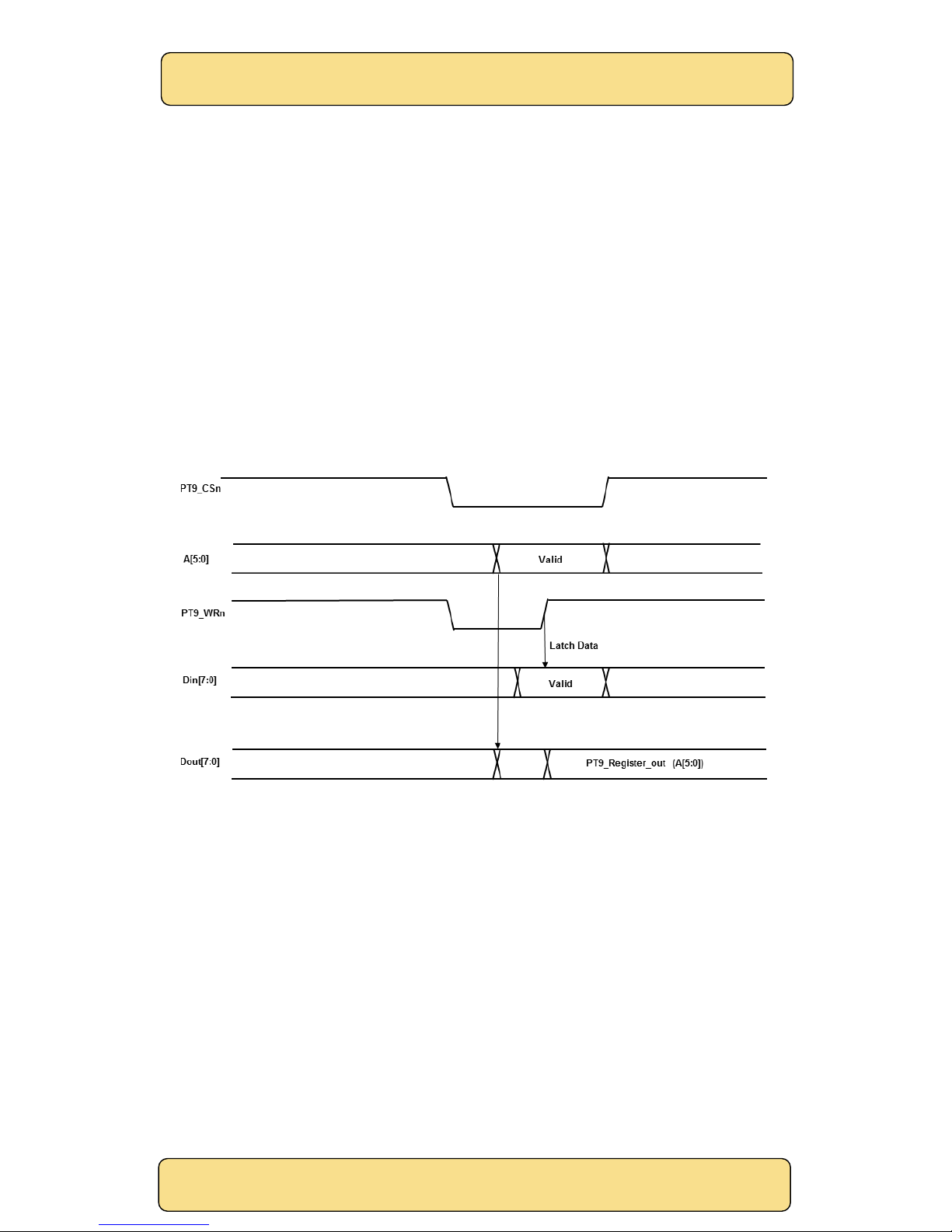
8. Register interface
Figure 14 shows the timing diagram for the register interface; it is a conventional microprocessor
interface. Each register is selected via a 6-bit address bus. Writes to unused register locations are
ignored.
To write to the selected register the PT9_CSn (chip select) input must be asserted low, A[5:0]
assigned the required register address and the data for this register set up. The PT9_WRn input
must then be driven low and high again: On the rising edge of this pulse the data is latched into
the address selected. The PT9_CSn should then be returned high.
For the write to occur reliably the address (A[5:0]) and data (Din[7:0]) must be stable and valid
during the low to high transition of the PT9_WRn pulse.
The address input also selects the register data that is presented on the PT9_Register_out[7:0]
bus. This output is independent of the PT9_CSn or PT9_WRn inputs.
Figure 14 Control interface Timing.

SingMai Electronics
PT9 User Manual Revision 0.3Page 20 of 38
9. Register descriptions
Table 7 lists all of the control and status registers. All of the registers are 8 bit wide although some
are concatenated together to create longer words. Unused register bits read back as zeros.
Note that, if Control Register bit 7 is asserted (Auto register = ‘1’), then the default values for
NTSC-M, PAL, PAL-M and PAL-N will be used by the PT9 and only the Control registers and the
pre-emphasis register will be active.
The default values are shown in Table 8. The registers may still be written to and read from in Auto
register condition.
Please note that some registers can be set to values that are illegal and will produce invalid
outputs.
Asserting the RESETn input sets the PT9 to Auto register and Auto standard.
Register
Offset
Register Name
R/W
Bit Value
Description
$00
Control 1
R/W
Control Register
7
Auto register. When set to ‘1’ preset values are used for PT9
register values and only the two control registers andpre-
emphasis register may be programmed (PAL/NTSC/PAL-M/PAL-N
standards only). When this bit is set to ‘0’ the programmable
register values are used for PT9 control, allowing the PT9 to be
programmed for other standards or custom modes. (Default value
= ‘1’).
6
Auto standard. Selects whether the output standard is selected
manually ( = ‘0’) via Bit 5 or via the line standard detection of the
BT656 input (525 or 625 line) (= ‘1’). (Default value = ‘1’).
5
If bit 6 = ‘0’ this bit selects the output line standard.
4
Selects either PAL/NTSC output (= ‘0’) or PAL-N/PAL-M output (=
‘1’).
5:4
Line standard detect (bit 6 =
‘1’) or bit 5 (bit 6 = ‘0’)
Bit 4
0
0
NTSC-M (Default)
0
1
PAL-M
1
0
PAL
1
1
PAL-N
3-0
Not used
$01
Control 2
R/W
Control/status register
7:6
Not used.
Sinx/x enable
5
If ‘0’the sinx/x DAC compensation filter is turned off. If ‘1’ it is
turned on. Default is ‘1’.
Luma comb
enable
4
If ‘1’ the luma data is combed to reduce cross-colour in the video
decoder. If ‘0’ the luma comb filter is bypassed. (Default = ‘1’)
Chroma_off
3
Turns off the colour modulator if set to ‘1’ (forces monochrome
output). (Default = ‘0’)
VBI_Pass
2
If 0 the vertical blanking is from lines 623.5-23.5 and lines 311-335
for PAL and lines 1-20 and 263.5-283.5 for NTSC.
If 1 the vertical blanking is from lines 623.5-4.5 and 311-317 for PAL
and lines 1-9 and 263.5-272 for NTSC.
During the vertical VBI interval, lines 4.5-23.5 (9-20) and lines 317-
335 (272-283.5) data on the BT656 Y input is passed to the output
with a gain set by registers $2D and $2E. Data on the Cb and Cr
inputs is blanked. (Default = ‘0’).
Blackburst
1
If ‘0’ the BT656 input is used as the video data source. If ‘1’ the
output is blanked (burst/blanking output only).
Freerun
0
If ‘0’ the SPG timing is derived from the BT656 TRS codes (slave
mode) If ‘1’ the BT656 input is ignored and the Clock input is used
to derive all the synchronizing signals (master mode). When in
Table of contents
Other Singmai Electronics Media Converter manuals


Popular Media Converter manuals by other brands


H&B
H&B TX-100 Installation and instruction manual

Bolin Technology
Bolin Technology D Series user manual

IFM Electronic
IFM Electronic Efector 400 RN30 Series Device manual

GRASS VALLEY
GRASS VALLEY KUDOSPRO ULC2000 user manual

Linear Technology
Linear Technology DC1523A Demo Manual

Lika
Lika ROTAPULS I28 Series quick start guide

Weidmuller
Weidmuller IE-MC-VL Series Hardware installation guide

Optical Systems Design
Optical Systems Design OSD2139 Series Operator's manual

Tema Telecomunicazioni
Tema Telecomunicazioni AD615/S product manual

KTI Networks
KTI Networks KGC-352 Series installation guide

Gira
Gira 0588 Series operating instructions

Lika
Lika SFA-5000-FD user guide