Singmai Electronics SB10 User manual

SingMai Electronics
SB10 User Manual Revision 0.1 Page 1 of 29
SB10
NTSC/PAL Video Decoder
(PT4 IP Core evaluation board)
User Manual
Revision 0.1
23rd September 2017

SingMai Electronics
SB10 User Manual Revision 0.1 Page 2 of 29
Revision History
Date
Revisions
Version
23-09-2017
First Draft.
0.1

SingMai Electronics
SB10 User Manual Revision 0.1 Page 3 of 29
Contents
Revision History....................................................................................................................................... 2
Contents...................................................................................................................................................3
Figures...................................................................................................................................................... 3
1. Introduction ...................................................................................................................................4
2. Connecting up the module ............................................................................................................5
3. Data Transfers................................................................................................................................ 7
4. Circuit description ..........................................................................................................................8
5. Reprogramming the FPGA ...........................................................................................................21
6. Specification................................................................................................................................. 23
Appendix A: AC-DC adaptor ..................................................................................................................28
Figures
Figure 1 SB10 Connectors. .......................................................................................................................5
Figure 2 SB10 Jumper positions. .............................................................................................................6
Figure 3 SB10 schematics - Sheet 1........................................................................................................ 10
Figure 4 SB10 schematics - Sheet 2........................................................................................................ 11
Figure 5 SB10 schematics - Sheet 3. .......................................................................................................12
Figure 6 SB10 schematics - Sheet 4........................................................................................................13
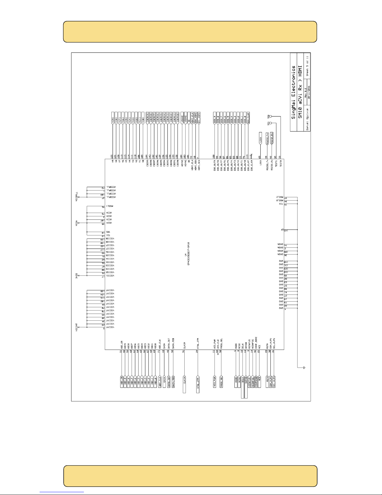
Figure 7 SB10 schematics - Sheet 5. ...................................................................................................... 14
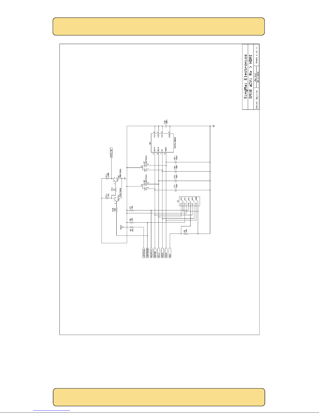
Figure 8 SB10 schematics - Sheet 6........................................................................................................15
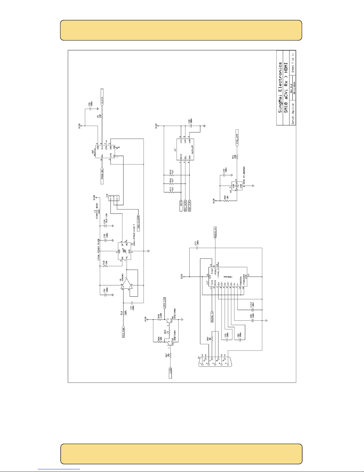
Figure 9 SB10 schematics - Sheet 7....................................................................................................... 16
Figure 10 SB10 schematics - Sheet 8. .....................................................................................................17
Figure 11 SB10 schematics - Sheet 9...................................................................................................... 18
Figure 12 SB10 schematics - Sheet 10. ................................................................................................... 19
Figure 13 SB10 schematics - Sheet 11.....................................................................................................20
Figure 14 Re-programming the SB10. ....................................................................................................21
Figure 15 Quartus FPGA programmer................................................................................................... 22
Figure 16 NTSC 75% colour bars - waveform......................................................................................... 23
Figure 17 NTSC 75% colour bars - vectors. .............................................................................................24
Figure 18 NTSC - SDI status display. ......................................................................................................24
Figure 19 PAL 75% colour bars - waveform. .......................................................................................... 25
Figure 20 PAL 75% colour bars - vectors................................................................................................ 25
Figure 21 PAL 75% colour bars - lightning. .............................................................................................26
Figure 22 PAL - CCIR17 waveform. ........................................................................................................26
Figure 23 PAL - 2T pulse......................................................................................................................... 27
Figure 24 PAL - 5.75MHz frequency sweep. ......................................................................................... 27
Figure 25 AC-DC adaptor specification- Page 1.....................................................................................28
Figure 26 AC-DC adaptor specification- Page 2. ...................................................................................29

SingMai Electronics
SB10 User Manual Revision 0.1 Page 4 of 29
1. Introduction
SB10 is a high quality NTSC/PAL video decoder module intended as a demonstration and evaluation
platform for the SingMai PT4 video decoder IP core.
The module accepts PAL or NTSC encoded CVBS (composite) inputs, either differential twisted pair
or single ended coaxial formats. The video is amplified, clamped and converted to digital video
using a 10-bit ADC clocked at 54MHz. An Altera FPGA is programmed with the PT4 video decoder,
which performs high quality line comb decoding of the video input. Both lock modes of the PT4
are supported –the voltage controlled oscillator (VCO) mode and the fast direct digital synthesis
(DDS) mode.
The BT656 output of the PT4 drives an HDMI transmitter allowing evaluation of the IP on a
monitor or waveform analyser. The HDMI output is set to 576i (PAL) or 480i (NTSC).

SingMai Electronics
SB10 User Manual Revision 0.1 Page 5 of 29
2. Connecting up the module
The SB10 module is powered by a universal input (90-260VAC) AC-DC adaptor, details of the
adaptor may be found in Appendix A. The 5VDC, 12W output of the supplied adaptor should be
connected to the jack input, ‘+5V IN’, of the SB10. Once connected, the green LED, ‘FPGA OK’
should light, indicating the FPGA has been correctly configured and the module is running. The
module is protected against over-voltage and reverse voltage inputs.
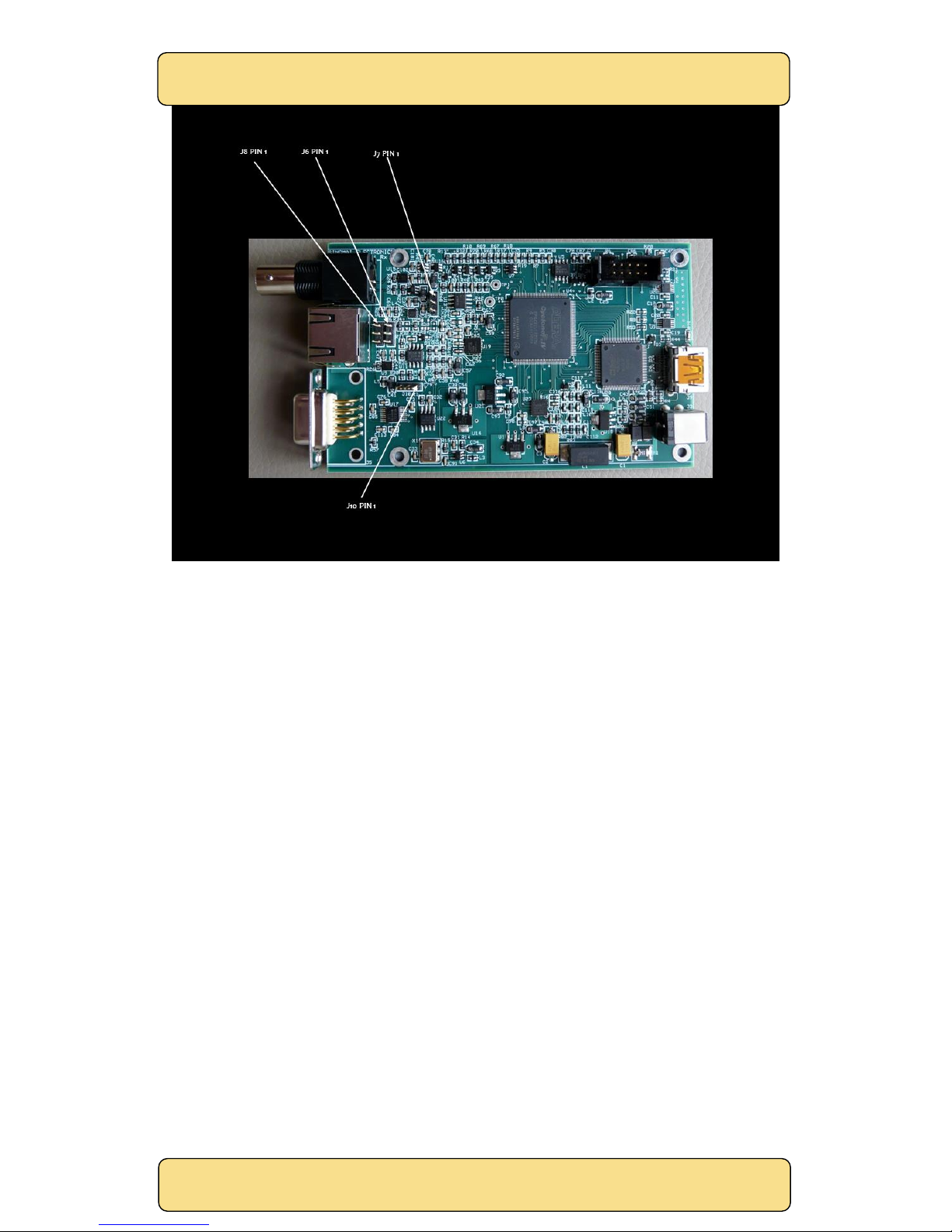
Figure 1 shows the SB10 interconnections.
Figure 1 SB10 Connectors.
SB10 accepts either NTSC-M or PAL inputs which it auto detects based on the measured line count.
To switch between the two cable types (twisted pair or coaxial) it is necessary to change some link
headers (see Figure 2) There are two 3-pin headers that select the video input source (J6) and a
voltage reference (J7). For coaxial inputs each connector should be linked pin 1 to pin 2; for UTP
cable pin 2 and pin 3 should be linked. Pull off the small pin header and place over the pins you
require for your cable type. Connector J8 should be left open for both cable types.
For UTP, twisted pair, cable the RJ-45 connector pins used are pin 1, video+ and pin 2 is video-. The
other pins are open.
For either cable type, if the input can be synchronized to (i.e. it is a valid video format) the ‘LOCK’
LED should light. Note it can take a few seconds for the input format to be determined and the
LED to light.
Finally, connect your HDMI receiver (e.g. monitor). If a HDMI source is detected the ‘HDMI HPD’
LED will light. It should now be possible to view the decoded video.
SingMai Electronics
SB10 User Manual Revision 0.1 Page 6 of 29
Figure 2 SB10 Jumper positions.
The PT4 decoder has two lock modes, and both are supported by the SB10 board. The first is to
use a voltage controlled oscillator. This mode is selected by linking pins 2 and 3 of the header, J10.
To select the DDS clock mode links pins 1 and 2 of J10. For a description of the two modes see the
Technical Description below, sheets 7 and 8.

SingMai Electronics
SB10 User Manual Revision 0.1 Page 7 of 29
3. Data Transfers
TBD.

SingMai Electronics
SB10 User Manual Revision 0.1 Page 8 of 29
4. Circuit description
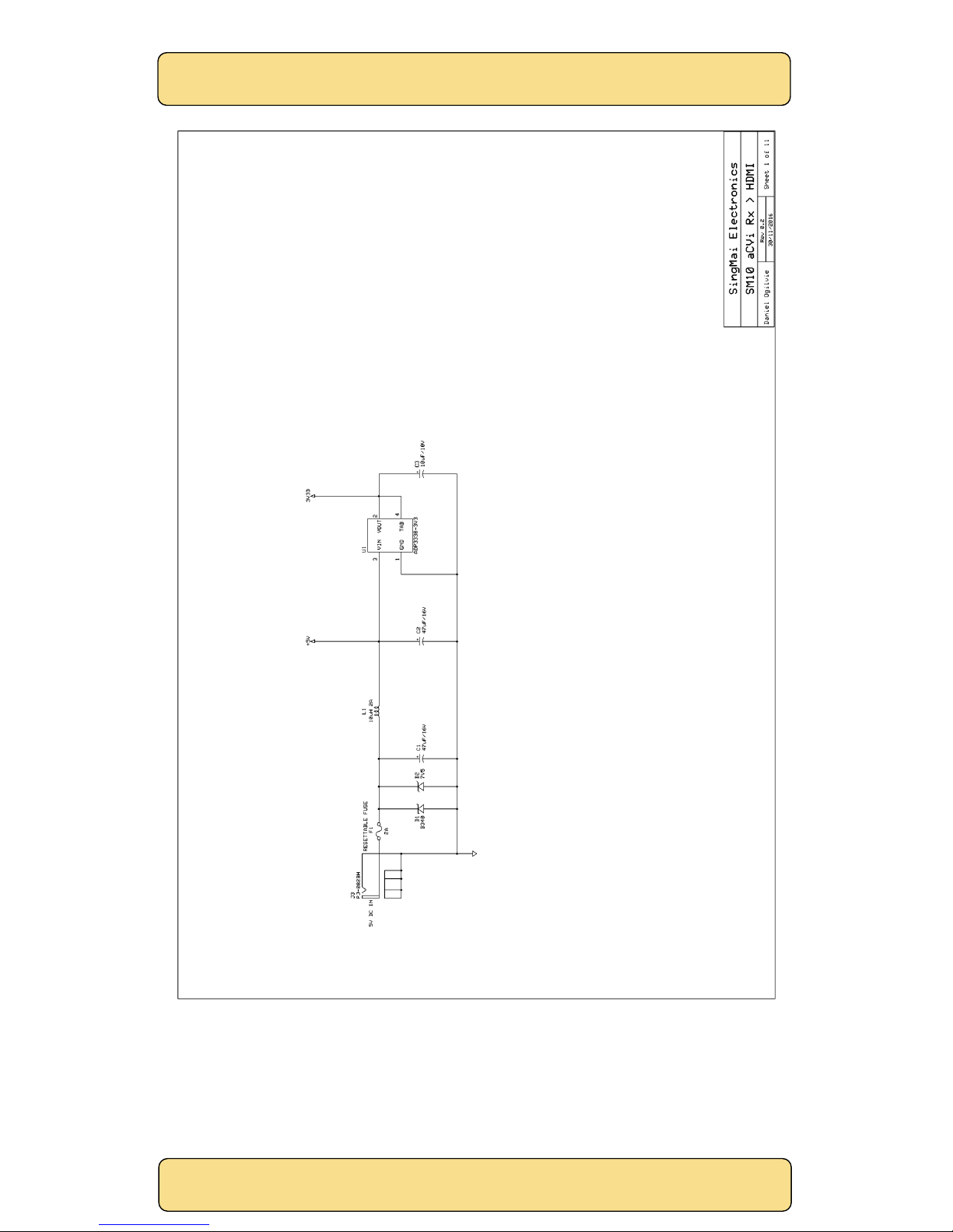
Figures 3-13 show the schematics for the SB10. Below is a brief technical description of the SB10
module.
Sheet 1.
J3 is the 5VDC power input connector to the SB10 module. The 5VDC is protected from over-
voltage and reverse polarity inputs by D1, D2 and resettable fuse, F1. The input is then filtered by L1
and C2 to provide the ‘clean’ 5VDC for the analogue input stage and also linear regulated by U1 to
provide the 3.3VDC supply voltage.
Sheet 2.
U2 provides the 1.2VDC for the internal voltage of the FPGA. U3 provides the 2.5VDC for the
analogue PLL circuity of the FPGA and L2 and C25 filter the VCCINT for the FPGA PLL digital blocks.
U18 provides the 1.8V supply to the HDMI transmitter.
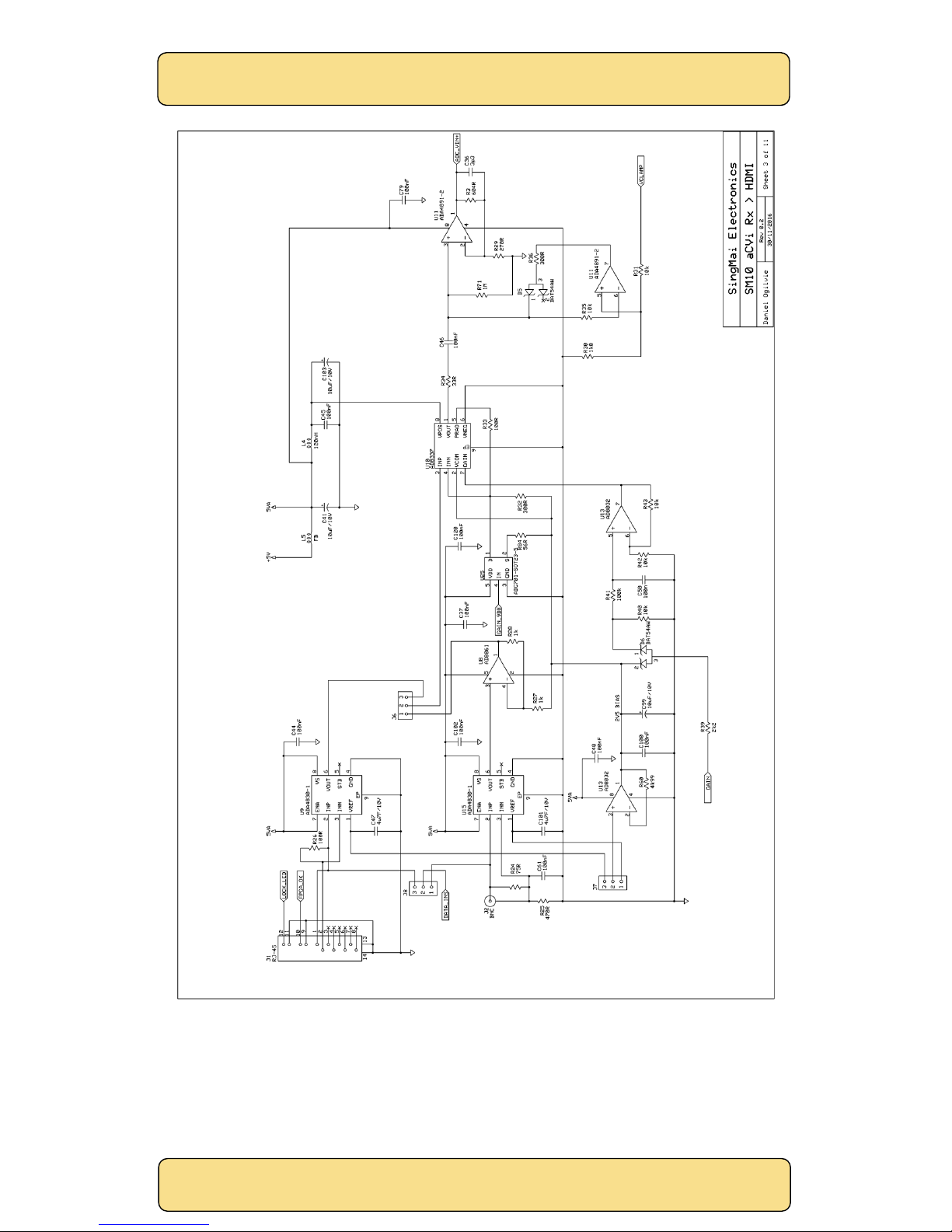
Sheet 3.
Sheet 3 is the analogue front end (AFE). The analogue video inputs, which may be NTSC or PAL,
may be either coaxial or twisted pair.
If twisted pair, they are terminated in 100Ω (R26) and converted from differential to single ended
outputs by U9. If coaxial inputs they are treated as a pseudo-differential input, with the ground
screen of the BNC input connector connected to ground via R25 and C61, which affords some hum
rejection for long cable runs. U15 converts this pseudo-differential input to a singled ended output
while U8 provides 6dB of gain to compensate for the attenuation in U15.
J6 selects either the differential or coaxial video input and J7 selects the mid-rail voltage offset
used by the AFE.
U10 is a voltage controlled amplifier. The PT4 decoder measures the amplitude of the
synchronizing signals and compares them to an internal reference: this amplifier compensates for
any loss in the input signal. U25 is not used in this application.
The output of U10 is AC coupled into U11A, which is a high input impedance, low input bias current
op-amp. The average DC level of video varies widely and to ensure it can be scaled into the
analogue to digital converter (ADC) properly it must be clamped. The AFE uses a sync tip clamp.
The most negative part of the AC coupled video is clamped to the VCLAMP reference voltage,
which is the most negative reference voltage of the ADC. The ADC requires a 0.5V to 2.5V (2V pk-
pk) input signal and the sync tips (the most negative part of the video signal) are clamped, using
‘ideal’ diode D5 and U11B, to the 0.5V ADC reference. The black level of the video (back porch
level) is measured and used to restore the video black level by the PT4 decoder.
Sheet 4.
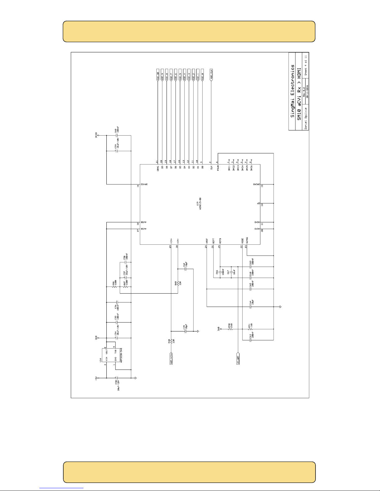
U19 is a 10 bit, 80MHz ADC which is run at 54MHz. The ADC is used in single-ended mode. The
clamped video from U11A is applied to the VIN+ input, and VIN- input is biased to mid rail (1.5V).
U14 provides the ‘clean’ 3.0V supply for the ADC. The output of the ADC, ADC[9:0] is the straight
binary coded, digital composite video which is applied directly to the PT4 decoder.
Sheet 5.
U4 is the FPGA. The FPGA is an Altera EP4CE15 device in a 144 pin 0.5mm TQFP package. The FPGA
contains the PT4 NTSC/PAL decoder and a SingMai PT13 control microprocessor which also
provides the I2C control to the HDMI transmitter.
Sheet 6.
The FPGA is a volatile device and needs configuring on switch on, which it does using U5, a 4Mb
EEPROM. The device is automatically configured on switch on, and successful configuration is
indicated by LED, ‘FPGA OK’. The EEPROM may also be reprogrammed via J4, which is compatible
with the Altera ‘USB-Blaster’ and the Quartus Programmer.

SingMai Electronics
SB10 User Manual Revision 0.1 Page 9 of 29
Sheet 7.
Two clock sources for the PT4 are available.
The PT4 decoder requires a line locked clock. The first option to achieve this is a voltage controlled
crystal oscillator, with the frequency of the oscillator controlled using a PWM output from the PT4
IP core. This output, VCO_PWM, is filtered by R14 and C31 to provide an analogue voltage which is
buffered by U6. The resulting 0-3.3V control voltage adjusts the frequency of the crystal voltage
controlled oscillator (VCXO), X1. The adjustment range is approximately ±150ppm. The centre
frequency (1.65VDC control voltage) is 27.0MHz.
The output of the VCXO is then multiplied to 74.25MHz or 74.18MHz (this is for backward
compatibility to HD video) –selection is performed via the FREQ_SEL port. For the PT4 the clock
input is 74.25MHz which is then divided down in the FPGA to provide the 27MHz and 54MHz clocks
required by the PT4. The other clock mode is described in Sheet 8.
The ‘LOCK’ LED is driven from a port of the FPGA. It is lit when the PT4 decoder status indicates
that horizontal lock has been achieved and the input is a valid standard supported by the decoder.
U7 is a proprietary copy-protection IC. U7 calculates a checksum from a PT13 generated data
stream, and the calculated checksum from U7 is compared with an FPGA internally generated
checksum. If the two do not match the SB10 module is shut down. This means that even if the bit
stream of the FPGA/EEPROM is captured the SB10 will not run without U7 being fitted.
U17 is an RS232 level translator. The RS232 data interface is described in Chapter 3.
X2 provides a fixed 27MHz clock. This provides a stable clock to the microcontroller and also for
the DDS 150MHz clock.
Sheet 8.
Sheet 8 provides an alternative to the crystal lock (see Sheet 7) with a wider lock range. The PT4
decoder generates a sinewave of approximate 27MHz frequency. The sinewave is converted to
analogue by U23 and then filtered to remove clock components. The zero crossing point of this
waveform is then detected by U24 which then provides a digital 27MHz clock. The frequency of
this sinewave is then adjusted by the PT4 decoder until horizontal lock is achieved.
Sheet 9.
Sheet 9 permits data to be inserted into ther video stream (from receiver to transmitter). This
feature is not supported in the PT4.
Sheet 10.
U20 is the HDMI transmitter. The PT4 provides BT656 formatted data which drives the HDMI
transmitter directly. Control of the transmitter is provided by the FPGA via an I2C interface.
Sheet 11.
J9 is the HDMI connector. D3, D4 and D9 provide overshoot protection for the TDMS signals. D10
indicates if an HDMI receiver has been detected (hot plug detect).
SingMai Electronics
SB10 User Manual Revision 0.1 Page 10 of 29
Figure 3 SB10 schematics - Sheet 1.

SingMai Electronics
SB10 User Manual Revision 0.1 Page 11 of 29
Figure 4 SB10 schematics - Sheet 2.
SingMai Electronics
SB10 User Manual Revision 0.1 Page 12 of 29
Figure 5 SB10 schematics - Sheet 3.
SingMai Electronics
SB10 User Manual Revision 0.1 Page 13 of 29
Figure 6 SB10 schematics - Sheet 4.
SingMai Electronics
SB10 User Manual Revision 0.1 Page 14 of 29
Figure 7 SB10 schematics - Sheet 5.
SingMai Electronics
SB10 User Manual Revision 0.1 Page 15 of 29
Figure 8 SB10 schematics - Sheet 6.
SingMai Electronics
SB10 User Manual Revision 0.1 Page 16 of 29
Figure 9 SB10 schematics - Sheet 7.

SingMai Electronics
SB10 User Manual Revision 0.1 Page 17 of 29
Figure 10 SB10 schematics - Sheet 8.

SingMai Electronics
SB10 User Manual Revision 0.1 Page 18 of 29
Figure 11 SB10 schematics - Sheet 9.

SingMai Electronics
SB10 User Manual Revision 0.1 Page 19 of 29
Figure 12 SB10 schematics - Sheet 10.

SingMai Electronics
SB10 User Manual Revision 0.1 Page 20 of 29
Figure 13 SB10 schematics - Sheet 11.
Table of contents
Other Singmai Electronics Media Converter manuals


