SIS SIS8300-KU User manual

Struck Documentation
SIS8300-KU
MTCA.4 Digitizer
Page 1 of 92
SIS8300-KU
10 channel
125 MSPS 16-bit
MTCA.4 Digitizer
User Manual
SIS GmbH
Harksheider Str. 102A
22399 Hamburg
Germany
Phone:
++49 (0) 40 60 87 305 0
Fax:
++49 (0) 40 60 87 305 20
http://www.struck.de
Version: SIS8300KU-M-x002-1-V101.doc as of 09.03.2017
Struck Documentation
SIS8300-KU
µTCA 16-bit Digitizer
Page 2 of 92
Revision Table:
Revision
Date
Modification
0.01
24.10.2016
Based on SIS8300L2-M-x00D-1-V110 (Firmware: V100D)
0.02
25.10.2016
Chapter "Functionality" updated
Chapter "Block diagram" updated
Chapter "Platform Management" MMC scheme updated
Chapter "MGT clock" scheme updated
Chapter "Frontpanel" sketch updated
Chapter 5.1 changed from Harlink to "RJ45 In-/Outputs" and updated
Chapter "Board Layout" print and used connector table updated
Chapter "Firmware Options register" updated
Chapter "RJ45 connector... register" updated
Chapter "SIS8900 RTM LVDS ... register" updated
Chapter "Ordering Options" updated
Chapter "Zone 3 connector schematic" updated
0.03
09.11.2016
Chapter "Functionality" updated
0.04
12.12.2016
Register description update
0.05
Block diagram update
0.06
15.12.2016
Chapter "Overall Clock distribution" updated
Chapter "Interlock" updated
Chapter "SIS8900 RTM LVDS ... register" updated
1.00
13.01.2017
First official release
Based on firmware sis8300KU_x001
1.01
09.03.2017
Release related to firmware sis8300KU_x002 (IP sis8300KU_x802 )
Added feature in firmware:
-FPGA Boot SPI Flash interface to update the FPGA Boot Flash via PCIe

Struck Documentation
SIS8300-KU
MTCA.4 Digitizer
Page 3 of 92
- Table of contents
-Table of contents............................................................................................................................................. 3
1Introduction..................................................................................................................................................... 5
1.1 Related documents .................................................................................................................................. 5
2Design............................................................................................................................................................. 6
2.1 Functionality ........................................................................................................................................... 6
2.2 Block Diagram........................................................................................................................................ 6
2.3 Platform Management............................................................................................................................. 7
2.3.1 E-Keying ......................................................................................................................................... 7
2.3.2 MMC sensors.................................................................................................................................. 8
2.3.3 MMC firmware upgrade.................................................................................................................. 8
2.4 SPI Connectivity ..................................................................................................................................... 9
2.5 JTAG Connectivity ............................................................................................................................... 10
2.6 ADC Temperature Sensors.................................................................................................................... 10
2.7 DAC...................................................................................................................................................... 11
2.8 Clock Distribution................................................................................................................................. 12
2.8.1 Overall Clock Distribution............................................................................................................ 12
2.8.2 DAC Clock.................................................................................................................................... 13
2.8.3 µRTM Clock Overview................................................................................................................. 13
2.8.4 TCLK Clock Overview................................................................................................................. 13
2.8.5 AMC_TCLK on Zone 3................................................................................................................ 14
2.8.6 MGT Clock ................................................................................................................................... 15
3Jumper/Connector Pin Assignments ............................................................................................................. 16
3.1 CON100 JTAG ..................................................................................................................................... 16
3.2 J604 Watchdog Reset............................................................................................................................ 16
3.3 J32 AVR JTAG..................................................................................................................................... 17
3.4 J33 ATxmega128 Debug....................................................................................................................... 17
4LEDs............................................................................................................................................................. 18
4.1 Module Management LEDs .................................................................................................................. 18
4.2 Front Panel LEDs.................................................................................................................................. 18
4.3 SMD LEDs............................................................................................................................................ 19
5Front panel .................................................................................................................................................... 20
5.1 RJ45 LVDS In-/Outputs........................................................................................................................ 21
5.2 SMA Clock Input................................................................................................................................. 22
5.3 SFP Card Cage...................................................................................................................................... 22
6Board Layout ................................................................................................................................................ 23
7Firmware Description ................................................................................................................................... 24
7.1 ADC Sample Logic............................................................................................................................... 24
7.2 Memory Interface.................................................................................................................................. 25
7.2.1 Memory Write Interface................................................................................................................ 26
7.3 Memory buffer ...................................................................................................................................... 27
7.4 Address Map ......................................................................................................................................... 28
7.5 Register description............................................................................................................................... 30
7.5.1 Module Id. and Firmware Revision register.................................................................................. 30
7.5.2 Serial Number register .................................................................................................................. 30
7.5.3 User Control/Status register ......................................................................................................... 31
7.5.4 Firmware Options register............................................................................................................. 32
7.5.5 ADC Temperature Sensor interface register ................................................................................. 33
7.5.6 Firmware Options register............................................................................................................. 34
7.5.7 ADC Acquisition Control/Status register..................................................................................... 35
7.5.8 ADC Sample Control register ....................................................................................................... 36
7.5.9 MLVDS Input/Output Control register ......................................................................................... 37
7.5.10 RJ45 Connector Input/Output Control register ............................................................................. 38
7.5.11 SFP1 Link Control/Status register................................................................................................. 39
7.5.12 SFP2 Link Control/Status register................................................................................................. 40
7.5.13 Port12 Link Control/Status register............................................................................................... 41
7.5.14 Port13/14/15 Link Control/Status register..................................................................................... 42

Struck Documentation
SIS8300-KU
µTCA 16-bit Digitizer
Page 4 of 92
7.5.15 DAC Trigger Control register ....................................................................................................... 43
Synch-Mode = 1: Both DACs are triggered synchronous with DAC1 “Start-logic” ................................... 43
7.5.16 Clock Distribution Multiplexer control register............................................................................ 44
7.5.17 Clock Distribution AD9510 Serial Interface (SPI) interface register............................................ 46
7.5.18 Clock Multiplier IC SI5326 SPI interface register....................................................................... 48
7.5.19 Clock Synthesizer IC Si5338A I²C interface register.................................................................... 49
7.5.20 FPGA Boot SPI Flash interface..................................................................................................... 50
7.5.21 DAC Control register .................................................................................................................... 51
7.5.22 DAC Data register......................................................................................................................... 52
7.5.23 RTM I2C interface register ........................................................................................................... 53
7.5.24 ADC Serial Interface (SPI) interface register................................................................................ 54
7.5.25 ADC Input Tap delay register ....................................................................................................... 55
7.5.26 DAC Trigger and DAC_CLK prescaler setup register.................................................................. 56
7.5.27 DAC RAM endpoint register ........................................................................................................ 57
7.5.28 Trigger registers ............................................................................................................................ 58
7.5.29 Memory Sample Start Block Address / Actual Sample Block Address registers.......................... 61
7.5.30 Sample Block Length register....................................................................................................... 62
7.5.31 Ringbuffer Delay register.............................................................................................................. 62
7.5.32 SIS8900 RTM LVDS Test Input/Output Control register............................................................. 63
7.5.33 Read DMA System Destination address (lower 32bits)................................................................ 65
7.5.34 Read DMA System Destination address (upper 32bits)................................................................ 65
7.5.35 Read DMA Card Memory Source address.................................................................................... 65
7.5.36 Read DMA Transfer length........................................................................................................... 66
7.5.37 Read DMA Control....................................................................................................................... 66
7.5.38 Readout DMA Sample byte swap ................................................................................................. 67
7.5.39 Write DMA System Source address (lower 32bits) ...................................................................... 68
7.5.40 Write DMA System Source address (upper 32bits) ...................................................................... 68
7.5.41 Write DMA Card Memory Destination address............................................................................ 68
7.5.42 Write DMA Transfer length.......................................................................................................... 69
7.5.43 Write DMA Control ...................................................................................................................... 69
7.5.44 Write DMA maximal number of Outstanding Requests ............................................................... 69
7.5.45 DAQ Done DMA Chain Control................................................................................................... 70
7.5.46 IRQ Enable.................................................................................................................................... 70
7.5.47 IRQ Status..................................................................................................................................... 71
7.5.48 IRQ Clear...................................................................................................................................... 71
7.5.49 IRQ Refresh .................................................................................................................................. 71
7.5.50 Memory test mode register............................................................................................................ 72
7.6 External register interface ..................................................................................................................... 73
7.7 User Blockram DMA Interface............................................................................................................. 75
7.8 User Interrupt Interface......................................................................................................................... 76
8µRTM management ...................................................................................................................................... 77
9FPGA Firmware upgrade.............................................................................................................................. 78
9.1 JTAG Firmware Upgrade procedure..................................................................................................... 78
9.1.1 Use of Xilinx Vivado Hardware Manager..................................................................................... 78
9.2 Linux tool ‘flashupdater’....................................................................................................................... 80
9.3 Linux tool ‘ipmitool’............................................................................................................................. 80
9.4 Linux workaround for PCIe-Hot-Plug .................................................................................................. 81
10 Appendix................................................................................................................................................... 82
10.1 Power Consumption.............................................................................................................................. 82
10.2 Ordering options.................................................................................................................................... 82
10.3 SFP+ Accessories.................................................................................................................................. 82
10.4 Zone 3 connectors J30 and J31 ............................................................................................................. 83
10.4.1 J31 connector pin assignments...................................................................................................... 83
10.4.2 J30 connector pin assignments...................................................................................................... 83
10.5 Note on AC/DC input stage selection ................................................................................................... 85
10.5.1 Interlock ........................................................................................................................................ 87
10.6 Zone 3 connector schematic.................................................................................................................. 88
10.7 MMC Readme file................................................................................................................................. 89
11 Index ......................................................................................................................................................... 90
Struck Documentation
SIS8300-KU
MTCA.4 Digitizer
Page 5 of 92
1 Introduction
The SIS8300-KU is a 10 channel 125 MS/s digitizer with 16-bit resolution according to the
MTCA.4 standard.
SIS8300-KU
Note: While the SIS8300-KU is Kintex Ultrascale based you will find many Virtex 5/6 references in
the firm- and software for historical reasons (i.e. remnants from the SIS8300_V2 and SIS8300L2
designs).
As we are aware, that no manual is perfect, we appreciate your feedback and will incorporate proposed
changes and corrections as quickly as possible. The most recent version of this manual can be obtained
from our Dokuwiki at www.struck.de/dokuwiki. Please direct account requests to info@struck.de.
1.1 Related documents
A list of available firmware designs can be retrieved from http://www.struck.de/SIS8300firm.html
Struck Documentation
SIS8300-KU
MTCA.4 Digitizer
Page 6 of 92
2 Design
The central building block of the SIS8300-KU card is a Xilinx Kintex Ultrascale FPGA. It holds the 4
lane PCI Express interface and is in control of all active components.
2.1 Functionality
The key properties of the SIS8300-KU card are listed below.
AMC .4 µTCA for Physics Board
4 Lane PCI Express Gen3 Interface
Dual zSFP+ Card Cage for optional Multi Gigabit Link
Xilinx Kintex Ultrascale FPGA
DDR4 Memory Interface
4 x 4Gbit default DDR4 memory size
ATxmega128A1U Microcontroller IPMI
External Clock and Trigger Inputs
Front panel digital I/O (4in/4 out) on RJ45 Connectors
µRTM ADC Analog Inputs, I²C-Bus, DAC Analog Outputs
10 ADC Channels 125MS/s, 16-Bit
2 DAC Channels 250MS/s, 16-Bit
Clock distribution with phase shifting
4 M-LVDS µTCA Ports
2 µTCA Clocks
White Rabbit Option (depends on assembly)
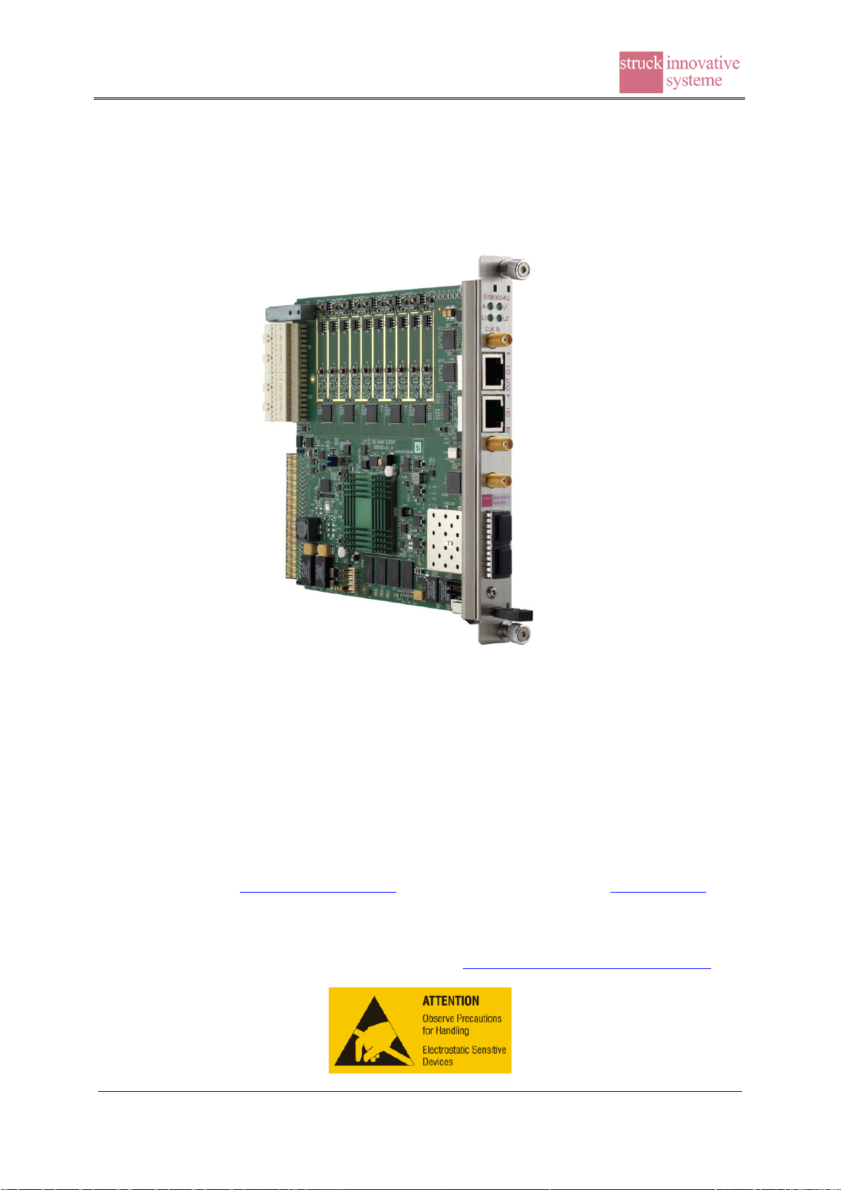
2.2 Block Diagram
A simplified block diagram of the SIS8300-KU is shown below.
SFP+
2 Ch DAC Out
Digital I/O
Kintex
Ultrascale
FPGA
SERPROM IPMI
SFP+
Ext Clock,
SMA
Dual
ADC
Ext Clock, Trigger,
LVDS
DDR4 Memory
IS
Clock
Distribution
IS
IS
Dual
ADC
Dual
ADC
Dual
ADC
Dual
ADC
IS
IS
IS
IS
IS
IS IS
LEDs/Switch SERPROM
BS

Struck Documentation
SIS8300-KU
MTCA.4 Digitizer
Page 7 of 92
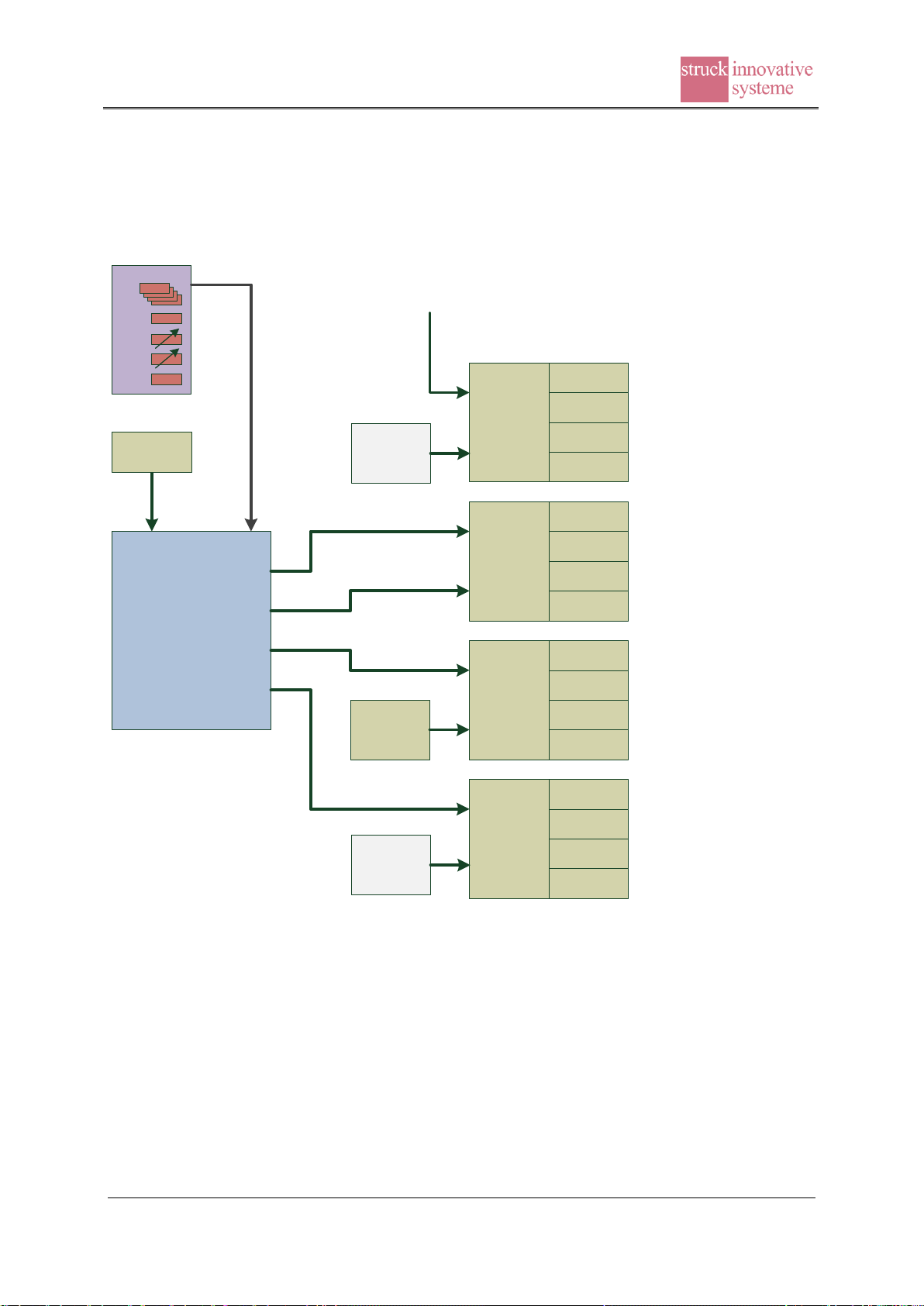
2.3 Platform Management
The Module Management Controller (MMC) functionality of the SIS8300-KU is implemented in an
Atmel ATxmega128A1U-CU microcontroller. The management code is based on the DESY MMC
V1.00 management software solution(*). It can be upgraded in two different ways (please refer to
section 2.3.3).
(*) The DESY Module Management Controller (MMC) software is licensed to Struck Innovative
Systeme GmbH under DESY LV92. Please, refer to the readme file in the appendix of this manual
also.
The MMC scheme of the SIS8300-KU is illustrated below.
Zone 3 ConnectorAMC Connector
FPGA
I2C Isolation
Control
SIS8300-KU
+3.3V / +12V
Power
Supplies
MMC
ATxmega128
FRU EEPROM
JTAG
Front
Panel
Temp.
Sensors Unique
ID Serial
Port
Power
Switch
I2C
Isolator
Driver
x
Power Control
and Monitoring
Management Bus
Isolation Control
Hot-plug and Status
Local I2C Bus
Debug
Management Bus
Presence Detect
Geographic Address
TCLK / ILOCK
Isolation Control
Power Control
and Status
JTAG
Isolator
Optional
AMC_TCLK
ILOCK
JTAG Isolation
Control
FPGA
User IO
Bus
Presence Detect
2x
EEPROM
FPGA Configuration
Upload
FPGA Config
Select
RTM I2C Bus
FPGA
User IO
FPGA
User IO
2.3.1 E-Keying
An Electronic Keying mechanism is used to provide correct connection and setup of point-to-point
fabrics and clocks for AMC modules in example. E-Keying information of the SIS8300-KU is stored
in the MMC as FRU information. It will be communicated to the MCH at power up. E-Keying entries
in the FRU information of the SIS8300-KU match the FPGA design at shipment version and are fixed.
If you change the FPGA design and/or make a custom FPGA design it can be necessary to change part
of the FRU information also.
The use of incorrect FRU information can result in unexpected behaviour.
Please contact us in case you need detailed information on SIS8300-KU E-Keying.
More information on this issue is planned for future additions to the documentation.
Struck Documentation
SIS8300-KU
MTCA.4 Digitizer
Page 8 of 92
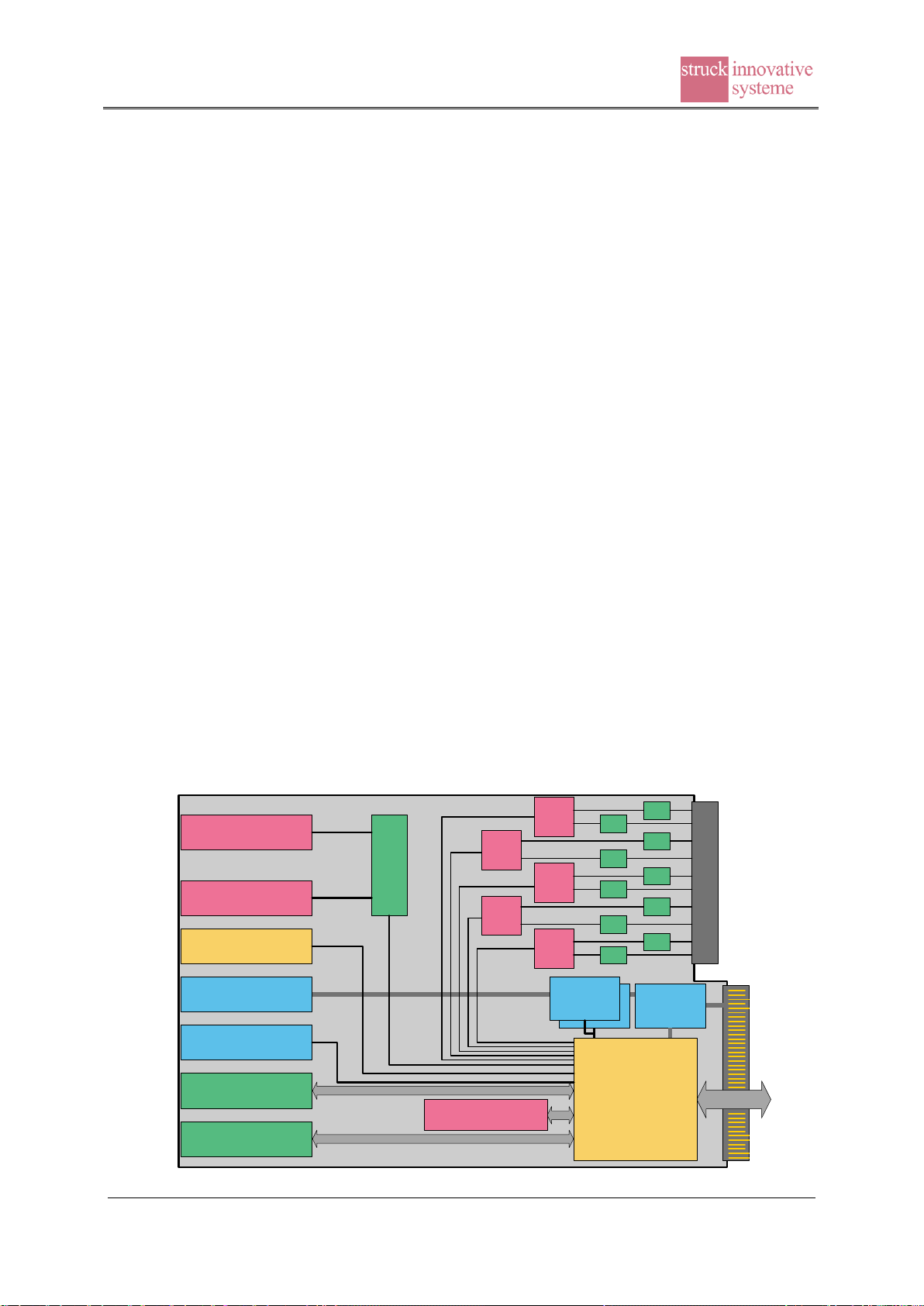
2.3.2 MMC sensors
Different sensors are connected to the MMC. They are giving information about temperatures,
voltages, currents and states. An additional memory with unique ID is available for board
identification purposes.
An overview of all existing SIS8300-KU MMC sensors –as seen with NATView- is illustrated below.
Note: On SIS8300-KU further temperature sensors exist, please see section 2.6.
2.3.3 MMC firmware upgrade
The MMC firmware can be upgraded in field over connector J32 or can be uploaded via
IPMI.
To upgrade in field you need an AVR programming tool, i.e. AVR JTAGICE mkII. After
connecting to connector J32 (please refer to section 3.3) the MMC can be upgraded using
Atmel-Studio software.
The more comfortable means for an upgrade is the upload of the MMC code over IPMI.
This can be done with the LINUX software ipmitool.
Syntax:
ipmitool -I lan -H <IP-MCH> -P "" -B 0 -b 7 -T 0x82 -t <Slot>
hpm upgrade SIS8300KU_VersionID.hpm
Slot: 0x72 (1st slot), 0x74 (2nd slot), 0x76 (3rd slot), ...
for example:
ipmitool -H 192.168.115.62 -P "" -B 0 -b 7 -T 0x82 -t 0x74 hpm upgrade SIS8300KU_VersionID.hpm
ipmitool -H 192.168.115.62 -P "" -B 0 -b 7 -T 0x82 -t 0x74 mc info
To verify, that the MMC was upgraded successfully, mc info can be read to check the MMC
code version.
Struck Documentation
SIS8300-KU
MTCA.4 Digitizer
Page 9 of 92
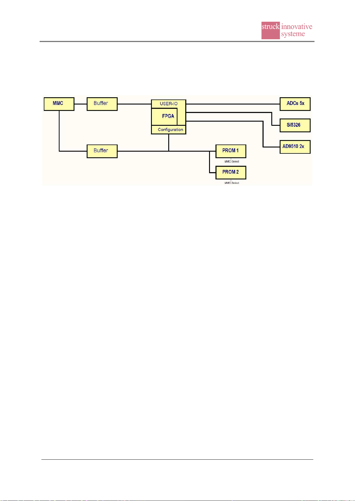
2.4 SPI Connectivity
The SPI bus connectivity scheme of the SIS8300-KU is illustrated below.
The SIS8300-KU has two SPI EEPROMs, that can hold FPGA configuration data. So it is
possible to choose from two firmware designs for the configuration of the FPGA. The
selection of the SPI EEPROM is under control of the MMC and can be changed per IPMI
command.
The ipmitool command line to set one of the Flashes as boot file source looks like:
ipmitool -I lan -H <IP-MCH> -P "" -B 0 -b 7 -T 0x82 -t <Slot>
raw 0x30 0x01 <Flash>
Flash: 0x00 (Basic-FLASH), 0x01 (Second-FLASH)
Slot: 0x72 (1st slot), 0x74 (2nd slot), 0x76 (3rd slot), ...
Verification:
ipmitool -I lan -H <IP-MCH> -P "" -B 0 -b 7 -T 0x82 -t <Slot>
raw 0x30 0x00
Result:
00 : Basic-FLASH selected
01 : Second-FLASH selected
IPMI raw command to reset the FPGA:
ipmitool -I lan -H <IP-MCH> -P "" -B 0 -b 7 -T 0x82 -t <Slot>
raw 0x30 0xFF
The user has to take special care to avoid concurrent access to the SPI EEPROM from
different sides (via PCIe and IPMI).
The SPI EEPROMs can be flashed via a JTAG-Programmer, PCIe or IPMI with appropriate
tools. Please refer to section 9 for more information about flashing the SPI EEPROM.
Struck Documentation
SIS8300-KU
MTCA.4 Digitizer
Page 10 of 92
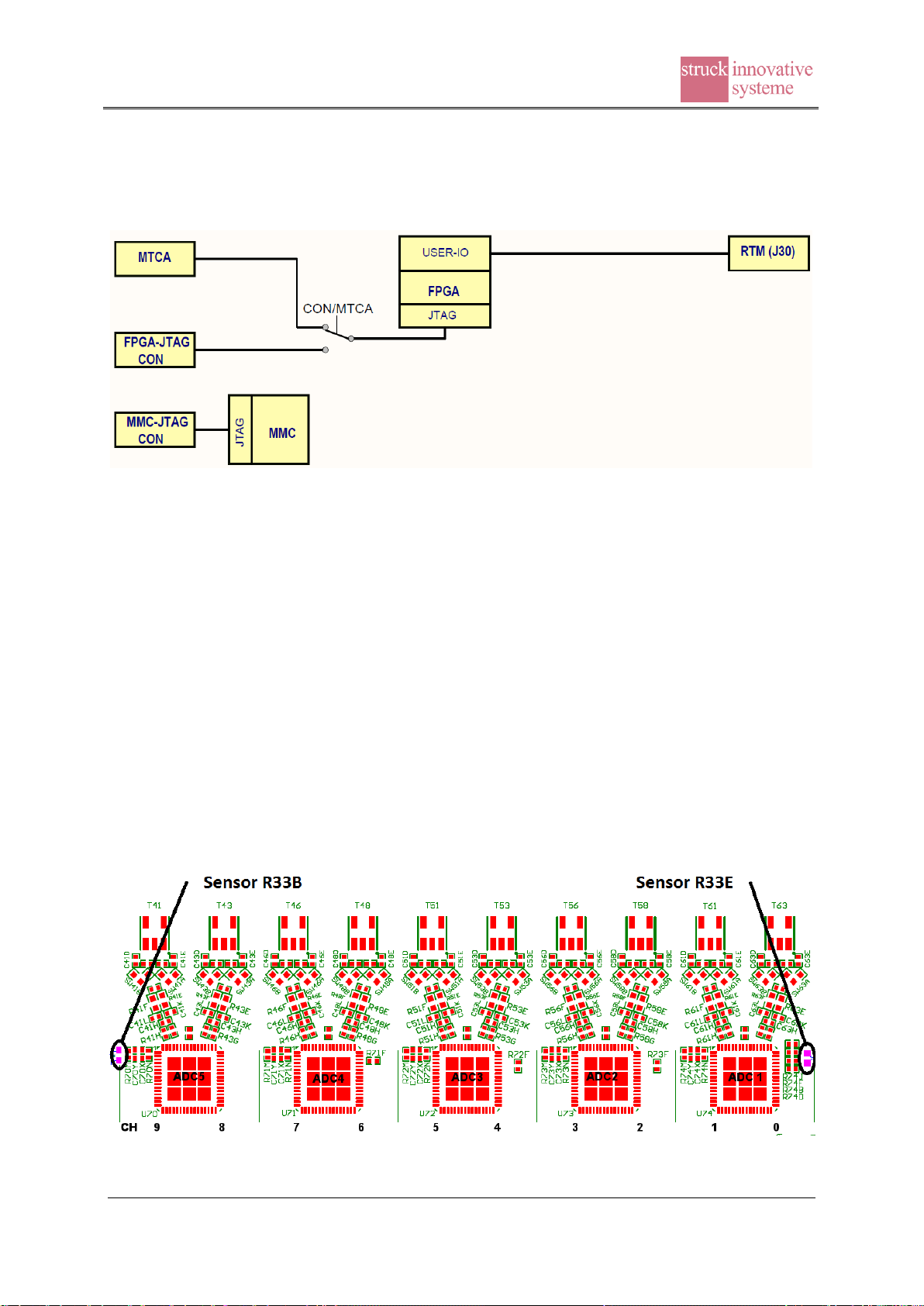
2.5 JTAG Connectivity
The JTAG connectivity scheme of the SIS8300-KU is illustrated below.
JTAG connection to µRTM can be realized in FPGA firmware but is a optional feature for
future.
Switching connection of FPGA hardware JTAG port between MTCA (AMC Backplane) and
on board JTAG connector (illustrated switch CON/MTCA) can be made via IPMI command.
IPMI command ... (not implemented yet, please request us for more information)
Upon power up the switch CON/MTCA connects the JTAG connector to the JTAG port of
the FPGA hardware.
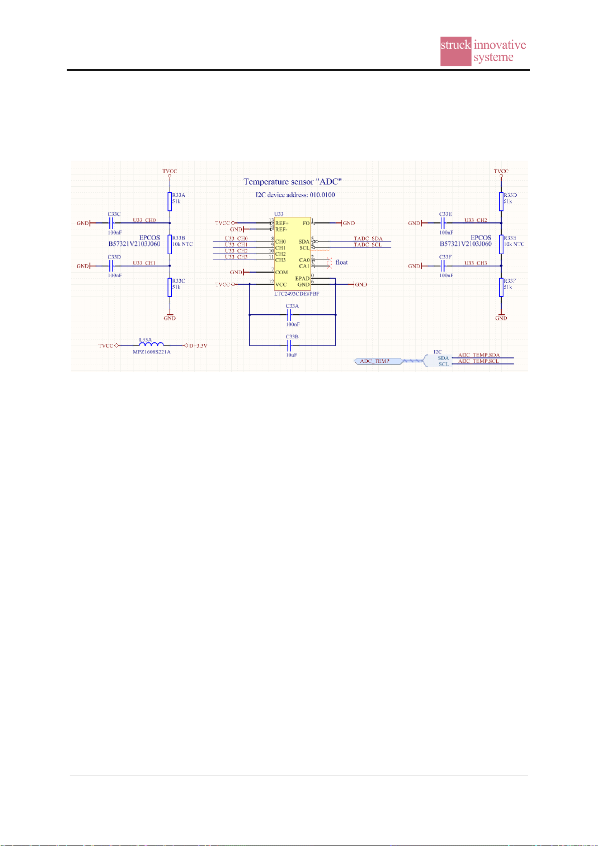
2.6 ADC Temperature Sensors
Two thermistor based sensors are used to measure the temperature at the beginning and the
end of the row of the 5 digitizer chips.
The location of both sensors on the bottom side as seen from the top is shown below.
Struck Documentation
SIS8300-KU
MTCA.4 Digitizer
Page 11 of 92
The sensor signals are measured by the 24-bit ΣΔ-ADC LTC2493, which is connected to the
Kintex Ultrascale FPGA via an I²C interface.
The schematic of the ADC temperature sensor circuitry is illustrated below.
Note: please refer to section 7.5.5 for a description of the I²C interface register
Please refer to device datasheet for additional information on the LTC2493 chip.
A software example can be found on the Struck product DVD under:
sisdvd_xxxxxx\sis8xxx and DWC\sis8300L\software\tests\adc_temp
2.7 DAC
A part of the SIS8300-KU versions comes with the 250 MSPS MAX5878 dual DAC chip.
The dual DAC can be used to control the Vectormodulator on the DWC8VM1
Downconverter/Vectormodulator RTM over the Zone 3 connector for example. The two DAC
channels can be routed to two front panel SMA outputs also (stuffing option). The table in
section 10.2 (ordering options) lists a number of DAC configurations of the SIS8300-KU.
Modules configured as DAC to FP outputs route the two DAC outputs over signal
conditioning stages to the two front panel SMA connectors. The default range of the DAC
outputs over the SMA connectors is -1V,…,+1V into a 50 Ω load.
On modules configured with DAC to Z3, the outputs of the DAC are directly connected to the
Zone 3 connector without any additional components. Since each DAC channel outputs two
complementary currents, appropriate signal conditioning has to be done on the µRTM.
Refer to the datasheet of the MAX5878 for further information.
Struck Documentation
SIS8300-KU
MTCA.4 Digitizer
Page 12 of 92
2.8 Clock Distribution
2.8.1 Overall Clock Distribution
The clock distribution scheme of the SIS8300-KU is illustrated below.
ADC
ADC
ADC
ADC
ADC
ADC
ADC
ADC
ADC
ADC
ΔT
ΔT
AD9510
ΔT
ΔT
AD9510
FPGA
CLK05
Ch0
Ch1
Ch9
RTM_CLK1
RTM_CLK0
ADCLK925
µRTM
RTM_CLK2
ADCLK944
EXTCLKA
SMA
TCLKB
Backplane
MUX BMUX A
ADCLK925 ADCLK946 ADCLK946
Quartz
ADCLK925ADCLK925
MUX D MUX E
MUX C
SI5326
EXTCLKB
RJ45
TCLKA
3
2
0
1
1
3
2
0
3
2
0
1
3 1 2 0 3 1 2 0
#1
#2 FPGA
CLK69
AMC_TCLK
ADCLK944
Quartz
(optional)
RTM_CLK4
RTM_CLK5
to FPGADAC Clock
DS25CP152
select
enable
under MMC Control
7
6
5
4
4
5
6
1
2
1
2
RJ45
CLK
7
1
1
2
Inputs:
MUX D àAD9510-#2_CLK1
RTM_CLK1 àAD9510-#2_CLK2
MUX E àAD9510-#1_CLK1
RTM_CLK0 àAD9510-#1_CLK2
Outputs:
AD9510-#2_OUT7 àFP_RJ45_E
AD9510-#2_OUT6 àADC4_CLK
AD9510-#2_OUT5 àADC5_CLK
AD9510-#2_OUT4 àFPGA_CLK69
AD9510-#2_OUT3 àN/A
AD9510-#2_OUT2 àN/A
AD9510-#2_OUT1 àFPGA_MGT_CLK
AD9510-#2_OUT0 àDIV1_OUT0 (DAC_MUX)
AD9510-#1_OUT7 àADC1_CLK
AD9510-#1_OUT6 àADC2_CLK
AD9510-#1_OUT5 àADC3_CLK
AD9510-#1_OUT4 àFPGA_CLK05
AD9510-#1_OUT3 àN/A
AD9510-#1_OUT2 àN/A
AD9510-#1_OUT1 àN/A
AD9510-#1_OUT0 àDIV0_OUT0 (DAC_MUX)
Depending from ordering options a 114.285 MHz clock will be populated. This external
reference is required for the SI5326 to perform jitter attenuation. Please refer to the SI5326
datasheet and section 10.2.

Struck Documentation
SIS8300-KU
MTCA.4 Digitizer
Page 13 of 92
2.8.2 DAC Clock
The DAC clock scheme of the SIS8300-KU is illustrated below.
FPGA DAC
DAC MUX
BUFFER
0
1
ΔT
ΔT
AD9510
#1
#2
ΔT
ΔT
AD9510
2
µRTM
3
RTM_CLK4
DIV0_OUT0
DIV1_OUT0
FPGA_FB
FPGA_CLK
DAC_CLK
16 DATA
DAC_SELIQ
0
0
2.8.3 µRTM Clock Overview
The µRTM clock overview table is shown below.
Clock
Usage
RTM_CLK0
Ultra low jitter clock 1 ADC group 1
RTM_CLK1
Ultra low jitter clock 2 ADC group 2
RTM_CLK2
Clock switch yard
RTM_CLK3
Not used
RTM_CLK4
DAC Clock
RTM_CLK5
Connected to FPGA via clock buffer
2.8.4 TCLK Clock Overview
An overview on the TCLK clocks is shown in the table below.
Clock
Usage
TCLKA
MUX switch yard and Zone 3 AMC_TCLK
TCLKB
MUX switch yard and Zone 3 AMC_TCLK
TCLKC
Not used, can be 100 Ω terminated if needed
TCLKD
Not used, can be 100 Ω terminated if needed

Struck Documentation
SIS8300-KU
MTCA.4 Digitizer
Page 14 of 92
2.8.5 AMC_TCLK on Zone 3
The AMC_TCLK signal can be derived from TCLKA or TCLKB. Selection and output
control of AMC_TCLK switch is under control of MMC. Currently the state of both signals
can be read from SIS8900 RTM LVDS Test Input/Output Control register, please refer to
section 7.5.32.
The TCLKA or TCLKB selection and switch output control can be made per IPMI command:
<IPMI> raw 0x30 0x03 0xEC
(E=1/0: TCLK active/deactivated, C=0/1: select TCLKA/TCLKB)
The status can be read back with the command:
<IPMI> raw 0x30 0x02
After power up TCLKA is selected per default.
AMC_TCLK signal is available for SIS8300-KU with Zone 3 class compatibility A1.1CO
and A1.0C only. Please refer to section 10.4.2.
Struck Documentation
SIS8300-KU
MTCA.4 Digitizer
Page 15 of 92
2.8.6 MGT Clock
The MGT (Multi Gigabit Transceiver) clock scheme of the SIS8300-KU is illustrated below.
PCIe 1 (Port 5)
PCIe 0 (Port 4)
SFP (L2)
SFP (L1)
clock from AMC Backplane
(FCLKA)
LLL (user links, Port 14)
LLL (Port 13)
LLL (Port 12)
Gbe (Port 0)
Gbe (Port 1)
SI5338A
Programmable
Quad Output
PLL
controlled via I2C
from FPGA
125 MHz
25 MHz
quartz
PCIe 3 (Port 7)
PCIe 2 (Port 6)
MGT
REFCLK0
LLL (low latency link, Port 15)
MGT
REFCLK1
MGT
REFCLK0
MGT
REFCLK1
MGT
REFCLK0
MGT
REFCLK1
MGT
REFCLK0
MGT
REFCLK1
227-2
227-3
227-0
227-1
226-2
226-3
226-0
226-1
225-2
225-3
225-0
225-1
224-2
224-3
224-0
224-1
IN1-2 IN5-6
C0
C1
C2
C3
ΔT
ΔT
AD9510
#2
DIV1_OUT1
oscillator
100 MHz
oscillator
(assembly option)
x MHz
WR - PLL
(assembly option)

Struck Documentation
SIS8300-KU
MTCA.4 Digitizer
Page 16 of 92
3 Jumper/Connector Pin Assignments
The following subsections describe jumper and connector pin assignments.
3.1 CON100 JTAG
The SIS8300-KU’s on board logic can load its firmware from two SPI EEPROMs (Basic
FLASH and Second FLASH), via the JTAG port on connector CON100, PCI Express, MTCA
or via the MMC.
Hardware like the XILINX HW-USB-JTAG in connection with the appropriate software will
be required for in field JTAG firmware upgrades.
CON100 is a 2mm (i.e. metric) 14 pin header that allows you to reprogram the firmware of
the SIS8300-KU board with a JTAG programmer. The pin out is shown in the schematic
below. It is compatible with the cable that comes with the XILINX HW-USB-II-G-JTAG
platform cable. CON100 can be found at the right bottom side of the board.
Note: The board has to be powered for reprogramming over JTAG
3.2 J604 Watchdog Reset
J604 can be found next to the left upper edge of U500 (largest chip on the card with green
heat sink). With J604 closed the boards watchdog reset is connected to the reset logic. J604
should be opened for JTAG firmware programming.
Struck Documentation
SIS8300-KU
MTCA.4 Digitizer
Page 17 of 92
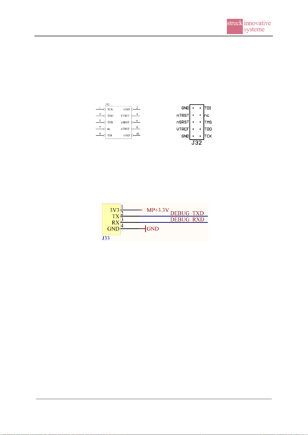
3.3 J32 AVR JTAG
This 10-pin header is used to connect to the JTAG of the Atmel ATxmega128 microcontroller
providing the IPMI/MCH functionality of the SIS8300-KU. J32 can be found at the left
bottom side of the board. The pin out is shown in the schematic below.
3.4 J33 ATxmega128 Debug
This 4 pin socket strip grants access to the debug port (PE2 and PE3) of the ATxmega128
microcontroller. It was designed in to facilitate Struck in house microcontroller software
development.
Note: Due to a lack of coding there is no protection against a wrong polarity connection. This
connector is reserved for Struck in house purposes only.

Struck Documentation
SIS8300-KU
MTCA.4 Digitizer
Page 18 of 92
4 LEDs
4.1 Module Management LEDs
Three right angle front panel LEDs (blue, red, green, not labelled) show the hot-swap status
and general module information about failures and out of service status.
The front panel Hot Swap handle has to be used for module insertion and extraction.
To insert the card, the Hot Swap handle must be pulled. The Hot Swap handle can pushed in
once the module is properly seated in the carrier backplane connector to initiate the MCH to
bring the module into operational state.
Typical module insertion process (module handle pushed in)
blue
red
green
Status
On
Off
Off
Module management controller start, activation process begins
Blink
Off
Off
Module activation process in progress, wait for payload power
Blink
On
Off
Payload power present, MMC waits for onboard Power Good
Off
Off
On
Power Good, FPGA loaded (done signal), module operational
Typical module extraction process (module handle pulled out)
blue
red
green
Status
Blink
Off
On
Module still operational, deactivation process begins, wait ...
Blink
On
Off
Payload power off, Module deactivation process in progress
On
Off
Off
Module deactivation finished and safe for extraction
Note: do not remove module before Hot Swap handle is pulled and the blue LED is solid on
4.2 Front Panel LEDs
The SIS8300-KU has additional 4 circular green front panel LEDs and 4 right angled green
LEDs next to dual SFP card cage. The function of the LEDs are shown in the table below.
LED name
Function in base design
A
PCI Express Access
U
User LED
L1
PCIe Link up
L2
ADC Sampling active
R (L1)
SFP Link 1 receiver loss of signal
T (L1)
SFP Link 1 transmitter fault
R (L2)
SFP Link 2 receiver loss of signal
T (L2)
SFP Link 2 transmitter fault
Note: if SIS8300-KU is in operational state and no SFP modules are present in SFP card cage
associated LEDs (R and T) are lit permanently

Struck Documentation
SIS8300-KU
MTCA.4 Digitizer
Page 19 of 92
4.3 SMD LEDs
A number of surface mount red LEDs are on the SIS8300-KU to visualize part of the board
status.
LED designator
LED comment
Function
D20A
S1
Firmware dependent
(Optical Link 1 up)
D20B
S2
Firmware dependent
(Optical Link 2 up)
D20C
S3
Firmware dependent
D20D
S4
Firmware dependent
D20E
S5
Firmware dependent
D20F
S6
Firmware dependent
D20G
S7
Firmware dependent
D20H
S8
Firmware dependent
D21D
READY
FPGA ready
D10A
+12V
Payload power present
D10B
MP+3.3V
Management power present

Struck Documentation
SIS8300-KU
MTCA.4 Digitizer
Page 20 of 92
5 Front panel
A sketch of the SIS8300-KU front panel view (with front panel I/O option) is shown below.
Table of contents
Other SIS Measuring Instrument manuals

Popular Measuring Instrument manuals by other brands


Trotec
Trotec BM12 operating manual

Endress+Hauser
Endress+Hauser TopClean S CPC 30 operating instructions

Max Machinery
Max Machinery 234 Series instruction manual

Rotronic
Rotronic HygroPalm Series instruction manual

Thermo Scientific
Thermo Scientific Eutech TN-100 Operation instructions

Burkert
Burkert SE30 Ex Namur operating instructions