– 6 – – 7 –
– 5 –
SECTION 3
CIRCUIT ADJUSTMENTS
SECTION 2
DISASSEMBLY
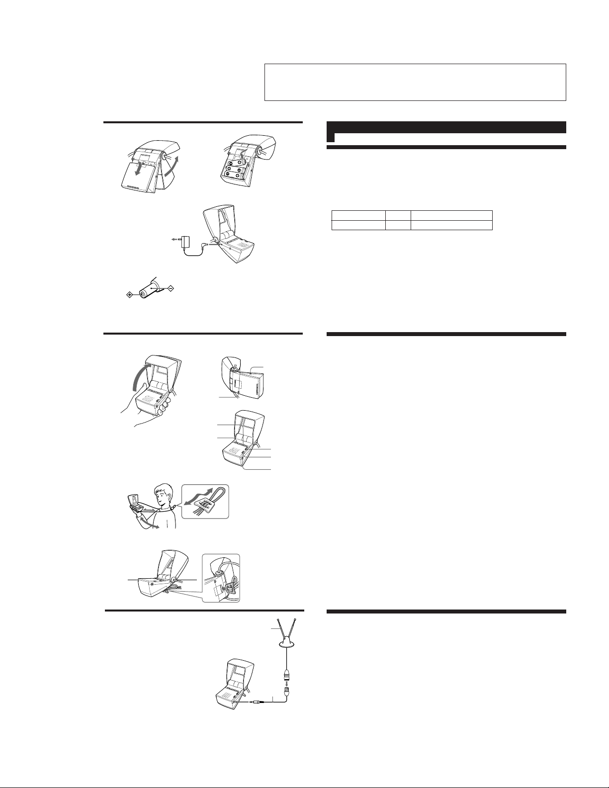
2-1. CASE, A BOARD AND H BOARD REMOVAL 2-2. LCD CASE AND B BOARD REMOVAL
2-3. SERVICE POSITION
2Three screws
(7-685-105-19)
3A board
4H board
1Battery cover
5Battery case (upper)
1Hinge collar
2LCD case (upper)
3LCD holder
4B board
Battery case (lower)
LCD case (lower)
Antenna
B board
Cord
AC power adaptor CN301
CN401
CN201
J101
J601
A board
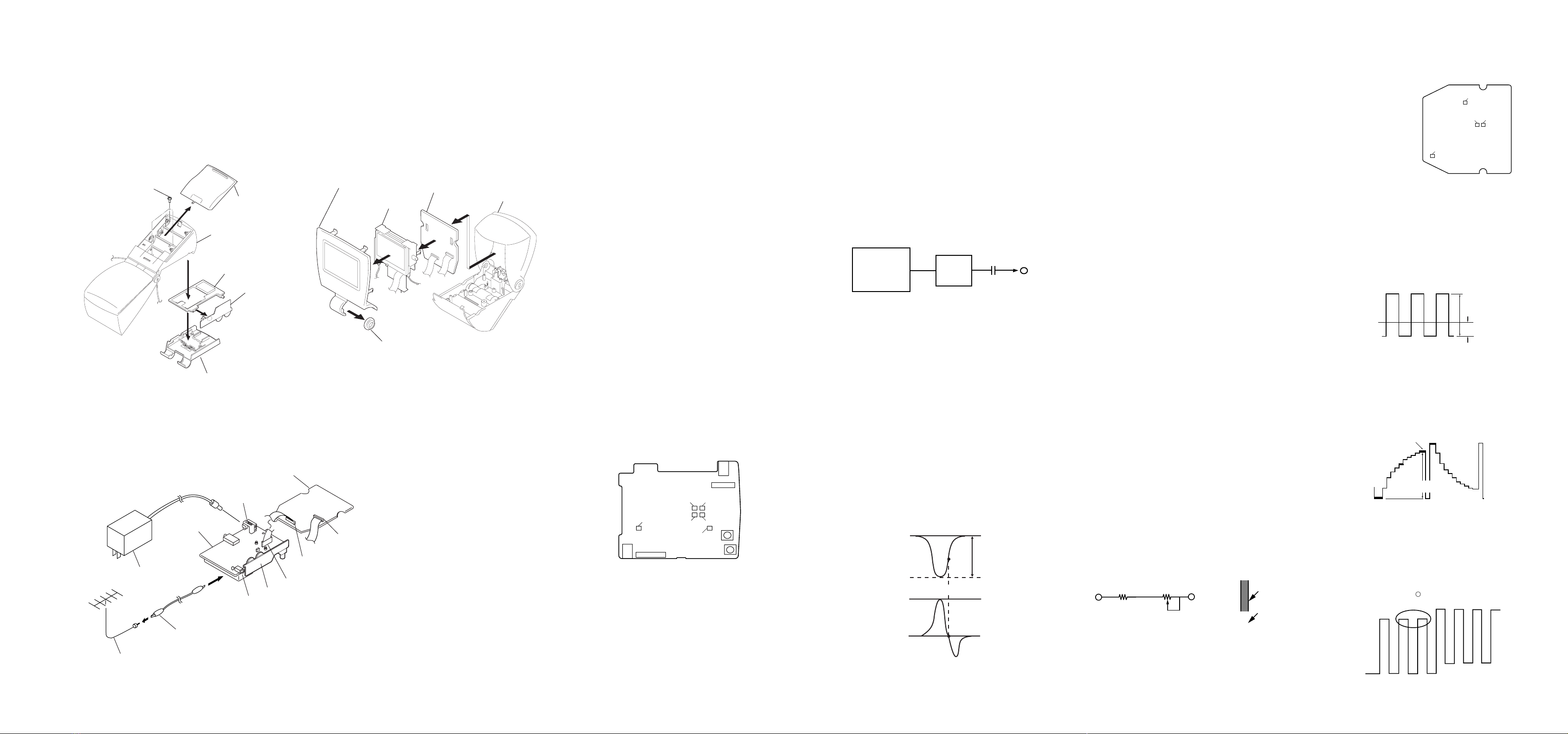
[SETUP](A BOARD )
1. Apply a DC voltage of 4.5V±0.1V to the J601 terminal (DC
input jack) on the Aboard.
2. With S601 on the A board at UHF position, set the User Con-
trol RV-550(VOL) and RV-901(BRT) on the H board to their
mechanical centers.
[+5.0V ALIGNMENT (RV600)](A BOARD )
Using a digital voltmeter measuring the voltage between
JL09 (+5.0V) and JL87 (A.GND). Adjust RV600 to obtain
the value shown below.
StandardValue = 4.55V±0.02VDC
S601 position = UHF position
[+30.0V CHECK](A BOARD )
Check the voltage across JL07 (+30.0V) and JL87 (A.GND) .
StandardValue = 32.0V±2.0VDC
[+7.5V CHECK](A BOARD )
Check the voltage across JL08 (+7.5V) and JL87 (A.GND) .
StandardValue = 7.0V±0.3VDC
[-10.0V CHECK](A BOARD )
Check the voltage across JL10 (-10.0V) and JL87 (A.GND) .
StandardValue = -9.5V±0.6VDC
< A BOARD ALIGNMENT >
3-1.VIF.AFT ROUGH ALIGNMENT (T201,T202)
[SETUP]
1. Set S601 on the A board to VHF position.
2. Apply no signal to JL119 (RF).
3. Connect a 1 kΩresistor between JL09 (+5.0V) and
JL13 (RF AGC).
4. Apply a sweep signal across JL12 (IF) and JL14(IF GND).
(Fig. 3-1)
Note : Set the sweep signal for JL12 to -30±5dBm. Keep the
distance to the ATT output JL12 as short as possible.
Fig. 3-2
1. Connect an oscilloscope between JL86 (VIDEO) and JL87
(A.GND) and apply an external voltage (MGC) to JL26 to
obtain a waveform as shown in Fig. 3-2 (make sure not to
clip the extremely short portion).Adjust T202 so that the po-
sition at 45.75 MHz is the lowest point.
Note : Align JL26 (MGC) external voltage for approximately
a 1.0 Vp-p. Make sure that the JL26 (MGC) external
voltage does not exceed 4.3VDC.
2. Remove the external voltage (MGC) from JL26.
3. Connect an oscilloscope between JL02 (AFT) and JL01
(D.GND)andmake a rough adjustment ofT201 so that wave-
form is close to zero at the 45.75 Mhz position.
4.Remove the 1 kilohm resistor connectedbetween JL09 (+5.0V)
and JL13 (RF AGC).
Fig. 3-1
JL12
75Ω6dB
fo=45.75MHz±5kHz
SWEEP
MARKER
GENERATOR
0.01µF
ATT
10Vp-p
45.75MHz
0
RV600
RV002
RV001
RV201
RV004
RV003
J601
DC IN JACK
J601
EXT ANT
T201
T202
- A board - (Component side)
3-7.COLOR PHASE (TINT) ALIGNMENT (RV-308)
1. Receive the color bar signal from the signal generator.
2. Observe the waveform across JL422(VB) and JL407(GND).
3. Adjust RV308 (TINT) so that the waveform level resembles
that of Fig. 3-7.
3-6.CONTRAST ALIGNMENT (RV301)
1. Receive the stepped waveform signal in 10 steps.
2. Observe the waveform across JL421(VG) and JL407(GND).
3. Align RV301 (CONT) so that 100IRE section matches the
standard below. (Fig. 3-6)
3-5.V COM ALIGNMENT (RV302, RV306)
1. Adjust BRT VR (RV901) to1.740±0.005VDC, between
JL301(BRT) and JL307 (A.GND).
2. Observe the waveform across JL411 (V COM) and
JL407(GND).
3.Adjust RV302 (COMAMP) and RV306 (V COM DC) so that
the waveform resembles that in Fig. 3-5.
Note : The voltage at pin 37 (COMMON AMP) of IC302 shall
be a minimum of 1.8V.
3-3.RF. AGC ALIGNMENT (RV201)
1. Set S601 to VHF position and receive a VHF color bar signal
issued from a signal generator.
2. Adjust RV201 and align the screen for the optimal point so
that the snow noise disappears.
3-4.CHANNEL DiISPLAY POSITION ALIGNMENT
(RV001, RV002, RV004)
1. Set S601 to VHF position, a potentiometer (47kΩ±15kΩ)
across JL06(CS) and JL09 (+5.0 V) as shown in Fig. 2-6 and
short the points JL04(CH CAL) and JL01 (D.GND).
2. Receive channel 2 and align the channel display positions with
RV002(VP).
3. Receive channel 13 and align the display bar with RV004(VA).
4.Align while performing tracking to mutual interference in the
above steps 2 and 3.
5. Receive channels 3 & 4 and confirm that the display bar is
within the standards.
6. Set S601 to UHF.
7. Receive channel 14 and align the display position with
RV001(UP).
8. Receive channel 69 and confirm that the display bar is within
the standards. If not within standards, align with RV001 so it
is within standards.
Once again receive channel 14 and confirm that the display bar
is within the standards.
Note : Use caution since shifting channel 69 will also
cause channel 14 to shift.
9. Remove the potentiometer (47kΩ+15kΩ) you connected be-
tweenJL06(CS)and JL09(+5.0V).Also remove the short you
connectedbetween points JL04(CH CAL)and JL01(D.GND).
3-2.AFT FINE ADJUSTMENT (T201)
1. Connect a 1 kilohm resistor between JL09 (+5.0V) and JL13
(RF AGC).
Note : Perform this adjustment as the last step in the
process since drift may occur due to aging.
2. Switch the sweep signal to CW.
fo= 45.75 MHz±5 kHz, -30±5dBm
Apply the above signal between JL12 (IF) and JL14 (IF GND)
and then make a fine adjustment of T201 so that the level be-
tweenJL02 (AFT) andJL01(D.GND) reaches2.2V±0.4VDC.
3.Remove the 1 kilohm resistor connectedbetween JL09 (+5.0V)
and JL13 (RF AGC).
Align so the portion is parallel and linear.
10thstep
(101IRE)
3.0V±0.1Vp-p
5.0V±0.1Vp-p
-1.4V±0.1Vp-p
0V
JL06 (CS) JL09(+5.0V)
15kΩVR(47kΩ)
Fig. 3-5
Fig. 3-6
Fig. 3-7
Fig. 3-4
Display bar
Channel No.
6
*Channel No. and display
bar are to be in line.
< B BOARD ALIGNMENT >
RV302
RV308
RV301
RV306
- B board -
(Component side)
Fig. 3-4
H board