Sony ICF-704S User manual

1
Ver 1.0 2004. 04
Sony Corporation
Personal Audio Company
Published by Sony Engineering Corporation
9-877-784-01
2004D04-1
© 2004. 04
SERVICE MANUAL
Australian Model
ICF-704S
FM/SW/MW 3 BAND RADIO
SPECIFICATIONS
Frequency range:
Band ICF-704S
FM 87.5 - 108.0 MHz
SW 5.95 - 18 MHz
MW 530 - 1605 kHz
Speaker:
Approx. 10.2 cm (4 1/8 inches) dia. 8 ohms
Power output:
450 mW (at 10 % harmonic distortion)
Output:
v(earphone) (ø 3.5 mm minijack)
Power requirements:
230 V AC, 50 Hz
6V DC, four R6 (size AA) batteries
Dimensions:
Approx. 282.5 ×153.5 ×83.5 mm (w/h/d)
(11 1/8 ×6 1/8 ×3 3/8 inches) incl. projecting parts
and control with carrying handle pushed in.
Mass:
Approx. 1211 g (2 lb 10.7 oz) incl. batteries
Supplied accessory:
AC power cord (1)
Design and specifications are subject to change without
notice.

2
mark Center
Frequency
red 10.70 MHz
blue 10.67 MHz
orange 10.73 MHz
black 10.64 MHz
white 10.76 MHz
white/white 10.75 MHz
yellow 10.79 MHz
HOW TO CHANGE THE CERAMIC FILTERS
This model is used two ceramic filters of CF2, CF3 and CF4.
You must use same type of color marked ceramic filters in order to
meet same specifications.
Therefore, the ceramic filter must change two pieces together since
it’s supply two pieces in one package as a spare parts.
mark mark
• white/white only
CF2
CF3
CF4
markmark
CF3
CF2
CF4
Notes on Chip Component Replacement
•Never reuse a disconnected chip component.
•Notice that the minus side of a tantalum capacitor may be
damaged by heat.
SAFETY-RELATED COMPONENT WARNING!!
COMPONENTS IDENTIFIED BY MARK 0OR DOTTED LINE
WITH MARK 0ON THE SCHEMATIC DIAGRAMS AND IN
THE PARTS LIST ARE CRITICAL TO SAFE OPERATION.
REPLACE THESE COMPONENTS WITH SONY PARTS WHOSE
PART NUMBERS APPEAR AS SHOWN IN THIS MANUAL OR
IN SUPPLEMENTS PUBLISHED BY SONY.
ICF-704S
TABLE OF CONTENTS
1. GENERAL............................................................................ 3
2. DISASSEMBLY
2-1. Cabinet (Front) Assy ............................................................. 5
2-2. Chassis Section ..................................................................... 5
2-3. Main Board ........................................................................... 6
2-4. Setting the Pointer ................................................................. 6
3. ELECTRICAL ADJUSTMENTS
MW Section ............................................................................. 7
SW Section .............................................................................. 7
FM Section .............................................................................. 8
4. DIAGRAMS
4-1. Note for Printed Wiring Boards and
Schematic Diagrams ............................................................. 9
4-2. Printed Wiring Board – Main Section – .............................. 10
4-3. Printed Wiring Boards – Power Section – ........................... 11
4-4. Schematic Diagram ............................................................. 12
5. EXPLODED VIEWS
5-1. Cabinet (Front) Section ....................................................... 13
5-2. Cabinet (Rear) Section ........................................................ 14
6. ELECTRICAL PARTS LIST......................................... 15

3
ICF-704S
SECTION 1
GENERAL This section is extracted
from instruction manual.
2
1
3
4
T
U
N
I
N
G
V
O
L
MIN MAX
T
O
N
E
LOW HIGH
A
B
C
OPERATE
($ON/4STANDBY)
Insert the #side of the battery first.
Insérez le côté #de la pile en premier.
Batterie mit der #Seite zuerst einlegen.
Inserte en primer lugar el lado #de las pilas
Inserire prima il lato #della pila.
R6 (size AA) battery ×4
pile R6 (format AA) ×4
Mignonzelle (R6/AA) ×4
pila R6 (tamaño AA) ×4
Pila R6 (formato AA) ×4
Choosing Power
Sources
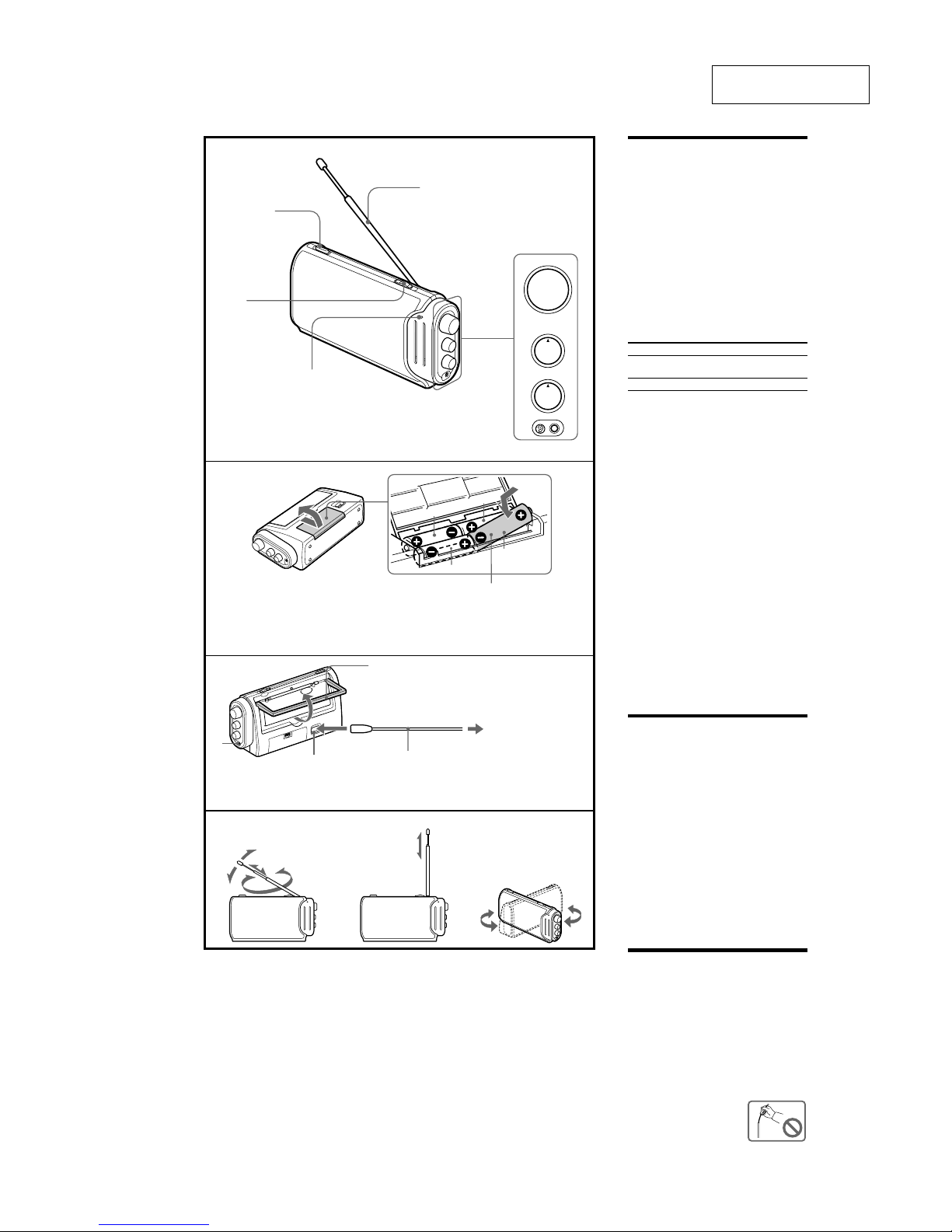
Installing the batteries
(See Fig. A)
1
Open the lid of the battery
compartment.
2
Install four R6 (sizeAA) batteries (not
supplied) with correct polarity.
3
Close the lid.
Note
When operating the unit on batteries, remove the AC
power cord from the AC IN jack. The unit cannot be
operated on batteries when the AC power cord is
connected to the AC IN jack.
Battery life (Approx. hours) (JEITA*)
When using FM SW AM(MW) LW
Sony alkaline 100 110 110 110
LR6 (size AA)
Sony R6 (size AA) 36 40 40 40
* Measured by JEITA (Japan Electronics and
Information Technology Industries Association)
Standards. The actual battery life may vary
depending on the circumstance of the unit.
Replacing batteries
When the sound becomes weak or distorted, replace
all the batteries with new ones.
Notes on batteries
• Do not charge the dry batteries.
• Do not carry the dry batteries with coins or other
metallic objects. It can generate heat if the positive
and negative terminals of the batteries are
accidentally contacted by a metallic object.
• Do not use different types of batteries at the same
time.
•When you replace the batteries, replace all with new
ones.
• When you are not going to use the unit for a long
time, remove the batteries to avoid damage from
battery leakage and corrosion.
House Current (See Fig. B)
1
Connect the AC power cord (supplied) to
the AC IN jack of the radio.
2
Plug into a wall outlet.
Note
Use only the supplied AC power cord.
Operating the
Radio
1
Press OPERATE ($) to turn on the
radio.
2
Select a desired band, and tune into a
station using TUNING.
TUNE (tuning) indicator lights up when a station
is tuned in.
3
Adjust the volume using VOL.
4
Adjust the tone to your preference using
TONE.
To obtain clear treble, turn to “HIGH”.
To reinforce bass, set to “LOW”.
•To turn off the radio, press OPERATE (4).
•To listen with an earphone connect the earphone
(not supplied) to the v(earphone) jack.
The speaker is deactivated when an earphone is
connected.
Improving the
Reception
(See Fig. C)
FM: Extend the telescopic antenna and
adjust the length and angle for the
best reception.
SW: Extend the telescopic antenna
vertically.
AM(MW)/LW: Rotate the unit horizontally for
optimum reception. A ferrite bar
antenna is built into the unit.
Note
Adjust the direction of the
antenna by holding the bottom of
it. The antenna can be damaged
when you move the antenna with
excessive force.
Telescopic antenna
Antenne télescopique
Teleskopantenne
Antena telescópica
Antenna telescopica
AC power cord (supplied)
Cordon d’alimentation secteur
Netzkabel (mitgeliefert)
Cable de alimentación de ca (suministrado)
Cavo di alimentazione CA (in dotazione)
Carrying handle
Poigné de transport
Tragegriff
Asa de transporte
Maniglia di trasporto
v
AM (MW)/LW
AM (PO)/GO
FM
UKW
SW
OC
KW
AC IN
Band
Gamme
Wellenbereich
Banda
Banda
TUNE indicator
Indicateur TUNE
TUNE-Anzeige
Indicador de sintonia (TUNE)
Indicatore TUNE
To a wall outlet
Vers une prise murale
An eine Netzsteckdose
A la toma de pared
Alla presa di rete

4
ICF-704S
SECTION 2
DISASSEMBLY
Note : This set can be disassemble according to the following sequence.
2-1. CABINET (FRONT) ASSY
(Page 5)
SET
2-2. CHASSIS SECTION
(Page 5)
2-3. MAIN BOARD
(Page 6)
2-4. SETTING THE POINTER
(Page 6)

5
ICF-704S
2-2. CHASSIS SECTION
2-1. CABINET (FRONT) ASSY
Note : Follow the disassembly procedure in the numerical order given.
5
two BV tapping
screws
(B2.6)
6
two BV tapping
screws
(B2.6)
7
two BV tapping
screws
(B2.6)
8
screw
(M3)
9
qs
cabinet (rear) assy
qd
cabinet (front) assy
1
knob (TUNE)
0
antenna contact plate
4
transparent cover
claw
2
screw
(1.7)
3
two
screws
(1.7)
qa
CN1
handle
battery case lid
3
chassis section
1
Remove the two solderings.
2
two BV tapping
screws
(B2.6)

6
ICF-704S
2-4. SETTING THE POINTER
2-3. MAIN BOARD
4
BV tapping
scre
w
(B2.6)
2
screw
(M2.6)
3
VC drum
5
claw
6
claw
D2
7
81
two knobs (control)
9
chassis assy
0
MAIN board
VC drum
boss
boss
pointer
back plate
rack
rac
k
chassis
1. Rotate the VC drum in the direction of the arrow until it is stopped.
2. Fit the rack on the projection of the chassis.
3. Fit the back plate on the bosses and attach the plate.
4. Install the pointer.
• Setting the Pointer

7
ICF-704S
Put the lead-wir
e
antenna close to
the set.
AM RF signal
generator
400Hz, 30%
AM modulation
Output level: as low as possible
•Repeat the procedures in each adjustment several times, and the
frequency coverage and tracking adjustments should be finally
done by the trimmer capacitors.
SW FREQUENCY COVERAGE ADJUSTMENT
Adjust for a maximum reading on level meter
L7 5.85 MHz
CT3 18.25 MHz
SWTRACKING ADJUSTMENT
Adjust for a maximum reading on level meter
L6 5.85 MHz
CT2 18.25 MHz
SECTION 3
ELECTRICAL ADJUSTMENTS
SW SECTION
BAND switch : SW
telescopic
antenna terminal
10pF
AM RF signal
generator
400Hz, 30%
AM modulation
Output level: as low as possible
set
16
Ω
set
v
jack (J1)
level mete
r
•Repeat the procedures in each adjustment several times, and the
frequency coverage and tracking adjustments should be finally
done by the trimmer capacitors.
MW IF ADJUSTMENT
Adjust for a maximum reading on level meter
T1
455 kHz
MW FREQUENCY COVERAGE ADJUSTMENT
Adjust for a maximum reading on level meter
L5 520 kHz
CT1-2 1,650 kHz
MWTRACKING ADJUSTMENT
Adjust for a maximum reading on level meter
L4 600 kHz
CT1-1 1,400 kHz
MW SECTION
BAND switch : MW
16
Ω
set
v
jack (J1)
level mete
r

8
ICF-704S
telescopic
antenna terminal
0.01µF
FM RF signal
generator
22.5kHz frequency deviation
by 400Hz signal
Output level: as low as possible
set
16
Ω
set
v
jack (J1)
level mete
r
•Repeat the procedures in each adjustment several times, and the
frequency coverage and tracking adjustments should be finally
done by the trimmer capacitors.
FM FREQUENCY COVERAGE ADJUSTMENT
Adjust for a maximum reading on level meter
L3 86.5 MHz
CT1-4 109.5 MHz
FM TRACKING ADJUSTMENT
Adjust for a maximum reading on level meter
L1, 2 86.5 MHz
CT1-3 109.5 MHz
Adjustment Location: MAIN BOARD
FM SECTION
BAND switch : FM
L1,2
FM
TRACKING
ADJUSTMENT
L6
SW
TRACKING
ADJUSTMENT
CT2
SW
TRACKING
ADJUSTMENT
T1
MW
IF
ADJUSTMENT
L3
FM
FREQUENCY
COVERAGE
ADJUSTMEN
T
L5
MW
FREQUENCY
COVERAGE
ADJUSTMEN
T
L7
SW
FREQUENCY
COVERAGE
ADJUSTMEN
T
CT3
SW
FREQUENCY
COVERAGE
ADJUSTMEN
T
L4
MW
TRACKING
ADJUSTMENT
CT1-4
FM
FREQUENCY
COVERAGE
ADJUSTMENT
CT1-3
FM
TRACKING
ADJUSTMENT
CT1-2
MW
FREQUENCY
COVERAGE
ADJUSTMENT
CT1-1
MW
TRACKING
ADJUSTMENT
– MAIN BOARD (SIDE A) –
– MAIN BOARD (SIDE B) –
CV1
S1
RV1
RV2
J1

99
ICF-704S
SECTION 4
DIAGRAMS
4-1. NOTE FOR PRINTED WIRING BOARDS AND SCHEMATIC DIAGRAMS
THIS NOTE IS COMMON FOR PRINTEDWIRING
BOARDS AND SCHEMATIC DIAGRAMS.
(In addition to this, the necessary note is printed
in each block.)
For schematic diagrams.
Note:
•All capacitors are in µF unless otherwise noted. pF: µµF
50 WV or less are not indicated except for electrolytics
and tantalums.
•All resistors are in Ωand 1/4W or less unless otherwise
specified.
•f: internal component.
•C: panel designation.
For printed wiring boards.
Note:
•X: parts extracted from the component side.
•Y: parts extracted from the conductor side.
•a: Through hole.
•: Pattern from the side which enables seeing.
(The other layers' patterns are not indicated.)
•A: B+ Line.
•H: adjustment for repair.
•Total current is measured with power on.
•Power voltage is dc 6V and fed with regulated dc power
supply from battery terminal.
•Voltage is dc with respect to ground under no-signal
(detuned) condition.
no mark : FM
():MW
•Voltages are taken with aVOM(Inputimpedance10MΩ).
Voltage variations may be noted due to normal produc-
tion tolerances.
•Signal path.
F: FM
f: MW
Caution:
Pattern face side: Partsonthepatternfacesideseenfromthe
(Side B) pattern face are indicated.
Parts face side: Parts on the parts face side seen from the
(Side A) parts face are indicated.
Note: The components identified by mark 0or dotted line
with mark 0are critical for safety.
Replace only with part number specified.
Q
C
These are omitted
EB

1010
ICF-704S
1
A
B
C
D
E
F
G
H
I
J
234567891011 12 13 14
A
C11
CT2
CT3
BLK
ANT1
FM/SW TELESCOPIC
ANTENNA
BRN
RED
CV1
JC1
C10
R3
JW5
JW6
JW14
JW4
R7
C2
C8
C9
C4
C5
C6
R1
C15
CV1-4
CT1-4
(FM OSC)
CV1-3
L4
AM FERRITE ROD
BAR ANTENNA
CT1-3
(FM RF)
CV1-1
CT1-1
(AM RF)
CV1-2
CT1-2
(AM OSC)
L3
C13
C12
C17
C16
R8
RV1 S1
(BAND)
SW
MW
FM
VOL
RV2
TONE
CV1
TUNING
D2
TUNE
RV1
L5
L7
RV2
C39
R12
J1
R10
W2
SP1
SPEAKER
SP+
LED
METER
LED+B
+B
GND
RED
BLK
D2
SP-
GRY
RED
12
R5
C23
C22
C27
C24
CF4
C26
JW13
C35 C36
CF1
C31
B C E
Q3
Q4
D1
BP1
T1
CF3
CF2
Q2
B C E
Q1
B C E
B C E
JW9
JW8
C32
C30
IC1
BPF1
S1
S1-6S1-5
S1-4S1-3
S1-2S1-1
1
316
30
15
1
CN1
POWER
BOARD
W101
R2
C25
C29
C28
R6
C37
R13
C40
C42
C50
C34
C47
C33
C44
R9
C45
C43
C41
JW16
JW10
JW12
JW11
JW7
JW2
JW3
JW15
C14
C18
JW1
C1
L6
C48
GRY
RED
BRN
BLK
L2 L1
1-861-802- 11
MAIN BOARD
4-2. PRINTEDWIRING BOARD — MAIN SECTION —
(Page 11)
D1 A-8
D2 H-3
IC1 D-10
Q1 E-11
Q2 E-12
Q3 E-12
Q4 C-12
•Semiconductor
Location
Ref. No. Location

11 11
ICF-704S
4-3. PRINTEDWIRING BOARDS — POWER SECTION —
1
A
B
C
D
E
F
G
H
I
J
234567891011 12 13 14
W101
W102
C103
GRY
RED
BLK
BLK
GRY
RED
RED
BLK
BLK
RED
GRY
BLK
RED
BLK
BLK
BLK
GRY
RED
1-861-816- 11
1-861-814- 11
1-861-815- 11
DRY BATTERY
SIZE "AA"
(IEC DESIGNATION LR6)
4PCS,6V
W102
1
12
3
1
3
AC1
AC2
AC1
AC1
W103
S101 S101
OPERATE
ON STANDBY
1
3
1
3
W103
T101
J101
~ AC IN
GRY
BLK
C101
R101
D101
D102
C102
POWER BOARD
AC INLET BOARD
SWITCH
BOARD
A
MAIN
BOARD
CN1
(Page 10)

1212
ICF-704S
CF3CF2
IC1
CF4
RV1
T1
CF1
RV2
SP1
BPF1
R2
CV1-3
CT1-3
C2
L4
CT1-1
C8C9
S1-3
S1-4
CV1-1
JW1
R3
C10
L6
C11C1
S1-5
C48
JW15
JC1
JW4
JW14
ANT1
D1
BP1
JW5
C24
S1-2
JW7
JW13
R8
C27
C25
C26
L3
CV1-4
CT1-4
C4 C5 C6 R1
JW2
CV1-2
S1-1
C18
C12
C13
C14
C15
C17 C16
CT1-2
L5
JW3
R5 C23 C22 CT3 L7
R6 R7
JW6
JW9
S1-6
Q4
JW8
Q3
C37
R13
C47
C36
Q1
Q2
C31
C30
C32
C35
C33
C39
JW10
C41
C43
C42
C40
C44
C50
JW12
R10
R9 JW11
T101
C101
D101
D102
C102
C103
S101
R101
J1
C29
L1
L2
C28
D2
JW16
C45
R12
W103 W103
W102 W102
W2
CN1
W101
J101
CT2
4-4. SCHEMATIC DIAGRAM

13
ICF-704S
1
2
3
4
5
13
6
13
14
7
15
33
8
16
17
18
19
L4
D2
#1
SP1
21
32
20
22
23
23
24
26 26
28
25
9
10
11
12
29
29
29
30
31
27
Ref. No. Part No. Description Remark
5-1. CABINET (FRONT) SECTION
Ref. No. Part No. Description Remark
13-264-585-11 SLIDER (BAND SELECTION)
23-264-608-01 SPRING (BAND)
33-264-589-01 GEAR, MIDWAY
43-264-581-01 CHASSIS
53-264-588-01 SHAFT (TUNE)
63-264-591-01 RACK
73-265-121-01 PLATE, BACK
83-264-590-01 POINTER
93-264-586-01 DRUM (A), VC
10 3-264-587-01 DRUM (B), VC
11 3-266-375-01 SPRING (DRUM)
12 3-252-831-01 SCREW (M2.6), (+) P
13 3-252-825-01 SCREW (1.7)
14 3-266-360-01 SPRING (TUNING)
15 3-264-583-01 KNOB (TUNE)
16 3-264-584-01 KNOB (CONTROL)
17 3-252-747-01 SPRING, RING
18 3-264-582-21 COVER, TRANSPARENT
19 X-2022-199-1 CABINET (FRONT) SUB ASSY
20 2-024-240-01 SPACER (BOSS)
21 3-264-611-01 KNOB (BAND) 3B
22 3-264-593-01 BUTTON (POWER)
23 3-252-828-01 SCREW (B2.6), (+) PWH TAPPING
*24 A-4547-217-A MAIN BOARD, COMPLETE
25 3-264-614-01 HOLDER (ANT)
26 3-252-827-01 SCREW (B2.6), (+) BV TAPPING
27 3-264-607-01 TERMINAL, LED CONTACT
28 3-267-201-01 CUSHION (BATTERY CASE LID)
29 3-254-140-01 SCREW (B2.6), (+) BV TAPPING
30 3-264-613-01 LID, BATTERY CASE
31 2-048-404-11 CUSHION (GEAR)
32 3-553-567-00 CUSHION
33 3-831-441-11 CUSHION (B)
D2 8-719-038-29 LED SLP-181B-51 (TUNE)
L4 1-754-132-21 ANTENNA, FERRITE-ROD (MW)
SP1 1-825-789-11 SPEAKER (10cm)
#1 7-671-112-11 BALL, STEEL
SECTION 5
EXPLODEDVIEWS
NOTE:
•The mechanical parts with no reference
number in the exploded views are not supplied.
•Items marked “*” are not stocked since
they are seldom required for routine service.
Some delay should be anticipated
when ordering these items.
•Color Indication of Appearance Parts
Example :
KNOB, BALANCE (WHITE) ... (RED)
Parts Color Cabinet’s Color
•Accessories are given in the last of this
parts list.
RR
The components identified by
mark 0or dotted line with mark
0are critical for safety.
Replace only with part number
specified.

14
ICF-704S
5-2. CABINET (REAR) SECTION
Ref. No. Part No. Description RemarkRef. No. Part No. Description Remark
51 3-264-610-01 CABINET (REAR)
52 3-264-617-01 TERMINAL (+–), BATTERY
53 3-264-619-01 SPRING (HANDLE)
54 3-252-827-01 SCREW (B2.6), (+) BV TAPPING
55 3-264-616-01 TERMINAL (–), BATTERY
*56 1-861-815-11 AC INLET BOARD
*57 1-861-814-11 POWER BOARD
58 3-248-610-01 TERMINAL (+), BATTERY
59 3-228-709-01 PLATE, ANTENNA CONTACT
60 3-264-618-01 SHAFT (HANDLE)
*61 1-861-816-11 SWITCH BOARD
62 3-264-612-01 HANDLE
63 3-252-833-01 SCREW (M3), (+) P
64 3-014-055-01 FOOT, RUBBER
65 3-043-480-01 SHEET (C), INSULATING
66 3-831-441-11 CUSHION (B)
ANT1 1-501-222-91 ANTENNA, TELESCOPIC (FM)
0J101 1-526-838-31 INLET, AC 2P (-AC IN)
0T101 1-443-240-11 TRANSFORMER, POWER
The components identified by
mark 0or dotted line with mark.
0are critical for safety.
Replace only with part number
specified.
51
52
65
53
54
54
54
54
55
56
57
J101
ANT1
T101
not supplied
not supplied
58
59
60
61
62
64
63
66

15
ICF-704S
SECTION 6
ELECTRICAL PARTS LIST
Ref. No. Part No. Description Remark Ref. No. Part No. Description Remark
*1-861-815-11 AC INLET BOARD
**************
< AC INLET >
0J101 1-526-838-31 INLET, AC 2P (-AC IN)
*************************************************************
*A-4547-217-A MAIN BOARD, COMPLETE
*********************
3-252-827-01 SCREW (B2.6), (+) BV TAPPING
3-264-607-01 TERMINAL, LED CONTACT
3-264-614-01 HOLDER (ANT)
< BPF >
BPF1 1-236-022-11 FILTER, BAND PASS
< CAPACITOR >
C1 1-162-964-11 CERAMIC CHIP 0.001uF 10% 50V
C2 1-162-919-11 CERAMIC CHIP 22PF 5% 50V
C4 1-162-996-11 CERAMIC CHIP 7PF 0.5PF 50V
C5 1-162-997-11 CERAMIC CHIP 10PF 0.5PF 50V
C6 1-162-913-11 CERAMIC CHIP 8PF 0.5PF 50V
C8 1-162-915-11 CERAMIC CHIP 10PF 0.5PF 50V
C9 1-162-915-11 CERAMIC CHIP 10PF 0.5PF 50V
C10 1-162-970-11 CERAMIC CHIP 0.01uF 10% 25V
C11 1-162-908-11 CERAMIC CHIP 3PF 0.25PF 50V
C12 1-164-230-11 CERAMIC CHIP 220PF 5% 50V
C13 1-162-927-11 CERAMIC CHIP 100PF 5% 50V
C14 1-162-923-11 CERAMIC CHIP 47PF 5% 50V
C15 1-162-919-11 CERAMIC CHIP 22PF 5% 50V
C16 1-162-945-11 CERAMIC CHIP 22PF 5% 50V
C17 1-162-912-11 CERAMIC CHIP 7PF 0.5PF 50V
C18 1-162-968-11 CERAMIC CHIP 0.0047uF 10% 50V
C22 1-162-997-11 CERAMIC CHIP 10PF 0.5PF 50V
C23 1-162-996-11 CERAMIC CHIP 7PF 0.5PF 50V
C24 1-126-964-11 ELECT 10uF 20% 50V
C25 1-162-970-11 CERAMIC CHIP 0.01uF 10% 25V
C26 1-126-963-11 ELECT 4.7uF 20% 50V
C27 1-164-156-11 CERAMIC CHIP 0.1uF 25V
C28 1-162-927-11 CERAMIC CHIP 100PF 5% 50V
C29 1-162-970-11 CERAMIC CHIP 0.01uF 10% 25V
C30 1-162-970-11 CERAMIC CHIP 0.01uF 10% 25V
C31 1-126-963-11 ELECT 4.7uF 20% 50V
C32 1-126-964-11 ELECT 10uF 20% 50V
C33 1-115-156-11 CERAMIC CHIP 1uF 10V
C35 1-164-227-11 CERAMIC CHIP 0.022uF 10% 25V
C36 1-164-227-11 CERAMIC CHIP 0.022uF 10% 25V
C37 1-164-227-11 CERAMIC CHIP 0.022uF 10% 25V
C39 1-165-176-11 CERAMIC CHIP 0.047uF 10% 16V
C40 1-162-964-11 CERAMIC CHIP 0.001uF 10% 50V
C41 1-126-947-11 ELECT 47uF 20% 35V
C42 1-115-156-11 CERAMIC CHIP 1uF 10V
C43 1-126-925-91 ELECT 470uF 20% 10V
C44 1-115-156-11 CERAMIC CHIP 1uF 10V
C45 1-126-925-91 ELECT 470uF 20% 10V
C47 1-115-156-11 CERAMIC CHIP 1uF 10V
C48 1-162-964-11 CERAMIC CHIP 0.001uF 10% 50V
C50 1-115-156-11 CERAMIC CHIP 1uF 10V
< FILTER >
CF1 1-795-157-11 FILTER, CERAMIC
CF2 1-577-325-81 FILTER, CERAMIC
CF3 1-577-325-81 FILTER, CERAMIC
CF4 1-577-325-81 FILTER, CERAMIC
< CONNECTOR >
*CN1 1-785-668-11 PIN, CONNECTOR (PC BOARD) 2P
< VARIABLE CAPACITOR >
CT1 1-141-583-22 CAP, VAR
CV1 1-141-583-22 CAP, VAR (TUNING)
< TRIMMER >
CT2 1-141-304-21 CAP, CERAMIC TRIMMER 10PF
CT3 1-141-304-21 CAP, CERAMIC TRIMMER 10PF
< DIODE >
D1 8-719-062-51 DIODE 1PS226-115
< IC >
IC1 8-752-037-02 IC CXA1019S
< JACK >
J1 1-563-836-21 JACK (v)
< JUMPER RESISTOR >
JC1 1-216-864-11 SHORT CHIP 0
NOTE:
•Due to standardization, replacements in
the parts list may be different from the
parts specified in the diagrams or the
components used on the set.
•RESISTORS
All resistors are in ohms.
METAL:Metal-film resistor.
METAL OXIDE: Metal oxide-film resistor.
F:nonflammable
•Abbreviation
AUS:Australian model
•Items marked “*” are not stocked since
they are seldom required for routine service.
Some delay should be anticipated
when ordering these items.
• SEMICONDUCTORS
In each case, u : µ, for example:
uA.. : µA.. uPA.. : µPA..
uPB.. : µPB.. uPC.. : µPC.. uPD.. : µPD..
•CAPACITORS
uF : µF
•COILS
uH : µH
The components identified by
mark 0or dotted line with mark.
0are critical for safety.
Replace only with part number
specified.
When indicating parts by reference
number, please include the board.
AC INLET MAIN

16
ICF-704S
The components identified by
mark 0or dotted line with mark.
0are critical for safety.
Replace only with part number
specified.
Ref. No. Part No. Description Remark Ref. No. Part No. Description Remark
< COIL >
L1 1-428-291-11 COIL, AIR-CORE
L2 1-428-291-11 COIL, AIR-CORE
L3 1-428-222-11 COIL, FM OSC
L4 1-754-132-21 ANTENNA, FERRITE-ROD (MW)
L5 1-406-092-31 COIL, OSC (MW)
L6 1-456-747-11 COIL, SW (ANT)
L7 1-406-093-31 COIL, OSC (SW)
< TRANSISTOR >
Q1 8-729-905-35 TRANSISTOR 2SC4081-R
Q2 8-729-029-14 TRANSISTOR DTC144EUA-T106
Q3 8-729-029-14 TRANSISTOR DTC144EUA-T106
Q4 8-729-029-14 TRANSISTOR DTC144EUA-T106
< RESISTOR >
R1 1-216-833-11 METAL CHIP 10K 5% 1/10W
R2 1-216-821-11 METAL CHIP 1K 5% 1/10W
R3 1-216-841-11 METAL CHIP 47K 5% 1/10W
R5 1-216-833-11 METAL CHIP 10K 5% 1/10W
R6 1-216-825-11 METAL CHIP 2.2K 5% 1/10W
R7 1-216-813-11 METAL CHIP 220 5% 1/10W
R8 1-216-821-11 METAL CHIP 1K 5% 1/10W
R9 1-216-825-11 METAL CHIP 2.2K 5% 1/10W
R10 1-216-829-11 METAL CHIP 4.7K 5% 1/10W
R12 1-216-805-11 METAL CHIP 47 5% 1/10W
R13 1-216-845-11 METAL CHIP 100K 5% 1/10W
< VARIABLE RESISTOR >
RV1 1-227-647-11 RES, VAR, CARBON 50K (VOL)
RV2 1-227-646-11 RES, VAR, CARBON 10K (TONE)
< SWITCH >
S1 1-571-170-21 SWITCH, SLIDE (BAND)
< TRANSFORMER >
T1 1-404-902-51 TRANSFORMER, IF
*************************************************************
*1-861-814-11 POWER BOARD
*************
< CAPACITOR >
C101 1-164-156-11 CERAMIC CHIP 0.1uF 25V
C102 1-164-156-11 CERAMIC CHIP 0.1uF 25V
C103 1-126-927-11 ELECT 2200uF 20% 10V
< DIODE >
D101 8-719-063-79 DIODE 1N4002B
D102 8-719-063-79 DIODE 1N4002B
*************************************************************
*1-861-816-11 SWITCH BOARD
*************
< RESISTOR >
R101 1-216-833-11 METAL CHIP 10K 5% 1/10W
< SWITCH >
S101 1-572-176-21 SWITCH, PUSH (1 KEY) (OPERATE)
*************************************************************
MISCELLANEOUS
***************
ANT1 1-501-222-91 ANTENNA, TELESCOPIC (FM)
D2 8-719-038-29 LED SLP-181B-51 (TUNE)
SP1 1-825-789-11 SPEAKER (10cm)
0T101 1-443-240-11 TRANSFORMER, POWER
*************************************************************
ACCESSORIES
************
01-828-834-11 CORD, POWER
3-266-178-11 MANUAL, INSTRUCTION (ENGLISH,FRENCH,
GERMAN,SPANISH,ITALIAN,DUTCH,SWEDISH,
PORTUGUESE,FINNISH)
MAIN POWER SWITCH

17
ICF-704S
MEMO

18
ICF-704S
REVISION HISTORY
Clicking the version allows you to jump to the revised page.
Also, clicking the version at the upper on the revised page allows you to jump to the next revised page.
Ver. Date Description of Revision
1.0 2004. 04 New
Other manuals for ICF-704S
1
Table of contents
Other Sony Radio manuals

Sony
Sony SRF-S83 User manual

Sony
Sony ICF-403S User manual

Sony
Sony ICF-306 User manual

Sony
Sony SRF-M606 User manual

Sony
Sony ICF-B88 User manual

Sony
Sony CRF-5080 User manual

Sony
Sony SRF-HM03V - S2 Sports Stereo Headphone Walkman Headband... User manual

Sony
Sony ICF-40 User manual

Sony
Sony Sports Walkman SRF-M78 User manual

Sony
Sony Walkman SRF-M97 User manual