Sony XDR-S3HD - HD / AM User manual

1
Ver. 1.0 2007. 05
SERVICE MANUAL
US Model
XDR-S3HD
SPECIFICATIONS
Time display 12-hour system
Frequency range FM : 87.5 – 108 MHz
AM : 530 – 1,710 kHz
Speaker Approx. 6.6 cm (2 5/8 inches) dia. 4 Ω
Output i(headphone) jack (φ3.5 mm stereo minijack)
Input LINE IN jack (φ3.5 mm stereo minijack)
Antenna terminal 75 Ωantenna terminal for FM
Antenna terminal forAM
Power output 2.8 W + 2.8 W (at 10% harmonic distortion)
Power requirements 120 VAC, 60 Hz
Dimensions Approx. 300 ×120 ×169 mm (w/h/d)
(11 7/8 ×4 3/4 ×6 3/4 inches) not incl. projecting
parts and controls
Mass Approx. 3.6 kg (7 lb 15.8 oz) incl. power supply unit
Supplied accessories Remote commander (1)
FM wire antenna (1)
FM dipole antenna (1)
AM loop antenna (1)
Audio connecting cable (1)
Design and specifications are subject to change
without notice.
Sony Corporation
Personal Audio Division
Published by Sony Techno Create Corporation
9-887-734-01
2007E04-1
© 2007. 05
FM/AM DIGITAL RADIO
HD Radio Broadcasting was approved by the Federal
Communications Commission in October 2002 as the system
for digital AM and FM broadcasting in the U.S.
HD Radio technology features include:
–Static-free, clear radio reception.
–FM Multicasting – the ability to broadcast multiple program
streams over a single FM frequency.
–Avariety of “data services,” including text-based
information – artist name, song title, etc. scrolled across your
receiver display.
–Digital broadcasts in the same frequencies as analog
broadcasts; listeners do not need to learn a new station
number and today’s stations remain at their current place on
the dial.
HD Radio technology is developed and licensed by iBiquity
Digital Corporation and supported by the leaders of the
broadcasting, consumer electronics and automotive industries.
HD RadioTM Technology Manufactured Under License From
iBiquity Digital Corporation. iBiquity Digital, the HD Radio
logo, and the HD logo are registered trademarks of iBiquity
Digital Corporation. HD RadioTM is a trademark of iBiquity
Digital Corporation. U.S. and Foreign Patents.

2
XDR-S3HD
SERVICE NOTES
Notes on Chip Component Replacement
•Never reuse a disconnected chip component.
•Notice that the minus side of a tantalum capacitor may be dam-
aged by heat.
zUNLEADED SOLDER
Boards requiring use of unleaded solder are printed with the lead
free mark (LF) indicating the solder contains no lead.
(Caution: Some printed circuit boards may not come printed with
the lead free mark due to their particular size.)
: LEAD FREE MARK
Unleaded solder has the following characteristics.
• Unleaded solder melts at a temperature about 40°C higher than
ordinary solder.
Ordinary soldering irons can be used but the iron tip has to be
applied to the solder joint for a slightly longer time.
Soldering irons using a temperature regulator should be set to
about 350°C.
Caution: The printed pattern (copper foil) may peel away if the
heated tip is applied for too long, so be careful!
•Strong viscosity
Unleaded solder is more viscous (sticky, less prone to flow)
than ordinary solder so use caution not to let solder bridges
occur such as on IC pins, etc.
•Usable with ordinary solder
It is best to use only unleaded solder but unleaded solder may
also be added to ordinary solder.
SAFETY-RELATED COMPONENT WARNING!!
COMPONENTS IDENTIFIED BY MARK 0OR DOTTED LINE
WITH MARK 0ON THE SCHEMATIC DIAGRAMS AND IN
THE PARTS LIST ARE CRITICAL TO SAFE OPERATION.
REPLACE THESE COMPONENTS WITH SONY PARTS WHOSE
PART NUMBERS APPEAR AS SHOWN IN THIS MANUAL OR
IN SUPPLEMENTS PUBLISHED BY SONY.
TABLE OF CONTENTS
1. GENERAL ........................................................................... 3
2. DISASSEMBLY
2-1. Panel (Front) Assy ............................................................... 6
2-2. DC Fan (M950) ................................................................... 7
2-3. Wires ................................................................................... 7
2-4. Chassis Assy........................................................................ 8
2-5. MAIN Board ....................................................................... 8
2-6. POWER Board .................................................................... 9
2-7. KEY Board .......................................................................... 9
2-8. VOL Board, TUNE Board ................................................ 10
2-9. Assembly of the Power Cord ............................................ 10
3. DIAGRAMS
3-1. Block Diagram .................................................................. 11
3-2. Printed Wiring Board – Main Section –............................ 13
3-3. Schematic Diagram – Main Section –............................... 14
3-4. Printed Wiring Boards – Power Section –......................... 15
3-5. Schematic Diagram – Power Section –............................. 16
3-6. Printed Wiring Board – Micon Section –.......................... 17
3-7. Schematic Diagram – Micon Section –............................. 18
3-8. Printed Wiring Boards – Key Section – ............................ 19
3-9. Schematic Diagram – Key Section – ................................ 20
4. EXPLODED VIEWS
4-1. Main Section ..................................................................... 25
4-2. Front Panel Section ........................................................... 26
4-3. KEY Board Section........................................................... 27
4-4. Cabinet Section ................................................................. 28
4-5. Chassis Section ................................................................. 29
5. ELECTRICAL PARTS LIST ........................................ 30
1.5 k
Ω
0.15 µFAC
voltmeter
(0.75 V)
To Exposed Metal
Parts on Set
Earth Ground
SAFETY CHECK-OUT
After correcting the original service problem, perform the fol-
lowing safety check before releasing the set to the customer:
Check the antenna terminals, metal trim, “metallized” knobs,
screws, and all other exposed metal parts for AC leakage.
Check leakage as described below.
LEAKAGE TEST
The AC leakage from any exposed metal part to earth ground
and from all exposed metal parts to any exposed metal part
having a return to chassis, must not exceed 0.5 mA (500
microampers.).
Leakage current can be measured by any one of three methods.
1. A commercial leakage tester, such as the Simpson 229 or
RCA WT-540A. Follow the manufacturers’ instructions to use
these instruments.
2. A battery-operated AC milliammeter. The Data Precision 245
digital multimeter is suitable for this job.
3. Measuring the voltage drop across a resistor by means of a
VOM or battery-operated AC voltmeter. The “limit” indica-
tion is 0.75 V, so analog meters must have an accurate low-
voltage scale. The Simpson 250 and Sanwa SH-63Trd are
examples of a passive VOM that is suitable. Nearly all bat-
tery operated digital multimeters that have a 2 V AC range
are suitable. (See Fig. A)
Fig. A. Using an AC voltmeter to check AC leakage.

3
XDR-S3HD
SECTION 1
GENERAL This section is extracted
from instruction manual.
Tip
The preset can be selected by pressing the number
button of the remote commander. Press ENTER after
the preset number is selected.
—Scan tuning
The unit will automatically scan the selected band.
In HD scan, HD Radio stations are scanned.
1Press POWER to turn on the radio.
2Press BAND to select the band AM or FM.
3Press MENU to show the menu display.
4Turn TUNE/SELECT clockwise or
counterclockwise to select “SCAN” or “HD
SCAN,” then press ENTER.
Scanning of the selected band starts.
When a station is received, scanning pauses for 3
seconds and then continues.
5When the unit tunes in to the desired station,
do any of the following operations to stop
scanning.
–Press ENTER on the unit or remote commander.
–Press SCAN or HD SCAN on the remote
commander.
6If necessary, turn TUNE/SELECT
clockwise or counterclockwise to tune in to
the station more precisely.
7Adjust the volume using VOLUME.
Tip
You can scan a station directly by pressing SCAN or
HD SCAN on the remote commander.
To listen with the
headphones
You can enjoy the radio and external equipment
connected to the line in by the headphones (not
supplied). Connect the headphones (not supplied) to the
i(headphone) jack. The speaker is deactivated when
the headphones are connected.
Changing the
display mode and
settings
To change the display mode
Press DISPLAY.
The display changes as follows:
When an analog radio station is received
x
AField strength level indicator
BPreset number*
CBand
DFrequency
ECurrent time
*When you tune in a station by selecting a preset
number.
When an analog FM broadcast that supports
RBDS (Radio Broadcast Data System) is
received
x
x
x
POWER
VOLUME TUNE/SELECT
SLEEP BAND PRESET TONE DISPLAY MENU ENTER
RADIO
/
LINE IN
AM FM XMSIRIUS
SLEEP ALARM
ANTENNA
AM
RESET
LINE IN
FM
SLEEPALARM
POWER
123
456
78
0
9
SCANMENU
HD SCAN
BAND
PRESET
TONE
DISPLAY
BRIGHT
VOL
RADIO/
LINE IN
TUNE/
SELECT
ENTER
A
B
AC power cord
The number 5 and the VOL +
buttons have a tactile dot.
Size AAA (R03)
×2
Preparing the
remote commander
Installing the batteries into the remote
commander (See Fig. B)
Insert two size AAA (R03) batteries (not supplied).
When to replace the batteries
With normal use, the batteries should last for about six
months. When the remote commander no longer
operates the unit, replace all the batteries with new ones.
Notes
•Do not charge dry batteries.
•When you are not going to use the remote commander
for a long time, remove the batteries to avoid any
damage caused by leakage and corrosion.
Setting the clock
1Plug in the unit.
The display will flash “AM 12:00.”
2Press MENU to show the menu display.
3Turn TUNE/SELECT clockwise to select
“TIME SET,” then press ENTER.
The hour will start to flash in the display.
4Turn TUNE/SELECT clockwise or
counterclockwise until current hour appears in
the display, then press ENTER.
The hour is set and the minutes start to flash.
5Repeat step 4 to set the minute.
Note
If you do not set the menu within 65 seconds, the setting
mode is canceled.
To change the display to the
daylight saving time
(summer time) indication
1Press MENU to show the menu display.
2Turn TUNE/SELECT clockwise or
counterclockwise to select “DST,” then press
ENTER.
3Turn TUNE/SELECT counterclockwise to
select “ON,” then press ENTER.
“
” appears and the time indication changes to
summer time.
To deactivate the DST function, select “OFF” in step 3.
Playing the radio
—Manual tuning
1Press POWER to turn on the radio.
If “LINE IN” is displayed, press RADIO/LINE IN
so that the band (AM or FM) appears.
2Press BAND to select the band AM or FM.
3Turn TUNE/SELECT clockwise or
counterclockwise to tune in to a desired
frequency.
A beep sounds when the minimum frequency of
each band is received during tuning.
4Adjust the volume using VOLUME.
Tip
To attenuate the volume, turn VOLUME
counterclockwise quickly.
Note
The frequency cannot be input with the number buttons
of the remote commander.
—Preset tuning
You can preset 20 stations each for AM and FM.
Presetting a station
1Follow steps 1 to 3 in “Manual tuning” to
tune the frequency you wish to preset.
2Press and hold PRESET for a few seconds.
You will hear a beep.
3Turn TUNE/SELECT clockwise or
counterclockwise to select the preset number,
then press ENTER.
The frequency is stored in the selected preset
number and you will hear a beep.
To preset another station, repeat these steps.
Note
If you try to store another station in the same preset
number, the previously stored station will be replaced.
Tuning in to a station
1Press POWER to turn on the radio.
2Press BAND to select the band AM or FM.
3Press PRESET.
The preset number appears in upper left in the
display.
4Turn TUNE/SELECT clockwise or
counterclockwise to select the preset number.
5Adjust the volume using VOLUME.

4
XDR-S3HD
or
AField strength level indicator
BPreset number*
CBand
DStation name
Name of station currently tuned in.
EFrequency
FText information
Text information transmitted from station.
GCurrent time
*When you tune in a station by selecting a preset
number.
Note
The display item differs depending on the content of a
broadcast or the station.
When an HD Radio station is received
x
or
x
If you press DISPLAY for 2 seconds while the
display above appears, the beep is heard and the
scroll speed of the display item becomes slow.
To return to normal scroll speed, press DISPLAY
again for 2 seconds.
AHD indicator
Lights: HD Radio reception level is sufficient
(indicator flashes momentarily, and then
stays lit).
The sound changes from analog to digital.
Flashes: HD Radio reception level is too low.
The sound stays analog.
If a HD Radio station signal is very weak, the
indicator will not flash.
BField strength level indicator
CPreset number*
DCurrent station’s call letters
EBand
FStation name and information
GTitle/Artist name
HSub channel (FM only)
Appears when HD Radio broadcasts multiple
program.
Turn TUNE/SELECT clockwise or
counterclockwise to select a sub channel.
IFrequency
JCurrent time
KText information
*When you tune in a station by selecting a preset
number
Note
The display item differs depending on the content of a
broadcast or the station.
To change the display
settings (BRIGHTNESS/
CONTRAST)
1
Press MENU to show the menu display.
2
Turn TUNE/SELECT clockwise or
counterclockwise to select “BRIGHTNESS”
or “CONTRAST,” then press ENTER.
3
Turn TUNE/SELECT clockwise or
counterclockwise to select the setting or to
adjust the level, then press ENTER.
BRIGHTNESS:
The brightness of the display is selected from
“HIGH,” “MIDDLE” or “LOW.”
CONTRAST:
The contrast of the display can be adjusted by 11
levels.
Note
If you do not set the menu within 10 seconds, the setting
mode is canceled.
Tip
You can adjust “BRIGHTNESS” directly by pressing
BRIGHT on the remote commander.
Adjusting the tone
1
Press POWER to turn on the radio.
2
Press TONE to show the tone setting
display.
3
Turn TUNE/SELECT clockwise or
counterclockwise to set “TREBLE,” then
press TONE.
4
Turn TUNE/SELECT clockwise or
counterclockwise to set “BASS,” then press
TONE.
5
Turn TUNE/SELECT clockwise or
counterclockwise to set “SURROUND,” then
press TONE.
Tip
The adjustable range of “TREBLE” and “BASS” is from
–6 to +6.
“SURROUND” switches “ON” or “OFF.”
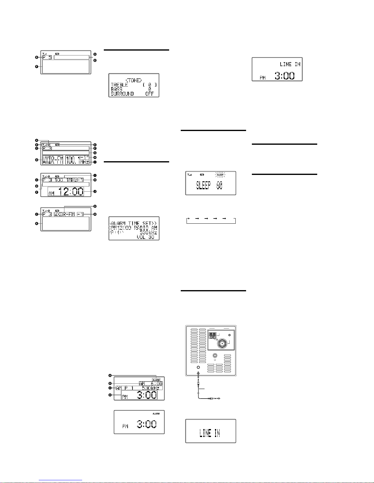
Setting the alarm
You can set the unit to turn on automatically at a preset
time. The alarm can be set, even if the unit is off.
To adjust the hour and minute, see “Setting the clock.”
To set the alarm time
1
Press MENU to show the menu display.
2
Turn TUNE/SELECT clockwise or
counterclockwise to select “ALARM TIME
SET,” then press ENTER.
The hour sign starts flashing.
Example of display when unit is off
3
Turn TUNE/SELECT clockwise or
counterclockwise to set the hour, then press
ENTER.
The minute sign starts flashing.
4
Turn TUNE/SELECT clockwise or
counterclockwise to set the minutes, then
press ENTER.
The source sign starts flashing.
5
Turn TUNE/SELECT clockwise or
counterclockwise to select the source from
“RADIO AM,” “RADIO FM,” “LINE IN” or
“BUZZER,” then press ENTER.
If you select “RADIO AM,” “RADIO FM” or
“LINE IN” continue the following steps.
6
Turn TUNE/SELECT clockwise or
counterclockwise to select the preset number,
then press ENTER.
If you selected “LINE IN” in step 5, this step is not
necessary.
7
Turn TUNE/SELECT clockwise or
counterclockwise to set the volume, then
press ENTER.
To set the alarm
1
Press MENU to show the menu display.
2
Turn TUNE/SELECT clockwise or
counterclockwise to select “ALARM SET,”
then press ENTER.
3
Turn TUNE/SELECT counterclockwise to
select “ON,” then press ENTER.
“ALARM” appears in the display.
Example of display when unit is off
If you press DISPLAY while the display above
appears, the display changes to the following.
To return to the previous display, press DISPLAY
again.
AALARM indicator
BAlarm setting time
CAlarm setting (Source, Frequency, etc.)
DCurrent time
To deactivate the alarm function, turn
TUNE/SELECT
clockwise to select “OFF” in step 3.
To stop the alarm
Press POWER on the unit or remote commander.
Tips
• To enter “ALARM TIME SET” mode directly, press
and hold ALARM on the remote commander for 2
seconds.
• You can activate or deactivate the alarm function
directly by pressing ALARM on the remote
commander.
Notes
• If you do not set the menu within 10 seconds, the
setting mode is canceled.
• If you do not operate the unit for 60 minutes after
alarm sounds, the power is turned off.
• If you select “LINE IN” source in “ALARM TIME
SET,” start playback on the external equipment. You
cannot control the external equipment from this unit.
Setting the sleep
timer
You can enjoy falling asleep to the radio using the built-
in sleep timer that turns off the radio automatically after
a preset duration.
1
Press SLEEP.
“SLEEP” and the digits for the sleep timer duration
appear.
If you press SLEEP while the unit is turned off, the
unit is turned on.
2
Press SLEEP repeatedly to select the desired
sleep timer setting.
Each press changes the setting time as follows:
60 45 1530 OFF
A beep sounds when the display returns to “SLEEP
60.”
After about 4 seconds, “SLEEP” lights in the display
when the duration time is set.
The unit automatically turns off when the duration time
is passed.
To change the sleep timer setting
You can press SLEEP repeatedly to select the desired
sleep timer setting even after the sleep timer has been
activated.
To deactivate the sleep timer
Press POWER to turn off the unit before the setting
time has elapsed, or press SLEEP repeatedly to set the
sleep timer to “SLEEP OFF” in step 2.
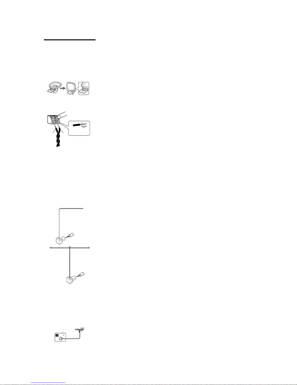
Listening to the
external equipment
1
Connect the LINE IN jack of the unit to the
line out jack or headphone jack of the external
equipment using the audio connecting cable
(supplied).
ANTENNA
AM
RESET
LINE IN
FM
Audio connecting cable
(supplied)
To external
equipment
2
Press POWER to turn on the radio.
3
Press RADIO/LINE IN to select “LINE
IN” in the display.
4
Play the equipment connected to the LINE IN
jack.
5
Adjust the volume using VOLUME.
Tip
To display the current time, press DISPLAY.
To return to the radio
Press RADIO/LINE IN.
The band (AM or FM) is shown in the display.
Notes
• Refer also to the connected equipment’s manual.
• The supplied audio connecting cable may not be used
with some external equipment. In this case, use a cord
suitable for the external equipment you are using.
•When you listen to the radio with external equipment
connected, turn off the connected equipment because
noise may be caused. If noise continues, even when
the equipment is turned off, disconnect and place the
external equipment away from the unit.
Resetting the unit
The RESET button is located on the rear of the unit.
Press this button with a pointed object if the radio fails
to function properly. The clock settings and stations you
have preset, etc., will revert to the factory preset.
Using the remote
commander
Buttons shared on both the remote commander and the
unit control the same functions.
VOL +/— buttons
To adjust the volume.
Press and hold the VOL – button for 2.5 seconds, the
volume becomes minimized.
ALARM button
Press to set the alarm to “ON” or “OFF.”
Press and hold for 2 seconds to enter “ALARM TIME
SET.”
HD SCAN button
The selected band is scanned, and receivable HD Radio
stations are received for 3 seconds in order of frequency.
SCAN button
The selected band is scanned, and receivable radio
stations are received for 3 seconds in order of frequency.
BRIGHT button
To adjust the brightness of the display.
Number buttons
To select a preset number (1 to 20).
Press ENTER after the preset number is selected.
If you input the number 0 or more than 21 and press
ENTER, “ERROR” appears in the display.

5
XDR-S3HD
Connecting the
antenna
To connect the AM loop
antenna
The shape and the length of the antenna is designed to
receive AM signals. Do not dismantle or roll up the
antenna.
1Remove only the loop part from the plastic
stand.
2Set up the AM loop antenna.
3Connect the cords to the AM antenna
terminals.
Cord (A) or cord (B) can be connected to either
terminal.
AB
Only insert up
to here.
4Make sure the AM loop antenna is connected
firmly by pulling softly.
Adjusting the AM loop antenna
Find a place and an orientation that provide good
reception.
•Do not place the AM loop antenna near the unit or
other AV equipment, as noise may result.
•If you use an external polarized AM antenna, be sure
to connect the ground cord to the Uterminal. The
supplied AM antenna cord has no polarity.
Tip
Adjust the direction of the AM loop antenna for best AM
broadcast sound.
To connect the FM antenna
This unit comes supplied with an FM wire antenna and
FM dipole antenna. Connect an antenna that provides
good reception to the FM antenna terminal.
Adjusting the FM wire antenna
Be sure to fully extend the FM wire antenna, and keep it
as horizontal or vertical as possible.
Adjusting the FM dipole antenna
Be sure to fully extend the FM dipole antenna. Attach
the antenna in the shape of a T to a high position on a
wall away from this unit.
Tip
If you have poor FM reception, use a 75 Ωcoaxial cable
(not supplied) to connect the unit to an outdoor FM
antenna as shown below.
ANTENNA
Insert the cord while
pushing down the
terminal clamp.
Outdoor FM antenna
FM wire antenna
(supplied)
FM dipole antenna
(supplied)

6
XDR-S3HD
Note : This set can be disassemble according to the following sequence.
SECTION 2
DISASSEMBLY
Note : Follow the disassembly procedure in the numerical order given.
2-1. PANEL (FRONT) ASSY
(Page 6)
2-2. DC FAN (M950)
(Page 7)
SET
2-3. WIRES
(Page 7)
2-6. POWER BOARD
(Page 9)
2-9. ASSEMBLY OF THE POWER CORD
(Page 10)
2-4. CHASSIS ASSY
(Page 8)
2-5. MAIN BOARD
(Page 8) 2-8. VOL BOARD,
TUNE BOARD
(Page 10)
2-7. KEY BOARD
(Page 9)
1
speaker net sub assy
2
five wood
screws
(+R 3.1
×
13)
3
five wood
screws
(+R 3.1
×
13)
8
panel (front) assy
4
5
flexible flat cable (18 core)
(CN5)
6
wire (3P)
(CN305)
7
wire (6P)
(CN306)
CNT board
CN305 red
red
CN306

7
XDR-S3HD
2-3. WIRES
2-2. DC FAN (M950)
3
1
two
screws
((+) BV tapping (B3))
5
two
screws
((+) BV tapping (B3))
6
two
screws
((+) BV tapping (B3))
7
DC fan (M950)
8
cover (fan)
4
CN950 (2P)
2
two
screws
((+) BV tapping (B3))
CN305 CN304
from TUNE boardfrom VOL board
from KEY board
from speaker (R-ch)
from speaker (L-ch)
CN302
red
red
red
red
red

8
XDR-S3HD
2-5. MAIN BOARD
2-4. CHASSIS ASSY
1
screw
((+) BV tapping (B3))
4
Pull the chassis assy
out while pressing
the power cord in the
direction of the arrow.
2
two
screws
((+) BV tapping (B3))
3
two
screws
((+) BV tapping (B3))
5
Remove the three solders.
black with line
black
green
6
power cord
7
chassis assy
1
Remove the eight solders.
2
Remove the two solders.
black
4
three
screws
((+) BV tapping (B3))
5
two
screws
((+) BV tapping (B3))
6
MAIN board
3
flexible flat cable (10 core)
(CN4)

9
XDR-S3HD
2-7. KEY BOARD
2-6. POWER BOARD
5
two
screws
((+) BV tapping (B3))
6
three
screws
((+) BV tapping (B3))
7
chassis (upper)
9
chassis (lower)
8
POWER board
1
two
screws
((+) BV tapping (B2.6))
3
FAN CNT board
2
Remove the three solders.
red
4
wire (6P)
(CN303)
red
7
1
button (power)
6
five screws
8
two screws
9
KEY board
0
panel (key top)
2
two buttons (menu)
3
two buttons (enter)
5
nine springs (button)
4
four buttons (tone)

10
XDR-S3HD
2-9. ASSEMBLY OF THE POWER CORD
2-8. VOL BOARD, TUNE BOARD
3
9
1
knob (jog)
7
knob (jog)
5
VOL board
qa
TUNE board
6
escutcheon
qs
escutcheon
2
two screws
8
two screws
4
two screws
0
two screws
When assembling the set, route the power cord
as shown below and install it.

11 11
XDR-S3HD
XDR-S3HD
3-1. BLOCK DIAGRAM
SECTION 3
DIAGRAMS
89
30
86
49
44
48
45
27
25
55
I
61
•
63
11
10
XCOUT
XCIN
DTUNER_RESET
DTUNER_SDA
DTUNER_BLEND
94 KEY1
95 KEY2
73 ENC1_CLK
S812
TUNE/SELECT
1
372 ENC1_DATA
29 DTUNER_SCL
IN_L3
R-CH
AUDIO_L
26
AUDIO_R
1FM ANT
2AM ANT 8
E2P_SDA
12
RESET
23
BLEND
13
I2C_SDA
12
I2C_SCL
3
RESET
18
BLEND
16
SDSD_IBOC_OUT_Q
8
7
E2P_SCL
14
SDA
13
SCL
RDS
LIGHT2
12
RESET
LED+B
LIGHT1
83
AUDIO_MUTE
28
BEEP
84
AUDIO_STANDBY
RST
47
CSB
50
WRB
51
RDB
RST
A0
D0
I
D7
L_OUT
R-CHR-CH
R-CH
R-CH
R-CH
87
DTUNER_POWER
10
D402
(LCD BACK LIGHT)
D401
(LCD BACK LIGHT)
97
KEE OFF
POWER
CONTROL
Q409
RESET
Q403,406
THERMAL
DET
Q6
BUFFER
Q7
LCD BACK
LIGHT CONTROL
Q404
LCD BACK
LIGHT CONTROL
Q405
KEY
NETWORK
IDM MODULE
IDM1
S801–809
19 DTUNER_RDS
81 VOL_CLK
82 VOL_DATA
4 5
DSP TUNER UNIT
TU1
PRE AMP
IC301
POWER AMP
IC302
SYSTEM CONTROL
IC401
LIQUID CRYSTAL
DISPLAY PANEL
LCD401
R-CH
VDD+3.3V ANA
+3.3V REG
IC902
D912
D907
D904
+10V
+5V AC IN ~
+10V
D231
STBY
D130
AMP AMP
D911
VDD1.8V +1.8V REG
IC1 23
4
RESET
IC403 12
J380
SP201
SPEAKER
L-CH
i
X401
32kHz
15
13
XIN
XOUT
X402
5.53MHz
17
SD_IBOC_OUT_I
9
18
BCK_IBOC_OUT
10
19
WS_IBOC_OUT
11
20
I2S_DATA
15
21
I2S_BCK
16
22
I2S_WS
IF_I2S_Q1
IF_I2S_I1
IF_I2S_BCLK
IF_I2S_WS
AUDIO_I2S_DATA
AUDIO_I2S_BCK
AUDIO_I2S_WS
17
+1.8V REG
Q4 CVDD1.8V
+8.5V
MICON3.3V
LED+B
+5V REG
Q906
POWER
CONTROL
Q907,908
POWER
CONTROL
Q912,913
BVDD+3.3V
VDD+3.3V DIG
BACKUP VDD
PRE 5V
J301
CN1
CN2
R-CH
LINE IN
ANTENNA
FM
AM
S1
TH1
KEY3.3V
RESET
74 ENC2_CLK
S813
VOLUME
1
371 ENC2_DATA
3RMT
18 VDET
MICON3.3V
MICON3.3V
+4V REG
Q911
+1.8V REG
Q5
POWER
CONTROL
Q909,910
POWER
CONTROL
Q914,915
POWER
CONTROL
Q904,905
POWER
CONTROL
Q901,902
AC POWER
UNIT
T901
M950
DC FAN
+10V
+9V REG
Q903
POWER
CONTROL
Q951,952
BASS
CONTROL
Q130
VOL
LOGIC
BOUT_LCH
SC
SI
BNF LCH
POWER
CONTROL
Q331,332
11
10
8
5
MUTE
Q131
TRE BASS
13 20 21
14
6IN_L1
16
FAN MOTOR
DRIVE
IC950
31
2
+1.8V REG
IC2
4
+2.8V REG
IC903
2
+8.5V REG
IC901
2 1
13
2
3 3
+3.3V REG
IC4
5
+3.3V REG
IC3
3
1
2
REMOTE CONTROL
SIGNAL RECEIVER
IC405
1
VOLTAGE
DETECT
Q410
LCH IN
NF
• Signal path
: FM
: AM

1212
XDR-S3HD
XDR-S3HD
• Waveforms
— MICON Board —
for schematic diagrams:
•All capacitors are in µF unless otherwise noted. (p: pF)
50 WV or less are not indicated except for electrolytics
and tantalums.
•All resistors are in Ωand 1/4W or less unless otherwise
specified.
•%: indicates tolerance.
•f: internal component.
•C: panel designation.
for printed wiring boards:
•X: parts extracted from the component side.
•Y: parts extracted from the conductor side.
•f: internal component.
•: Pattern from the side which enables seeing.
•A: B+ Line.
•Voltages and waveforms are dc with respect to ground
under no-signal (detuned) conditions.
no mark : FM1
•Voltagesare taken with a VOM(Input impedance 10 MΩ).
Voltage variations may be noted due to normal produc-
tion tolerances.
•Waveforms are taken with a oscilloscope.
Voltage variations may be noted due to normal produc-
tion tolerances.
•Circled numbers refer to waveform.
•Signal path.
F: FM
f: AM
THIS NOTE IS COMMON FOR PRINTED WIRING BOARDS AND SCHEMATIC DIAGRAMS.
(In addition to this, the necessary note is printed in each block.)
Note: The components identified by mark 0or dotted line
with mark 0are critical for safety.
Replace only with part number specified.
• Circuit Boards Location
MICON board
VOL board
CNT board
KEY board MAIN board
TUNE board
JACK boar
d
POWER board
FAN CNT board
2.2 Vp-p
1 V/DIV, 10
µ
sec/DIV
32 kHz
5.53 MHz
1
IC401 qa (XCOUT)
3.1 Vp-p
1 V/DIV, 0.1
µ
sec/DIV
2
IC401 qd (XOUT)

13 13
XDR-S3HD
XDR-S3HD
3-2. PRINTED WIRING BOARD — MAIN SECTION — • Refer to page 12 for Circuit Boards Location. : Uses unleaded solder.
1
A
B
C
D
E
F
G
H
234567891011 12 13 14
R25
R26
R27
R28
FB1
FB2
FB3
FB4
C37
R24
C28
C27
C57
R37
C36
120
C52
RED
MARK
BLU
YEL
BLK
BRN
VIO
WHT
C59
R48
R50
R58
R57
R44
C13
C6
C11
R17
JC4
FB5
FB6
IDM1
IDM MODULE
C48
R55
R56
R13
R12
R11
R10
R9
R8
R7
R6
R5
TH1
R4
R3
R19
WHT
JC5
R51
R52
R2
R1
C50 R47
C56
IC2
54
13
54
1
1W701 8
3
45
31
BE
C
R59
Q6
R61 Q7
S1 S1
RESET
CN2
CN1
FM
AM
BLK
1
127 TU1
DSP TUNER UNIT
2
WHT
IC3
13
2
C7 JC3
C15
JC1
BLK
JC2
R35
R49
C54
R53
1
2
17
CN5
18
10
9
2
1
CN4
C62
IC1
R18 IC4
R45 R46
R16
R15
R14
JW32
JW3
JW2
JW1
JW33
JW31
JW23
Q4
C16
JW24
JW8
JW7
JW26
JW25
JW10
JW6
JW4
JW5
JW9
JW11
JW27
JW28
JW18
JW17
JW19
JW12
JW13
JW14
JW15
JW16
JW30
Q5
C49
C55
JW22
JW29
JW21
C61
C58
TP1
TP2
TP4 TP3
C51
C8
C60
MICON
BOARD
CN401 C
POWER
BOARD
CN301 B
POWER
BOARD
W701
A
1-873-875- (11)
11
MAIN BOARD
BE
C
CBE
ECB
(Page 17)
(Page 15)
Ref. No. Location
• Semiconductor
Location
IC1 G-10
IC2 G-5
IC3 B-6
IC4 H-10
Q4 G-10
Q5 F-4
Q6 C-11
Q7 B-12
(Page 15)

1414
XDR-S3HD
XDR-S3HD
3-3. SCHEMATIC DIAGRAM — MAIN SECTION — • Refer to page 20 for IC Block Diagrams.
IC B/D
IC B/D
IC B/D
IC1
IC4
R45 R46
C50
C51
C52
R48 R49
IC2
C54
C56
JW31
C7 C8
R14
R1
R2
R3
R4
R51
R52
R19 JW1 JW2 C11 C13 C15 C16
C6
JW23
R15
JW24
R17
C60
R59
R57 R58
R16
R5
R6
R7
R8
R25
R26
R27
R28
R9
R10
R11
R12
FB1
FB2
FB3
FB4
FB5
FB6
TP1
TP2
TP3
TP4
JW32
R13
R55
R56
JW6 JW7
JW5
JW4
C27 C28
JW11
R24
C37
C36
C58
JW10
JW9
JW26 JW28
JW25 JW27
JW22 JW13
R35C48 C49
R37
IC3
C57 C61
C59
JW15
JW16
JW18
JW17
R44
JW14
JW29
R61
JW12
S1
JW21
R47
R50
JW30
JW19
C62
R53
R18
CN4
CN5
CN1
CN2
IDM1
TU1
JC3
JC4
JC2 JC1
JC5 JW33
TH1
Q6
Q5
W701
Q4
Q7
C55
(Page 16)
(Page 16)
(Page 18)

15 15
XDR-S3HD
XDR-S3HD
3-4. PRINTED WIRING BOARDS — POWER SECTION — • Refer to page 12 for Circuit Boards Location. : Uses unleaded solder.
1
A
B
C
D
E
F
G
H
I
2345678910111213
R333
Q230Q130
R244
R242
R240 R145
Q231
Q131
C344
SP101
SPEAKER
R-CH
SP201
SPEAKER
L-CH
RED
6
1
4
10
9
2
1
1
BLK
BRN
BLK
YEL
BLU
MARK
RED
BLK
RED
C334
C235
R232
C135
C133
C233 C132
1
1324
121
8
W701
Q913
C919
R911
Q905
C904
Q904
C906
R906
R905
Q902
Q901
R904 C903
Q910
Q909
R918
C917
R238
J301
LINE IN
R921
R920
D916
IC902
13
54
D914
R914
D907
R912
C909
BLU
BLK
GRN
BLK WITH LINE
TP903
TP902
TP901
AC IN ~
MARK
RED
W702
Q908 Q907
Q332
R342
R147
R245
R146
C340
R148
R249 C256
R250 R251
C156 R150
R151 R149
R248
Q331 R915
R140
C152
C252
151
R247
R246 R143
R243
R144
C154
C951
R951
R950
R953
R954
C254
R339
R913
R910
Q914 Q915
Q912
R927
R925
R923
R928
IC301
C244
C240
C144
C140
R234
R236
R235
R136
R135
R134
R334
R336
C136
R233
C335
C336
R133
C236
C232
R230
R130
R132
RED
YEL
BLK
BRN
VIO
WHT
MARK
BLU
RED
BLK–
RED+
MARK
BLU
D913
R926
R924
R929
R908
R909
R907
R901
R902
R903
C916
R917
R916
R138
R919
R940
C912
C913
R337
R152
R252
CN302
CN301
CN303
R142
R338
R335
R331
Q952
BE
C
W702
Q951
C950
CN950
M950
DC FAN
RED
BLK 1
2
51
R952
R955
13
IC950
51
IC901
51
IC903
C180
J380
i
T901
AC POWER
UNIT
C280
W703
RED 1
6
MARK
BLU
YEL
BLK
BRN
R280
R180
R341
JW304
C332
C337
JW306
JW305
C150
C250
C155
C248
D130
D230
C130
C231
JW910
JW905
D915
D904
C234
C134
C230
JW230
C331
C333
C330
C148
C253
C153
C915
C905
Q903
C921
JW903
JW301
JW130
C131
C342
C255
JW131
IC302
JW307
JW904
JW302
C343
D131
D231
C251
C339
C151
C910 3
2
1
D909
Q911
D908
C902
D906
Q906
D902
D901
JW901
D903
C901
C918
JW906
JW907
JW902
D910
D911
D912
JW909
C907
MAIN
BOARD
CN4
B
MAIN
BOARD
W701
A
1-874-352- (11)
11
1-873-879- (11)
11
1-873-878- (11)
11
POWER BOARD
FAN CNT BOARD JACK BOARD
BE
C
BE
C
C
BE
BE
C
BE
C
BE
KA
C
BE
C
BE
C
BE
C
C
BE
C
BE
C
BE
C
BE
C
BE
C
BE
C
BE
C
BE
C
BE
C
B
BCE
BCE
BCE
K
A
AK
AK
E
(Page 13)
(Page 13)
Ref. No. Location
• Semiconductor
Location
D130 C-3
D131 E-3
D230 C-3
D231 E-3
D901 E-9
D902 E-9
D903 D-9
D904 E-8
D906 E-8
D907 E-7
D908 D-11
D909 D-11
D910 C-10
D911 B-10
D912 B-9
D913 C-7
D914 E-7
D915 C-8
D916 E-7
IC301 C-5
IC302 E-5
IC901 D-7
IC902 E-7
IC903 C-8
IC950 H-6
Q130 C-4
Q131 D-3
Q230 C-4
Q231 D-4
Q331 E-6
Q332 E-6
Q901 E-9
Q902 E-9
Q903 D-9
Q904 D-8
Q905 D-9
Q906 E-8
Q907 E-6
Q908 E-6
Q909 C-11
Q910 D-10
Q911 D-10
Q912 C-9
Q913 C-7
Q914 C-9
Q915 C-9
Q951 H-5
Q952 H-4

1616
XDR-S3HD
XDR-S3HD
3-5. SCHEMATIC DIAGRAM — POWER SECTION — • Refer to page 20 for IC Block Diagrams.
IC B/D
IC B/D
IC B/D
IC B/D
IC B/D
IC B/D
J301
R133 R233
C140 C144 C240 C244
R134
R135
R136
R234
R236
Q130 Q230
R333
R334
D130
D230
C332
C331
C236
C136
C333
C334 C335 C336
R335 R336
C230
C130
C231
C131
C134 C234
R132
R232
R130
R230
JW130
JW230
C330
C232
C132
C233
C133
C135
C235
JW301
CN301
C148
C248
R140
R240 R143 R243
R337
R142 R242 R338 C337
Q131 Q231
C344 JW307
R246
R247
R146
R147
R144
R244
C150
C250
R152 R252
C251
C151
C252
C152
C339
JW904
Q332
Q331
R339
R342
JW302
C153
C253
JW131
C154 C254
R148 R248
C340
R149
R150
R249
R250
C156
C256
R151
R251
R331
JW306
JW304
C342
C343
R341
D131
D231
JW305
C255
C155
SP101
SP201
CN302
C280C180
R180
R280
CN303
Q907
Q908
Q913
Q912
C915
IC902
D916
D913
D914
C913
R914
JW903
JW905
C912
D906
R913 R912
C910 C909
Q904
Q905
JW902
R907
R940
JW910
IC901
R911
R910
R909
R908
C907
C906
D903
D901
D902
D904
Q901
C905 C904
C903
R906 R905 R901
R904
R902
R903
JW901
IC903
C921
R927
R924
R923
R926
R925
JW907
Q915
R929
R928
Q914
C919
Q911
C918 C917
R921 R920
D908
D909
R919
Q909
R918
R917 C916
R916
C902
D911
JW906
JW909
TP901
TP902
TP903
C901
IC950
C950
Q951
R950
R951
Q952
C951
R955
R954
R953
R952
CN950
R138
R238
J380
IC301
W703
W702W702
W701
R235
R145
R245
R915
D907
Q906 Q903
Q910
D915
M950
D910
Q902
D912
IC302
T901
(Page 14)
(Page 14)

17 17
XDR-S3HD
XDR-S3HD
3-6. PRINTED WIRING BOARD — MICON SECTION — • Refer to page 12 for Circuit Boards Location. : Uses unleaded solder.
1
A
B
C
D
E
F
G
H
I
2345678910111213
CNT
BOARD
CN306 E
CNT
BOARD
CN305
D
MAIN
BOARD
CN5
C
R507
R479
R480
R510
R511
R440
R439
R438
R437
R441
C423
C422
C424
C421
C420
R403
C403 R404 C409
R406
R411
R416 R519
C414
C461
C401
R401
C459
C460
R502
BLU
MARK
RED
R482
C445
R473
R474 R452
R451
C444
R450
R449
R448
R447
R446
R445
R444
R443
R432
R429
R430
R526
JC401
R469
BRN
BLK
YEL
BLU
MARK
RED
R468
C443
C442
C441
C440
C439 R470
C438
C437
C436
R525
C435
R453
C433
C432
C431
C430
C429
C428
C427
C426
C425
C419
C470
JC404
C462
IC405
JW422
JW416
JC402
R501
C402
R402
R521
Q410
R417 TP410
TP440
TP423
TP406
TP407
TP409
TP408
TP416
TP417
TP441
TP412
TP401
TP414
TP415 TP413
TP411
TP422
IC403
R407
R420
R419
R418
R409
R408
C418
R425
R424
R423
R426
R427
TP426
TP424 TP405
TP404
TP402
TP403
TP425
TP428
R428
R434
EB
C
EB
C
EB
C
E
BE
C
B
C
R433
Q405 Q404
C417
C416
C469
C468
R415
21
34
R520
X402
X401
R524
C415
R405
1
29 1LCD401 LIQUID CRYSTAL DISPLAY PANEL
6W705
R492
R493
C450
C451
C452
TP420
TP419
TP421
TP418
C454
C453
C455
C457
C456
C458
R504
R506
CN401
1
1
3
17
218
Q409
R505
R503
R499
R500
JW415
JW401
D402
(LCD BACK LIGHT)
D401 R435
(LCD BACK LIGHT)
JW408
W704
R436
R481
51 50
80
81
100 1
321
30
31
IC401
R494
R495
R496
R497
R476
R477
R431
R478
R498
C434
Q406 Q403
R456
R522
R475
JW412
JW403
JW418 TP427
JW417
JW420
JW419
JW406
JW404
JW405
JW407
JW410
JW413
JW409
JW421
JW411
1-873-882- (11)
11
MICON BOARD
BE
C
(Page 19)
(Page 19) (Page 13)
Ref. No. Location
• Semiconductor
Location
D401 G-12
D402 G-3
IC401 D-9
IC403 F-11
IC405 A-3
Q403 A-10
Q404 C-12
Q405 C-12
Q406 A-9
Q409 F-6
Q410 E-11

1818
XDR-S3HD
XDR-S3HD
3-7. SCHEMATIC DIAGRAM — MICON SECTION — • Refer to page 12 for Waveforms, page 21 for IC Block Diagrams and page 22 for IC Pin Description.
IC B/D
IC401
R432
R431
R423
R424
R425
R426
R526
R427
R428
R429
R430
TP405
TP404
TP402
TP403
C423C422 TP428
C419
C420
C421
R443
R444
R445
R446
R447
R448
R449
R450
R451
C425
C426
C427
C428
C429
C430
C431
C432
C433
C424
R522
R456
C436
C437
C438
C439
C440
C441
C442
C443
C435
C434
Q406
Q403
R453
C470
Q404 Q405
R434
R433
R437 R439 R440
R441
R435R436
JW413
C418C417C469C468C401
C402 C403
R403
R405
R404
R401
C409
R406
R407
R408
R409
R418
R419
R420
JW408
JW417
IC403
C415
C414
R520R524
R521 R415 R416 JW411
R519
JW407
JW412
R417
C450
C451
C452
C453
C454
C455
C456
C457
C458
C459
C460
R502
R504
JW419
JW403
JW404
R505
C461R506
JW405
JW406
C462 R507
JW422
JW420
JW401
JW409
JW415
TP407
TP421
TP420
TP419
TP418
TP417
TP408
TP409
TP410
TP411
TP412
TP413
TP414
TP415
TP416
TP422
CN401
TP441 TP406
TP423
R468
R469
R470
TP427
R452
R473
R474
JW416
R481
R478
R477
R476
R475
R479
R480
R510
R511
C445R482
JW421 R411
R493
TP426
TP425
R494
R495
R496
R497
R498
R499
R500
R501
R503
R492
Q409
W705
IC405
C444
JC401
LCD401
JC404
R438
D402 D401
TP424
TP440
C416
X401
R402
TP401
X402
Q410
W704
JC402
R525
(Page 14)
(Page 20)
(Page 20)

19 19
XDR-S3HD
XDR-S3HD
3-8. PRINTED WIRING BOARDS — KEY SECTION — • Refer to page 12 for Circuit Boards Location. : Uses unleaded solder.
1
A
B
C
D
E
F
G
H
234567891011 12 13 14
MICON
BOARD
W704
D
MICON
BOARD
W705
E
R810
R830
RED
1-873-881- (11)
11
1-873-880- (11)
11
1-873-876- (11)
11
1-873-877- (11)
11
1
2
3
1
3
61
16
61
CN305CN304
S812
W707
1
33
2
1
W708
MARK
BLU
R831
JC831
JC835
JC830
RED
MARK
BLU
YEL
BLK
BRN
RED
MARK
BLU
BLU
MARK
RED
RED
MARK
BLU
BLU
MARK
RED
13
BLU
MARK
RED
JC832
JC834
JW834
CN306
R833
RED
MARK
BLU
R832
R808 R807 R801
W706
R802
R804 R805
S801S803S804S809
S806
POWER
S801
SLEEP
S802
S802S808S807
S805
BAND
S803
RADIO/LINE IN
S804
PRESET
S809
TONE
S808
DISPLAY
S807
MENU
S805
ENTER
S806
TUNE/SELECT
S813
VOLUME
R806
R809
KEY BOARD
TUNE BOARD VOL BOARD
CNT BOARD
(Page 17)
(Page 17)

2020
XDR-S3HD
XDR-S3HD
3-9. SCHEMATIC DIAGRAM — KEY SECTION —
(Page 18)
S801S802S803S804
S805S806S807S808S809
R801 R802 R804 R805
R806 R807 R808 R809 R810
JW834
R830
R831
R832
R833
CN306 CN304
CN305
JC835
JC832
JC830
JC831
JC834
W707
W708
S812
S813
W706
(Page 18)
• IC Block Diagrams
IC1 XC62EP1802MR (MAIN BOARD)
IC2 XC62EP1802MR (MAIN BOARD)
IC301 BD3870FS-E2 (POWER BOARD)
IC4 XC6213B332MR (MAIN BOARD)
IC302 BA5417 (POWER BOARD)
VREF
CE
EXT
VSS
VIN
VOUT
PROTECTION
1
5
32
4
VIN 1
CE 3
VSS 2
NC4
VOUT5
+
–
ON/OFF
CONTROL
CURRENT
LIMIT VOLTAGE
REFERENCE
VIN1
VIN2
SEL2
SEL1
A1
A2
B1
B2
C1
C2
FILTER
GND
CAP
TNF1
TNF2
BNF2
BOUT2
BNF1
BOUT1
OUT1
OUT2
SI
SC
VCC
BASS1
f0=80Hz
BASS2
f0=80Hz
21 20 19 18 17 16 15 14 13
TREBLE2
f0=8kHz
22
TREBLE1
f0=8kHz
23
SURROUND
24
1 2 3 4
LOGIC
VCC/2
VCC/2
VCC/2 VCC/2 VCC/2
5 6 7 8 9 10 11 12
STANDBY
T.S.D.
BS FILTER
PRE GND2
PRE GND1
NF2
IN2
IN1
NF1
FILTER
STBY
POWER GND
BS1
OUT1
VCC
OUT2
103 4 5 6
BS
BS2
2
NC
1 8 97 11 12 13 14 15
+
–
+
–
Other manuals for XDR-S3HD - HD / AM
3
Table of contents
Other Sony Radio manuals

Sony
Sony SRF-M95 walkman User manual

Sony
Sony ICF-S22 User manual

Sony
Sony SRF-HM03V - S2 Sports Stereo Headphone Walkman Headband... User manual

Sony
Sony SRF-M90 User manual

Sony
Sony Walkman SRF-HM10 User manual

Sony
Sony IGF-M50RDS User manual

Sony
Sony XDR-S60DBP User manual

Sony
Sony XDR-S56DBP User manual

Sony
Sony SRF-M85V Marketing User manual

Sony
Sony ICF-SW12 User manual