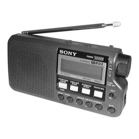
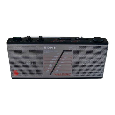
Sony ICF-M1000 User manual

SERVICE MANUAL
FM/AM PLL SYNTHESIZED RADIO
US Model
Canadian Model
AEP Model
UK Model
SPECIFICATIONS
ICF-M1000
Ver. 1.3 2006.10
9-887-063-04
2006J05-1
© 2006.10
Sony Corporation
Personal Audio Division
Published by SonyTechno Create Corporation
Time display
12-hour system (US, Canadian, UK models)
24-hour system (AEP model)
Frequency range
FM : 87.5 - 108 MHz
AM : 530
531 - 1 602 kHz (AEP, UK models)
- 1 710 kHz (US, Canadian models)
Speaker
Approx. 7.7 cm ( 3
1
/
8
inches) dia. 4 Ω
Output
LINE OUT jack (ø 3.5 mm stereo minijack)
i (headphones) jack (ø 3.5 mm stereo minijack)
Input
LINE IN jack (ø 3.5 mm stereo minijack)
Antenna terminal (US, Canadian models)
75 Ωexternal antenna terminal for FM
Power output
4 W (at 10 % harmonic distortion)
Power requirements
120 V AC, 60 Hz (US, Canadian models)
230 V AC, 50 Hz (AEP, UK models)
Dimensions
Approx. 300 ×120 ×170 mm (w/h/d)
(11
7
/
8
×4
3
/
4
×6
3
/
4
inches) not incl. projecting parts and
controls
Mass
Approx.
Approx. 3.0 kg (6 lb 9.83 oz) (AEP, UK models)
2.3 kg (5 lb 1.13 oz) (US, Canadian models)
Supplied accessory
Audio connecting cable (1)
Design and specifications are subject to change without
notice.

2
ICF-M1000
SAFETY-RELATED COMPONENT WARNING!!
COMPONENTS IDENTIFIED BY MARK 0 OR DOTTED LINE
WITH MARK 0ON THE SCHEMATIC DIAGRAMS AND IN
THE PARTS LIST ARE CRITICAL TO SAFE OPERATION.
REPLACE THESE COMPONENTS WITH SONY PARTS WHOSE
PART NUMBERS APPEAR AS SHOWN IN THIS MANUAL OR
IN SUPPLEMENTS PUBLISHED BY SONY.
Notes on chip component replacement
•Never reuse a disconnected chip component.
•Notice that the minus side of a tantalum capacitor may be
damaged by heat.
SAFETY CHECK-OUT
After correcting the original service problem, perform the following
safety check before releasing the set to the customer:
Check the antennaterminals, metal trim, “metallized” knobs,screws,
and all other exposed metal parts forAC leakage.
Check leakage as described below.
LEAKAGE TEST
The AC leakage from any exposed metal part to earth ground and
from all exposed metal parts to any exposed metal part having a
return to chassis, must not exceed 0.5 mA (500 microamperes).
Leakage current can be measured by any one of three methods.
1. A commercial leakage tester, such as the Simpson 229 or RCA
WT-540A. Follow the manufacturers’instructions to use these
instruments.
2. A battery-operatedAC milliammeter. The Data Precision 245
digital multimeter is suitable for this job.
3. Measuring the voltage drop across a resistor by means of a
VOM or battery-operatedAC voltmeter.The “limit” indication
is 0.75V, so analog meters must have an accurate low-voltage
scale. The Simpson 250 and Sanwa SH-63Trd are examples
of a passive VOM that is suitable. Nearly all battery operated
digital multimeters that have a 2VAC range are suitable. (See
Fig. A)
Fig. A. Using an AC voltmeter to check AC leakage.
1.5 k
Ω
0.15
µ
FAC
voltmete
r
(0.75 V)
To Exposed Metal
Parts on Set
Earth Ground
TABLE OF CONTENTS
1. SERVICING NOTES ............................................... 3
2. GENERAL ................................................................... 3
3. DISASSEMBLY
3-1. Disassembly Flow ........................................................... 5
3-2. Panel (Front) Section ....................................................... 5
3-3. Panel (Top) Section, Chassis (Main) Section .................. 6
3-4. MAIN Board, AMPLIFIER Board .................................. 6
4. ELECTRICAL ADJUSTMENTS ......................... 7
5. DIAGRAMS
5-1. Printed Wiring Boards – MAIN/PANEL Section –......... 10
5-2. Schematic Diagram – MAIN/PANEL Section – ............. 11
5-3. Printed Wiring Board – AMPLIFIER Section –.............. 12
5-4. Schematic Diagram – AMPLIFIER Section – ................ 13
5-5. Printed Wiring Boards
– VOLUME/POWER Section – ...................................... 14
5-6. Schematic Diagram – VOLUME/POWER Section –...... 15
6. EXPLODED VIEWS
6-1. Overall Section ................................................................ 17
6-2. Panel (Front) Section ....................................................... 18
6-3. Panel (Top) Section ......................................................... 19
6-4. Chassis (Main) Section.................................................... 20
6-5. Cabinet Section................................................................ 21
7. ELECTRICAL PARTS LIST................................ 22
Ver. 1.1
ATTENTION AU COMPOSANT AYANT RAPPORT
À LA SÉCURITÉ!
LES COMPOSANTS IDENTIFIÉS PAR UNE MARQUE 0SUR
LES DIAGRAMMES SCHÉMATIQUES ET LA LISTE DES
PIÈCES SONT CRITIQUES POUR LA SÉCURITÉ DE
FONCTIONNEMENT. NE REMPLACER CES COM- POSANTS
QUE PAR DES PIÈCES SONY DONT LES NUMÉROS SONT
DONNÉS DANS CE MANUEL OU DANS LES SUPPLÉMENTS
PUBLIÉS PAR SONY.

3
ICF-M1000
SECTION 1
SERVICING NOTES
UNLEADED SOLDER
Boards requiring use of unleaded solder are printed with the lead-
free mark (LF) indicating the solder contains no lead.
(Caution: Some printed circuit boards may not come printed with
the lead free mark due to their particular size)
: LEAD FREE MARK
Unleaded solder has the following characteristics.
•Unleaded solder melts at a temperature about 40 °C higher than
ordinary solder.
Ordinary soldering irons can be used but the iron tip has to be
applied to the solder joint for a slightly longer time.
Soldering irons using a temperature regulator should be set to
about 350 °C.
Caution: The printed pattern (copper foil) may peel away if the
heated tip is applied for too long, so be careful!
•Strong viscosity
Unleaded solder is more viscou-s (sticky, less prone to flow)
than ordinary solder so use caution not to let solder bridges oc-
cur such as on IC pins, etc.
•Usable with ordinary solder
It is best to use only unleaded solder but unleaded solder may
also be added to ordinary solder.
SECTION 2
GENERAL
This section is extracted from
instruction manual.
T
U
N
E
/
T
I
M
E
S
E
T
V
O
L
U
M
E
L
O
W
H
I
G
H
M
I
N
M
A
X
T
O
N
E
BAND/CLOCK RADIO/LINE IN
POWER
FM ANTENNA
LINE OUT LINE IN
EXT INT
i
AM
FM
MHz
kHz
PM
75
AC power cord
FM ANTENNA selector
T
U
N
E
/
T
I
M
E
S
E
T
V
O
L
U
M
E
L
O
W
H
I
G
H
M
I
N
M
A
X
T
O
N
E
BAND/CLOCK RADIO/LINE IN
OPERATE
i
AM
FM
MHz
kHz
PM
LINE IN
AC power cord
Cordon
d’alimentation
secteur
US, Canadian models
AEP, UK models
Ver. 1.3

4
ICF-M1000
Ver. 1.3
Improving the
reception
FM: The AC power cord functions as an FM antenna.
Select FM ANTENNA selector to INT and extend
the AC power cord fully to improve FM reception.
AM: Rotate the unit horizontally for optimum
reception. A ferrite bar antenna is built into the
unit.
Notes
• Do not play the unit over a steel desk or metal surface,
as this may lead to interference of reception.
•If using an external FM antenna, set FM ANTENNA
selector to EXT, then connect the 75 Ωcoaxial cable
(not supplied) to FM ANTENNA (75 Ω)connector on
the rear of the unit.
•To receive FM signals via cable available from some
cable TV providers, contact your cable TV company
for assistance.
Connecting external
equipment
To listen to sound
1
Connect the LINE IN jack of the unit to the
line out jack or headphone jack of the external
equipment using the audio connecting cable
(supplied).
FM ANTENNA
LINE OUT LINE IN
EXT INT
75
Audio connecting cable
(supplied)
To external
equipment
2
Press POWER to turn on the radio.
Setting the clock
1
Plug in the unit.
The display will flash “AM 12:00”.
2
Press POWER to turn off the radio when it
is turned on.
3
Press and hold BAND/CLOCK for a few
seconds.
You will hear a beep and the hour will start to flash
in the display.
4
Turn TUNE/TIME SET right or left until
the correct hour appears in the display.
5
Press BAND/CLOCK once.
The hour is set and the minutes start to flash.
6
Repeat steps 4and 5to set the minute.
Two short beeps sound, “:” starts flashing, and the
clock starts operating.
If you do not set the clock within 65 seconds, the setting
is canceled.
Playing the radio
You can use an external FM antenna although the AC
power cord functions as an FM antenna.
When you use an external FM antenna, connect the
antenna cable to FM ANTENNA connector on the
rear of the radio and then set FM ANTENNA selector
to EXT. When you do not use an external FM antenna,
set FM ANTENNA selector to INT.
1
Press POWER to turn on the radio.
If “LINE” is displayed, press RADIO/LINE IN so
that the frequency appears.
2
Press BAND/CLOCK to select the band
AM or FM.
3
Turn TUNE/TIME SET right or left to
tune in to a desired frequency.
Two short beeps sound when the minimum
frequency of each band is received during tuning.
4
Adjust the volume using VOLUME.
5
Set the tone using TONE.
To adjust the tone, turn TONE to LOW/HIGH.
To listen with the
headphones
You can enjoy the radio and external equipment
connected to the line in by the headphones (not
supplied). Connect the headphones (not supplied)
to the i(headphones) jack. The speaker is
deactivated when the headphones are connected.
The headphones output AM broadcasts in
monaural (same sound is output from both
headphones), while FM stereo broadcasts are
output in stereo.
3
Press RADIO/LINE IN to select “LINE” in
the display.
4
Play the equipment connected to the
LINE IN jack.
5
Adjust the volume using VOLUME.
To return to the radio
Press RADIO/LINE IN.
The frequency is shown in the display.
To record with LINE OUT
1
Connect the LINE OUT jack of the unit to
the line in jack of the external equipment
using the audio connecting cable (supplied).
FM ANTENNA
LINE OUT LINE IN
EXT INT
75
Audio connecting cable
(supplied)
To external
equipment
2
Press POWER to turn on the radio.
3
Tune the unit to the radio station that you
want to record.
4
Start to record on the connected equipment.
Notes
•Refer also to the connected equipment’s manual.
•The supplied audio connecting cable may not be used
with some external equipment. In this case, use a cord
suitable for the external equipment you are using.
•LINE OUT signal of AM broadcasts is output in
monaural (same sound is output from both head-
phones). And LINE OUT signal of FM stereo
broadcasts is output in stereo.
•The sound quality of LINE OUT signal is constant
regardless of the position of TONE, and the output
level is constant regardless of the position of
VOLUME.
• When you listen to the radio with external equipment
connected, turn off the connected equipment because
noise may be caused. If noise continues, even when
the equipment is turned off, disconnect and place the
external equipment away from the unit.
• If there are line out and headphone jacks on external
equipment, connect to the line out jack.
• If you connect with the headphone jack of the external
equipment, some equipment may not perform tone
switch function (e.g., bass boost, equalizer etc.).
Operating the radio
1
Press OPERATE to turn on the radio.
If “LINE” is displayed, press RADIO/LINE IN so
that the frequency appears.
2
Press BAND/CLOCK to select the band
AM or FM.
3
Turn TUNE/TIME SET right or left to
tune in to a desired frequency.
Two short beeps sound when the minimum
frequency of each band is received during tuning.
4
Adjust the volume using VOLUME.
5
Set the tone using TONE.
To adjust the tone, turn TONE to LOW/HIGH.
To listen with the
headphones
You can enjoy the radio and external equipment
connected to the line in by the headphones (not
supplied). Connect the headphones (not supplied)
to the i(headphones) jack. The speaker is
deactivated when the headphones are connected.
The headphones output AM broadcasts in
monaural (same sound is output from both
headphones), while FM stereo broadcasts are
output in stereo.
Improving the
reception
FM: The AC power cord functions as an FM antenna.
Extend the AC power cord fully to increase reception
sensitivity.
AM: Rotate the unit horizontally for optimum reception. A
ferrite bar antenna is built into the unit.
Note
Do not play the unit over a steel desk or metal surface, as this
may lead to interference of reception.
Connecting external
equipment
To listen to sound
1
Connect the LINE IN jack of the unit to the
line out jack or headphone jack of the external
equipment using the audio connecting cable
(supplied).
LINE IN
Audio connecting cable
(supplied)
To external
equipment
2
Press OPERATE to turn on the radio.
3
Press RADIO/LINE IN to select “LINE” in
the display.
4
Play the equipment connected to the
LINE IN jack.
5
Adjust the volume using VOLUME.
To return to the radio
Press RADIO/LINE IN.
The frequency is shown in the display.
Setting the clock
1
Plug in the unit.
The display will flash “AM 12:00” or “0:00”.
2
Press OPERATE to turn off the radio when
it is turned on.
3
Press and hold BAND/CLOCK for a few
seconds.
You will hear a beep and the hour will start to flash
in the display.
The following illustration’s time display is a 24-hour
system.
4
Turn TUNE/TIME SET right or left until
the correct hour appears in the display.
5
Press BAND/CLOCK once.
The hour is set and the minutes start to flash.
6
Repeat steps 4and 5to set the minute.
Two short beeps sound, “:” starts flashing, and the
clock starts operating.
The clock system varies depending on the model
you own.
12-hour system: “AM 12:00” = midnight.
24-hour system: “0:00” = midnight.
If you do not set the clock within 65 seconds, the setting is
cancelled.
To record with LINE OUT
1
Connect the LINE OUT jack of the unit to
the line in jack of the external equipment
using the audio connecting cable (supplied).
LINE IN
Audio connecting cable
(supplied)
To external
equipment
2
Press OPERATE to turn on the radio.
3
Tune the unit to the radio station that you
want to record.
4
Start to record on the connected equipment.
Notes
•Refer also to the connected equipment’s manual.
•The supplied audio connecting cable may not be used with
some external equipment. In this case, use a cord suitable
for the external equipment you are using.
•LINE OUT signal of AM broadcasts is output in monaural
(same sound is output from both headphones). And LINE
OUT signal of FM stereo broadcasts is output in stereo.
•The sound quality of LINE OUT signal is constant
regardless of the position of TONE, and the output level is
constant regardless of the position of VOLUME.
• When you listen to the radio with external equipment
connected, turn off the connected equipment because noise
may be caused. If noise continues, even when the
equipment is turned off, disconnect and place the external
equipment away from the unit.
• If there are line out and headphone jacks on external
equipment, connect to the line out jack.
• If you connect with the headphone jack of the external
equipment, some equipment may not perform tone switch
function (e.g., bass boost, equalizer etc.).
US, Canadian models AEP, UK models
ICF-M1000
5
•This set can be disassembled in the order shown below.
3-1. DISASSEMBLY FLOW
SECTION 3
DISASSEMBLY
Note: Follow the disassembly procedure in the numerical order given.
3-2. PANEL (FRONT) SECTION
SET
3-2. PANEL (FRONT) SECTION
(Page 5)
3-3. PANEL (TOP) SECTION, CHASSIS (MAIN) SECTION
(Page 6)
3-4. MAIN BOARD, AMPLIFIER BOARD
(Page 6)
3
six screws
(R3.1
×
13)
4
screw
(B3)
5
6
flexible flat (11 core) cabl
e
(CN304)
7
panel (front) section
1
three bosses
2
speaker net sub assy
1
three bosses

ICF-M1000
6
3-3. PANEL (TOP) SECTION, CHASSIS (MAIN) SECTION
3-4. MAIN BOARD, AMPLIFIER BOARD
7
cover (jack)
6
three claws
2
panel (top) section
1
flexible flat (20 core) cable
(CN403)
4
connector
(CN305)
3
two screws
(B3)
9
chassis (main) section
8
four screws
(B3)
5
two speaker liad wires
(CN301)
CN301
speaker liad wire
(GRY)
speaker liad wire
(RED)
2
four screws
(B3)
5
four screws
(B3)
6
nut (antenna)
(US, Canadian)
9
lug
8
coaxial (F type) connector
4
MAIN board
1
flexible flat (19 core) cable
(CN2)
q;
flexible flat (19 core) cable
(CN3)
qa
AMPLIFIER board
3
two claws
7
two claws
Ver. 1.2

7
ICF-M1000
AM TRACKING ADJUSTMENT
Adjust for a maximum reading on level meter
T1 450 kHz
( ):AEP, UK models

AM FREQUENCY COVERAGE ADJUSTMENT
Adjustment Part Frequency Display Reading on Digital Voltmeter
L2 530 (531) kHz 2.9 (2.975) ±0.1 (0.025) V
Confirmation 1,710 (1,602) kHz 11.0 (9.5) ±1.5 V
( ):AEP, UK models
AM TRACKING ADJUSTMENT
Adjust for a maximum reading on level meter
L1 580 (621) kHz
CT1 1,490 (1,404) kHz
( ):AEP, UK models
FM FREQUENCY COVERAGE CONFIRMATION
Adjustment Part Frequency Display Reading on Digital Voltmeter
87.5 MHz 2.9 (2.85) ±0.5 (0.15) V
Confirmation 108 MHz 9.0 (10.0) ±2.0 V
FM TRACKING ADJUSTMENT
Adjust for a maximum reading on level meter
L4 87.5 MHz
CT2 108 MHz
Adjustment Location: MAIN board (See page 8)
FM VCO ADJUSTMENT
Setting:
Procedure:
1. Connect the frequency counter to TP9 (MPX), TP8 (RADIO
+B) on the MAIN board, as shown the figure below.
2. Tune the set to 87.5 MHz.
3. Adjust RV1 on the MAIN board for 76 kHz reading on the
frequency counter.
Specified Value: 75.7 to 76.3 kHz
Adjustment Location: MAIN board (See page 8)
SECTION 4
ELECTRICAL ADJUSTMENTS
0 dB=1 µV
[AM]
Setting:
Function : RADIO
Band : AM
[FM]
Setting:
Function : RADIO
Band : FM
•Repeat the procedures in each adjustment several times, and
tracking adjustments should be finally done by the trimmer
capacitors.
AM RF signal
generator
30% amplitude
modulation by
400 Hz signal
Output level: as low as possible
Put the lead-wire
antenna close to
the set.
+
–
level meter
set
4
Ω
MAIN board
headphone jack (J303
)
FM RF signal
generator
22.5 kHz frequency
deviation by 400 Hz
signal
Output level: as low as possible
+
–
level meter
set
4
Ω
0.01
µ
F
MAIN board
TP18 (FM ANTIN)
MAIN board
headphone jack (J303
)
MAIN board
TP2 (RF GND)
digital voltmeter
100 k
Ω
MAIN board
TP1 (VT)
FM RF SSG
Carrier frequency: 87.5 MHz
Modulation: 400 Hz, 30% FM modulation
Output level: 0.1 V (100 dB)
MAIN board
TP18 (FM ANTIN)
0.01
µ
Fset
MAIN board
TP2 (RF GND)
1
µ
F
TP9 (MPX) +
–
frequency counte
r
33 k
Ω
TP8 (RADIO +B)
+
MAIN board
Ver. 1.3

8
ICF-M1000
T1
AM IF Adjustment
L2
AM Frequency
Coverage Adjustment
RV1
FM VCO
Adjustment
AM Tracking Adjustmen
t
CT1
L1
FM Tracking Adjustment L4
CT2
– MAIN Board (Component Side) –
– MAIN Board (Conductor Side) –
TP2
(RF GND)
TP18
(FM ANTIN)
TP8
(RADIO +B)
TP9
(MPX)
TP1
(VT)
Adjustment and Connecting Location:

ICF-M1000
99
ICF-M1000
•A: B+ Line.
•H: adjustment for repair.
•Voltages and waveform are dc with respect to ground
under no-signal (detuned) conditions.
no mark : FM
():AM
[]: LINE
•Voltagesare takenwith aVOM(Input impedance10 MΩ).
Voltage variations may be noted due to normal produc-
tion tolerances.
•Waveform are taken with a oscilloscope.
Voltage variations may be noted due to normal produc-
tion tolerances.
•Circled numbers refer to waveform.
•Signal path.
F: FM (INTERNAL ANTENNA)
L: FM (EXTERNAL ANTENNA)
f: AM
E: LINE IN
j: LINE OUT
•Abbreviation
CND : Canadian model
SECTION 5
DIAGRAMS
•Note for PrintedWiring Boards and Schematic Diagrams
Note on Schematic Diagram:
•All capacitors are in µF unless otherwise noted. (p: pF)
50 WV or less are not indicated except for electrolytics
and tantalums.
•All resistors are in Ωand 1/4W or less unless otherwise
specified.
•f: internal component.
•2: nonflammable resistor.
•C: panel designation.
Note on Printed Wiring Board:
•X: parts extracted from the component side.
•Y: parts extracted from the conductor side.
•W: indicates side identified with part number.
•f: internal component.
•: Pattern from the side which enables seeing.
(The other layers' patterns are not indicated.)
•Circuit Boards Location
•Waveform
– MAIN Board –
1
IC401 wf (XOUT)
500 mV/DIV, 5
µ
s/DIV
13.3
µ
s1.6 Vp-p
VOL board
KEY board
AMPLIFIER boar
d
MAIN board
LCD board
POWER board
Ver. 1.1
Note:
The components identi-
fied by mark 0or dotted
linewith mark 0arecriti-
cal for safety.
Replace only with part
number specified.
Note:
Lescomposants identifiés par
une marque 0sont critiques
pour la sécurité.
Neles remplacer quepar une
pièce portant le numéro
spécifié.

ICF-M1000
1010
ICF-M1000
Q402
BCE
R401
C401
C413 C441
C415
C430
C405
C406
R404 R406
R14
C2
R13
R405
C417
C33
C407
C410
C409
JC402
C402
C403
C404
R425
R426
C431
C432
C434
C433
R427
R428
R429
R430
R431
R432
R433
R437
R415
R447
R446
R438
R408
R409
C439
C446
C438
C420
C418
C442
C443
R419
R416
C422
JC401
JC403
JC409
JC408
JC405
JC404
R434
R435
R436
R403
R402 C421
C412
C411
C419
R443
R417
R30
R11
R22
R15
R17
R23
R12
R16
C23
C43
C24 C22 C19
C13
C17
C42
R18
R21
R20
R10
R29 R25
C45
C44
JC2
C39
TH1
C11
C1
C10
C32
C9
C7
C8
C6
JC1
C5
C4
C12
R5
R2
C27
C26
C28
C25
C36
JC4
JC3
C35
C34
JC406
R24
R31
C436
C447
C448
R407
R442
ECB
Q401
ECB
Q2
C37
C3
R1
R8
R9
R3
R4
Q6
Q5
D4
Q4
BCE
ECB
Q3
ECB
Q1
D5
D3
28
29
42
43
1
56
14
15
IC401
CF4 CF3
CF2
IC1
301
1615
L401
X401
T1 CT2
BPF1
L5
L3
L4
CF1
L2
RV1
CT1
MAIN BOARD
1-869-622- (11, 12)
11, 12
BP401
BP402
R501
R502
D501 D502
LCD401
120
14
LCD BOARD
1-869-626- (11, 12)
11, 12
14
S101 S103 S102
KEY BOARD
1-869-625- (11, 12)
11, 12
JW411
JW401 JW14 JW8
JW9
JW5
JW7
JW6
JW1
JW2
JW11
JW10
JW3
JW410
JW409
JW408
JW407
JW13
JW4
JW15
JW16
JW17
JW402
C20
+
C18
+
C16
+
C15
+
C14
+
C29
+
CN2
1
218
19
CN403
1
2
20
19
TP9
(MPX)
TP1
(VT)
AK
TP18
(FM ANTIN)
TP2
(RF GND)
1
3
TP8
(RADIO +B)
1
3
6
4
2C
1C
2B
E
1B
AMPLIFIER BOARD
CN3
A
(SHIELD)
K
A
AK
A
L1
AM
FERRITE-ROD
ANTENNA
LIQUID CRYSTAL DISPLAY
D501, 502
(LCD BACK LIGHT)
114
BAND/
CLOCK
RADIO/
LINE IN
POWER
W403
A
B
C
D
E
1 2 3 4 5 6 7 8 9 10 11 12
W1
5-1. PRINTED WIRING BOARDS – MAIN/PANEL Section – : Uses unleaded solder.
•See page 9 for Circuit Boards Location.
Ref. No. Location
D3 B-10
D4 C-10
D5 C-10
D501 D-2
D502 D-3
IC1 C-9
IC401 C-7
Q1 C-10
Q2 B-9
Q3 D-8
Q4 D-8
Q5 E-9
Q6 D-8
Q401 B-8
Q402 B-8
(Page 12)
Ver. 1.1
•Semiconductor Location

ICF-M1000
1111
ICF-M1000
C442
C443
R447
C439
C438
R446
R417
R443
C418
C419
C420
JW401
R407
R408
R409 C446
C447
C448
R432
R433
R434
R435
R436
R437
R438
R425
R426
R427
R428
R429
R430
R431
C431
C432
C433
C434
C401
JW409
JW408
R416
R415
C402
C403
R401
X401
JW402
C406
C410
C404
C409
C411
C412
R402
C421
JW1
R405
C25C36
R22
C20
C19
C18
C17
R14
R13
C23
C43
C24
C42
Q401
R15
C22
R17
C45C27R21
R30 R29
C26
R20
R10
R18
C29
C28
JW15
IC1
CN2
JW407
C34
JW17
C39
R442
JW13
R11
R23
RV1
R12
C16
CF1
C15
JW16
R9
JW8
JW6
R8
C4
R2
C3
C2
L4
L3
C14
C13
JW11
D5
R3
C6
C9
C32
C8 C7
C10
C11
JW7 JW9
CN403
R501
R502
TP18 BPF1
CT1
C1
CT2
TP1
C12
C5
JC1
JC2
TH1
TP9
C33
CF4
CF3
CF2
JC3
JC4
TP8
R16
JW4
R31
JW2
C430
C417
Q402
JC409
JC402
L401
220µH
C441
C405
C407
C415R404
C436
R403
C413
IC401
BP402
BP401
C422
R419
JW411
JW410
C44
R24
Q2
Q5
JW3
R25
Q6
JW14
JC408
JC406
JC405
JC403
JC404
C35
Q3
Q4
LCD401
W403
D501
D502
S101
S102
S103
R406
JW5JW10
C37
TP2
R5 R4
R1
T1
JC401
L1
D3
L2
L5
Q1
D4
1
1
4.7k
0.01
0.01
4.7k
100k
100k
0.01
0.01
0.01 10k
10k
10k 100p
100p
100p
47k
47k
47k
47k
47k
47k
47k
47k
47k
47k
47k
47k
47k
47k
220p
220p
220p
220p
0.1
10k
10k
0.01
0.1
47k
75kHz
10p
1
0.1
0.1
1000p
0.01
10k
0.1
10k
10.01
220k
47 16V
1
4.7 50V
0.01
100
2.2k
4700p
2200p
4700p
2200p
2SC4154TP-1EF
10
1
10k
0.04714.7k
100k 100k
1
4.7k
100k
2.2k
4.7
50V
0.47
CXA1238S
19P
4700p
100p
100k
100k
220k
22k
10k
10
50V
2.2 50V
470
10k
1000p
100k
1000p
5p
100 16V
0.01
SVC347S-TL
10k
0.01
220p
1000p
220p 10p
10p
5p
20P
220
220
10p
2p
10p
0
0
100p
0
0
10k
100k
100p
0.01
2SC4154TP-1EF
0
0
1
5p
47p
0.2210k
0.1
10k
470p
-1A7-A
µPD17072GB-578
0.01
47k
0.047
0
RT1N441M-TP-1
RT2N21M-TP
0
RT3AMMM
0
0
0
0
0
4700p
RT1P144M-TP-1
RT1N140M-TP-1
SDPW50H0C0000-JP
SDPW50H0C0000-JP
100k
100p
2.2k 1M
100k
0
HVC202B-TRU
2SC3931-C-TX
HVC202B-TRU
LCD3
LCD4
LCD5
LCD6
LCD7
LCD8
LCD9
LCD0
LCD1
LCD2
LCD3
LCD4
LCD5
LCD6
LCD7
LCD8
LCD9
BAND
POWER
RADIO
BAND
POWER
RADIO
LINE
9V ON
BAND
MUTE1
VT
E-DATA
BEEP
CLOCK
E-DATA
CLOCK
9V ON
MUTE1
LINE
BAND
BEEP
VT
VCOH
VCOL
RON
R ON
BAND
EO
VCOL
VCOH
LCD1
LCD2
COM0
COM1
COM2
COM3
COM0
COM1
COM2
COM3
EO
LCD0
COM0
COM1
COM2
COM3
NC
NC
NC
LCD0
LCD1
LCD2
LCD3
LCD4
LCD5
LCD6
LCD7
LCD8
LCD9
CE
ENCODER-CLOCK
BEEP
ENCODER-DATA
INITIAL IN(1)
INITIAL IN(2)
INITIAL OUT
NC
NC
HP
SP
MUTE2
NC
LINE
BAND/CLOCK
POWER
RADIO/LINE
SP/HP
9V ON
5V ON
TEST MODE
CAP
LCD1
REG
LCD1
CAPLCD0
REGLCD0
REG1
XIN
XOUT
VDD
REG0
GND
MUTE1
BAND
RADIO ON
GND
VCC
BAND
SELECT
AM
IFIN
FM
IFIN
TUNE
IND
ACC/
AFC2
ACC/
AFC1
RIPPLE
FILTER
LCH
OUT
RCH
OUT
ST_IND/
VCOCHECK
PILOTDET
LPF2
PILOTDET
LPF1
PLL
LPF1
REG
AFC
MUTE
VCO
GND
FE OUT
FM/AM
FE GND
RF IN
FM
AM
RF IN
FM RF
FM OSC
AM OSC
FM
DISCRI
MPX
RED
PLL
LPF2
(FM ANTIN)
(RF GND)
FM RF
FM OSC
AM OSC
FM VCO
BUFFER
B.P.F.
(MPX)
AM IFT
BAND SELECT SWITCH
(RADIO B+)
Q401,402
VCOH
VCOL
EO
NC
NC
SYSTEM CONTROLLER
RADIO ON
SWITCH
MUTING
-2
-1
BAND SELECT SWITCH
Q3,4
LIQUID CRYSTAL DISPLAY
D501,502
(LCD BACK LIGHT)
BAND/CLOCK
POWER
RADIO/LINE IN
LOW-PASS FILTER
20
1
41
14
FM/AM FRONT-END,FM/AM DET,MPX
AM FERRITE-ROD
ANTENNA
(VT)
W1
5-2. SCHEMATIC DIAGRAM – MAIN/PANEL Section – •See page 9 forWaveform. •See page 16 for IC Block Diagrams. •See page 16 for IC Pin Function Description.
(Page 13)

ICF-M1000
1212
ICF-M1000
Q308
BCE
R314
C112
C437
C227
C226
C225
C224
C223
C215
R251
R244
R215
R218
C231
C236
C205
C121
C106
C137
C105
C40
C314
C38
C41
C132C232
L302
L301
R28
R26
C136
R320
R115
R116
R154
R113 R305
R108
R213
R103
R107
C102
C202
C307
R106
R27
R155
R153
R142
R102
R202
R203 R208
R104
R205
R206
R207
R304
R204
C221
R216
C237
C206
R117
R118
C131
R256
R217
R143
R149
R243
JC201
R255
R144
C125
C124
C127
C126
C234
C46
C444
C47
R101
R201
R302
C204
C104
R150
C123
C115
C134
R252
R151
R246
R245
R254
R445
R222
R122
C116
C216
C135
C120
C220
C30
C435
C235
R132R134
R309
R308
R233
R257
R221
R121
C212
C308
R133 R232 R234
R135
R236
R235
R307
R311
R310
R260
R237
R240
R137
R239
R238
R259
C233
R261
R159
C133
R157
R136
R313
R141
R315
R242
L303
R158
R139
R140
R418
R412
R241
R138
ECB
Q309
ECB
Q405
ECB
Q404
ECB
Q403
ECB
Q307
ECB
Q205
ECB
Q105
ECB
Q306
ECB
Q204
ECB
Q106
ECB
Q310
ECB
Q301
Q302
BCE
Q206
BCE
Q202
BCE
Q201
BCE
Q102
BCE
Q103
BC
E
Q203
BCE
Q101
BCE
ECB
Q104
ECB
Q7
R211
R212
R210
R209
C111
C211
R105
R111
R112
R258
R124
R110
R109
R156
R123
R125
R224R223
R225
4
1
5
8
IC304
IC303
AMPLIFIER BOARD
81
4
5
IC302
1-869-623- (11, 12)
11, 12
C219
+
C119
+
C309
+
C218
+
C306
+
C117
+
C217
+
C118
+
C305
+
C229
+
C109
+
C129
+
C209
+
C122
+
C222
+
JW333
JW329
JW330
JW331
JW332
JW334
CN301
1
2
CN305
1
1
15
7
JW324
JW317
JW323
JW327
D101
D201
CN303
1
2
11
10
JW311
JW310
JW322
JW312
JW336
JW335
JW313
JW314
JW319
JW303
JW301
JW350
JW307
JW304
JW326
JW318
JW315
JW348
JW337
JW321 JW346
JW349
JW339
JW320
JW316
JW328
JW325
JW340
CN3
1
2
18
19
C301
+
C302
+
C203
+
C103
+
C114
+
C214
+
C310
+
C101
+
C201
+
JW309
JW308
JW341
JW343
JW351
JW342
JW305
JW352
JW302
J301
J302
CN1
D301
JW345
JW344
JW347
JW338
EXT
R
INT
S1
8
5
1
4
IC301
J303
i
PS301
POWER
BOARD
B
VOL BOARD
CN304
C
MAIN BOARD
CN2
A
FM ANTENNA
SELECTOR
LINE IN
LINE OUT
FM ANTENNA
75Ω
A
B
C
D
E
F
1 2 3 4 5 6 7 8 9 10
RED
GRY
GRY
RED
W301 W1
5-3. PRINTED WIRING BOARD – AMPLIFIER Section – : Uses unleaded solder.
•See page 9 for Circuit Boards Location.
(Page 14)
(Page 14) (Page 10)
Ver. 1.1
Ref. No. LocationRef. No. Location
D101 B-4
D201 B-4
D301 E-6
IC301 E-8
IC302 C-7
IC303 D-3
IC304 C-5
Q7 D-9
Q101 D-7
•Semiconductor Location
Ref. No. Location
Q102 D-7
Q103 D-7
Q104 C-7
Q105 C-5
Q106 D-6
Q201 E-7
Q202 E-7
Q203 E-7
Q204 C-6
Q205 C-4
Q206 E-5
Q301 E-6
Q302 E-6
Q306 C-3
Q307 C-4
Q308 D-4
Q309 D-2
Q310 E-5
Q403 D-4
Q404 E-3
Q405 F-2

ICF-M1000
1313
ICF-M1000
R305
R208
R225
R125
R223 R123
L301
R258
R156
L302
C232 C132
C127
C126
R150
C129
R151
R252
C229
R251
C226
C227
C104C204
JW324
CN303
JW327
R122
C122
R222
C109
C209
R257
R132
JW329
JW318
JW328
JW330
R242
L303
R315
R141
JW333
R246
C215 C115
C225R245
C224
C223
R244
JW325
R243JC201
R217
R256
R142
R143
C123R149
C124
C125
R144
JW346
C114
C214
C111
C211
R155
R117
IC302
R221 R121
C212
C112
R157
R159C133C233R261R259
C218
D101D201
C219
JW331
C120C220
R241 R140
C309
C222
JW336
JW332
JW323
R313
R138
R139
C118
C308
R238
R137
C119
C306
C117
R158R136
R240 R239
C217
JW310
C310
R320
R254
JW340
C131
C231R218
R118
C314
JW339
R211
R212
C236
C205 C221
C206
C237
R215
R216
JW320
JW345
C136
C105
C106
C137
C121
R116
R115
JW344
R111
R112
JW343
JW342
R109
C103
R213
JW349
JW338
JW351
R153
JW348
D301
R154 R255
R237
R260C235C135R235R236
C216
C116
R233
R134
R307
R310
C305
R311
R308 R309
R232 R133 R234 R135
R445
C437
R203 R206
Q203
C201
JW309
R207 C202
C102
Q103
R107
C101
R106
JW347
R113
R28
JW341
R27
R26C41
R302
JW337
JW307
C301
JW350
R102
R105
R204 R205
JW352
R202
Q301
JW315 JW316 JW317
JW313
C444
JW312
JW319
JW321
JW335
JW311
JW322
JW326
C30
JW334
R412
C435
CN305
CN3
JW314
JW303JW304
C47
JW305
JW301
C46
R201
R101
JW302
R418
CN1
J301
J302
R224 R124
IC304
IC301
C307
R304
C302
R108
R209 R110
R210
C203
C40
J303
CN301
SP301
C134 C234
Q106
Q206
Q105Q205
Q204Q104
IC303
Q202Q201
Q310
Q306
Q307
C38
Q7
Q302
Q403
R314
Q308
Q309
Q405
Q404
S1
Q102
Q101
JW308
R104
R103
4.7k
10k
47k
47k
22k 22k
1k
1k
1000p 1000p
1000p
470p
10k
4.7
50V
10k
10k
4.7
50V
10k
1000p
470p
0.0220.022
11P
10k
4.7
50V10k
4.7
50V
4.7 50V
2.2k
2.2k
10
4.7k
10
10k
100p 100p
0.022470
470p
1000p
10k
10k 0
47k
100k
10k
10k
0.022
470
470p
1000p
10k
4.7 50V
4.7 50V
0.47
0.47
100k
47k
BA4558F-E2
1k 1k
2.2
2.2
10k
22k0.10.122k10k
100
16V
1SS133T-771SS133T-77
1000
16V
0.010.01
2.2 2.2
10
50V
4.7
50V
1k
4.7k
47k
100 16V
0.01
10k
10k
1000 16V
47
16V
47
16V
220470
4.7k 47k
47
16V
10
50V47k
10k
0.22
0.2222k
22k
100p
470k
22k
0.047
0.047 100p
0.01
0.01
470k
2.2k
0.047
0.047
0.01
0.01
100p
2.2k
470k
470k
22k
470k
4.7 50V
470
10k
1SS133T-77
100k 100k
470
220100p100p47k47k
1
1
10k
10k
1k
100k
10
50V
1k
1k 1k
2.2k 4.7k 100k 100k
2.2k
0.01
1k 10k
2SC4154TP-1EF
4.7 50V
1k 1000p
1000p
2SC4154TP-1EF
1k
4.7
50V10k
470
100k
100
4700.01
100
100
16V
47k
47k
47k 47k
47k
RT1N140M-TP-1
22p
100p 10k
1000p
7P
19P
1
1
47k
47k
100k
2.2k 2.2k
BA4558F-E2
NJM2746RB1
0.1
4.7k
220
10V
10k
470k 2.2k
2.2k
4.7
50V
1000p
2P
2200p 2200p
RT1N140M-TP-1
RT1N140M-TP-1
2SC4154TP-1EF2SC4154TP-1EF
BA5417
2SC4154TP-1EF2SC4154TP-1EF
2SA1602TP-1EF
2SC4154TP-1EF
2SC4154TP-1EF
470p
2SC3931-C-TX
RT1P441M-TP-1
RT1N140M-TP-1
4.7k
2SA1602TP-1EF
2SC4154TP-1EF
RT1N241M-TP-1
RT1P441M-TP-1
2SC4154TP-1EF
2SC4154TP-1EF
47k
1k
NF(R)
RCH IN
LCH IN
NF(L)
FILTER
STBY
POWER
BS(L)
LCH OUT
VCC
RCH OUT
BS(R)
NC
PRE GND2
PRE GND1
GND
FM ANTENNA
75Ω
LINE IN
LINE OUT
LOW-PASS FILTER
LINE AMP
LINE AMP
MUTING
MUTING
BUFFER
(FM ANTENNA SELECTOR)
INT EXT
MUTING
MUTING
MUTINGMUTING
MUTING
MUTINGMUTING
POWER AMP
BUFFER
BUFFER
(FOR RADIO)
(FOR LINE)
Q301,302
RADIO/LINE SELECT SWITCH
MUTING CONTROL
SWITCH
Q404,405
B+ SWITCH
MUTING
MUTING
Q308,403
STANDBY SWITCH
(FOR RADIO)
BUFFER
(FOR LINE)
BUFFER
W1
W301
5-4. SCHEMATIC DIAGRAM – AMPLIFIER Section – •See page 16 for IC Block Diagrams.
(Page
11)
(Page 15) (Page 15)

ICF-M1000
1414
ICF-M1000
C427
C426
D402
C424 C425
C445
C440
C429
C423
JC407
C428
C228
C128
R152
R420
R421
R423
R424
R422
R411
R410
R253
7
1
8
14
IC403
5
18
4
IC402
CN304
SW1
ROTARY ENCODER
TUNE/TIME SET
RV302
VOLUME
RV301
TONE
VOL BOARD
1-869-627- (11, 12)
11, 12
AK
C910
C903
C901
C902
C904
C906
C912
C909
C915
C916
C918
R909
R907
R908
R910
R911
R906
R902
R903
R904
R905
R912
ECB
Q902
ECB
Q901
L902
D913
D909
Q903
T901
R901
L901
IC901
POWER BOARD
1-869-624- (11, 12)
11, 12
C907
+
C911
+
C908
+
C914
+
C913
+
JW902
JW903 JW904
JW901
D902
D904 D905
D901 D903
D906
D910
D912
D911
D907
D908
1
7
C905
+
-2
-1
-2
-1
AMPLIFIER
BOARD
CN303
C
1
2
11
10
NOT REPLACEABLE:
BUILT IN TRANSFORMER
∗
POWER
TRANSFORMER
(AC IN)
1
3
2
AMPLIFIER
BOARD
CN305
B
A
B
C
D
E
F
1 2 3 4 5 6 7 8 9 10
W301
F901
(US)
(CND)
5-5. PRINTED WIRING BOARDS – VOLUME/POWER Section – : Uses unleaded solder.
•See page 9 for Circuit Boards Location.
Ref. No. Location
D402 E-3
D901 B-7
D902 C-7
D903 B-7
D904 C-7
D905 C-8
D906 C-8
D907 C-9
D908 C-9
D909 C-9
D910 D-9
D911 C-9
D912 C-10
D913 D-8
IC402 F-1
IC403 E-2
IC901 D-8
Q901 C-9
Q902 C-9
Q903 C-9
(Page 12)
(Page 12)
Ver. 1.1
•Semiconductor Location

ICF-M1000
1515
ICF-M1000
C128
C228
R253
R152
C440
R424
R423
R422R421
R410
R411
CN304JC407
C425 C424 C423 C445 C427 R420
IC403
D402
JW903
D912 D911
D910
IC901
C916 C915
C913
C912
C911
D909
C910
Q901
Q902
JW902
Q903 R910 R911 D907 R906
R907
D908
R909
C906
JW904
C909R908
C905 C904
D904
D903
C903
C902
D902
D901
L901
L902
JW901
C907
R902
R903
R904
D905
C901
D906
C908
R905
D913
C918
R912
T901
R901
C914
RV302RV301
SW1
C428C429
C426
IC402
100p
100p
2.2k
2.2k
0.47
220k
220k
1M1M
1k
47
11P0
1 0.1 0.1 1 1 220k
TC74VHC14FT
(EKJ)
RB520S-3D
-TE61
1SS133T-77 1SS133T-77
1SS133T-77
XC6201P302PR
0.01 0.01
220
10V 0.01
470
10V
MTZJ-T-77-7.5B
0.01
2SC4154TP
-1EF
2SA1602TP
-1EF
2SC3243
-TP-E
1k 1k 1SS133T-77 10k
4.7k
1SS133T-77
10k
0.01
0.014.7k
4700
16V 0.1
1N4002B
1N4002B
0.1
0.1
1N4002B
1N4002B
10
50V
220
470
470
1SS133T-77
0.1
1SS133T-77
220
25V
10k
MTZJ-T-77-15B
1000p
10k
1M
1/2W
1000
10V
50k/50k50k/50k
220p220p
0.047
TC7W74FU(TE12R)
GND
VCC
CK D Q GND
VCC
CLR
PR Q
POWER
TRANSFORMER
(AC IN)
Q901-903
+7.5V REGULATOR
GIO
+3V REGULATOR
VOLUMETONE
-1 -1-2 -2
ROTARY ENCODER
TUNE/TIME SET
LEVEL SHIFT
DIVIDER
71
∗NOT REPLACEBLE:
BUILT IN TRNASFORMER
W301
F901
(CND)
(US)
3.15A
125V
5-6. SCHEMATIC DIAGRAM – VOLUME/POWER Section – •See page 16 for IC Block Diagrams.
(Page 13)
(Page 13)
Ver. 1.1

ICF-M1000
1616
ICF-M1000
•IC Block Diagrams
– MAIN Board –
IC1 CXA1238S
– VOL Board –
IC402 TC7W74FU
VCO
REGULATOR
FM FRONT-END
AM FRONT-END
MPX
REGULATOR
MONO/STEREO
SELECT
DECORD
AMP
MUTING
AUTO
BLEND
TUNING
INDICATOR
AM IF/
DET
FM IF/
DISCRI
RIPPLE
FILTER
BAND-PASS
MUTE
1
27
28
2930 242526 212223 181920 1617
2 3 4 5 6 7 8 9
PLL LPF1
PILOT DET LPF2
PILOT DET LPF2
ST IND/VCO CHECK
L-CH OUT
VCC
R-CH OUT
RIPPLE FILTER
AGC AFC1
10
AGC AFC2
13
FM IF IN
14
AM IF IN
15
BAND SELECT
11
GND
12
TUNE IND
1/2
COUNTER
1/2
COUNTER
PD1
PD2
FM/AM FE OUT
FM GND
FM RF IN
AM RF IN
FM RF
REG
FM OSC
AFC
AM OSC
MUTE
FM DISCRI
GND
PLL LPF2
MPX REG
VCO
STANDBY
T.S.D.
BS FILTER
PRE GND2
PRE GND1
NF2
IN2
IN1
NF1
FILTER
STBY
POWER GND
BS1
OUT1
VCC
OUT2
103 4 5 6
BS
BS2
2
NC
1 8 97 11 12 13 14 15
+
–
+
–
6
CLR
7
PR
8
VCC
5
Q
RSQ
3
Q
2
D
4
GND
1
CK
QDC
– AMPLIFIER Board –
IC303 BA5417
•IC Pin Function Description
MAIN BOARD IC401 uPD17072GB-578-1A7-A (SYSTEM CONTROLLER)
Pin No. Pin Name I/O Description
1, 2
NC O Not used
3
HP O Connection terminal of external capacitor for headphone
"L": radio off or speaker output, "H": headphone output
4
SP O Connection terminal of external capacitor for speaker
"L": radio off or headphone output, "H": speaker output
5, 6
NC O Not used
7
9V ON O Power amplifier on/off control signal output terminal "H": amplifier on
8
5V ON O Power on/off control signal output terminal Not used
9
LINE O Mode selection signal output terminal "L": radio mode, "H": line mode
10
BAND/CLOCK I BAND/CLOCK key input terminal
11
POWER I POWER key input terminal
12
RADIO/LINE I RADIO/LINE key input terminal
13
TEST MODE I Test mode setting terminal
14 SP/HP I
Speaker/headphone selection signal input terminal "L": headphone, "H": speaker
15
BAND O Band selection signal output terminal "L": FM or line mode, "H": AM
16
MUTE O Muting on/off control signal output terminal "L": muting on
17
RADIO O Radio on/off control signal output terminal "H": radio on
18
GND - Ground terminal
19 EO O
PLL frequency synthesizer charge pump output terminal
20 VCOL I
AM VCO input terminal
21 VCOH I
FM VCO input terminal
22
REG0 O Voltage regulator output terminal for the PLL
23
VDD - Power supply terminal (+3V)
24
XOUT O System clock output terminal (75 kHz)
25
XIN I System clock input terminal (75 kHz)
26
REG1 O Voltage regulator output terminal for the oscillator circuit
27
REGLCD0 - Connection terminal of doubler circuit capacitor for liquid crystal display drive power supply
28
CAPLCD0 - Connection terminal of doubler circuit capacitor
29
CAPLCD1 - Connection terminal of doubler circuit capacitor
30
REGLCD1 - Connection terminal of doubler circuit capacitor for liquid crystal display drive power supply
31 to 34 COM0 to COM3 O
Common drive signal output to the liquid crystal display
35 to 39 NC
ONot used
40 to 49 LCD0 to LCD9 O
Segment drive signal output to the liquid crystal display
50
CE I Power failure detection signal input terminal
51
ENCODER-CLOCK
ISerial data transfer clock signal input from the rotary encoder (TUNE/TIME SET)
52
BEEP O Beep sound output terminal
53
ENCODER-DATA
ISerial data input from the rotary encoder (TUNE/TIME SET)
54, 55
INITIAL IN (1),
INITIAL IN (2) IDestination setting terminal
56
INITIAL OUT O Output terminal for the destination setting

17
ICF-M1000
SECTION 6
EXPLODED VIEWS
Ref. No. Part No. Description Remark Ref. No. Part No. Description Remark
12-664-693-01 RING (TONE) (TONE, HIGH, LOW)
22-664-694-01 RING (TUNE) (VOLUME, MAX, MIN)
32-664-694-11 RING (TUNE) (TUNE/TIME SET)
4X-2108-410-1 NET SUB ASSY, SPEAKER
53-254-145-11 SCREW (B3), (+) BV TAPPING
62-667-344-01 FOOT, RUBBER
72-667-327-01 SHEET (HP JACK), ADHESIVE
82-664-704-01 COVER (HP JACK)
92-667-329-01 CUSHION (PRISM)
10 2-664-709-01 COVER (JACK) (US, CND)
10 2-664-709-11 COVER (JACK) (AEP, UK)
#1 7-621-849-10 SCREW, WOOD +R 3.1X13
6-1. OVERALL SECTION
•Items marked “*” are not stocked since they
are seldom required for routine service. Some
delay should be anticipated when ordering
these items.
•The mechanical parts with no reference
numberin the exploded views are notsupplied.
•Accessories are given in the last of the
electrical parts list.
NOTE:
•-XX and -X mean standardized parts, so they
may have some difference from the original
one.
•Color Indication of Appearance Parts
Example:
KNOB, BALANCE (WHITE) . . . (RED)
↑↑
Parts Color Cabinet's Color
1
#1
#1
panel (front) section
panel (top) section
chassis (main) section
cabinet section
2
3
4
5
5
5
6
67
8
9
10
•Abbreviation
CND: Canadian model
Ver. 1.3
Les composants identifiés par une
marque 0sont critiquens pour la
sécurité.
Ne les remplacer que par une pièce
portant le numéro spécifié.
Thecomponents identifiedby mark
0or dotted line with mark 0are
critical for safety.
Replace only with part number
specified.

18
ICF-M1000
6-2. PANEL (FRONT) SECTION
Ref. No. Part No. Description Remark Ref. No. Part No. Description Remark
51 2-664-692-02 KNOB (TONE)
52 X-2108-785-1 DAMPER (TONE) SUB ASSY
53 3-252-825-11 SCREW (1.7)
54 2-664-691-02 KNOB (VOL)
55 X-2108-783-1 DAMPER (VOL) SUB ASSY
56 2-664-690-02 KNOB (TUNE)
57 X-2108-784-1 DAMPER (TUNE) SUB ASSY
58 2-664-689-01 PANEL (FRONT)
59 2-667-343-01 BUSHING
60 2-667-332-02 CUSHION (COMBINED)
61 A-1169-783-A VOL BOARD, COMPLETE (US, CND)
61 A-1214-705-A VOL BOARD, COMPLETE (AEP, UK)
RV301 1-227-742-11 RES, VAR, CARBON 50K/50K (TONE)
RV302 1-227-742-11 RES, VAR, CARBON 50K/50K (VOLUME)
SW1 1-479-689-11 ENCODER, ROTARY (TUNE/TIME SET)
51
60
supplied with RV301
supplied with RV302
supplied with SW1
RV301
RV302
SW1
52
53
53
53
54
55
56 57
58
59
61
Note: Ref.No. 60 CUSHION (COMBINED) iscombined parts.
Cut out the necessary part to use.
Ver. 1.3

19
ICF-M1000
6-3. PANEL (TOP) SECTION
Ref. No. Part No. Description Remark Ref. No. Part No. Description Remark
101 2-664-710-01 HOLDER (PRISM)
102 3-252-827-01 SCREW (B2.6), (+) BV TAPPING
103 2-664-712-01 PRISM
104 2-631-557-01 CUSHION (SW)
105 X-2108-782-2 PANEL (TOP) SUB ASSY (US, CND)
105 X-2149-706-1 PANEL (TOP) SUB ASSY (AEP, UK)
106 3-246-344-11 FOOT, RUBBER
107 A-1169-778-A LCD BOARD, COMPLETE
108 2-667-341-01 SHIELD (LCD)
109 2-664-707-01 HOLDER (LCD)
LCD401 1-802-095-11 DISPLAY PANEL, LIQUID CRYSTAL
W403 1-832-261-21 CABLE, FLEXIBLE FLAT (20 CORE)
101
not supplied
(KEY board)
LCD board
LCD401
W403
102
102
102
103
104
105
106
106
107
108
109
Ver. 1.3

20
ICF-M1000
6-4. CHASSIS (MAIN) SECTION
Ref. No. Part No. Description Remark Ref. No. Part No. Description Remark
151 A-1169-768-A MAIN BOARD, COMPLETE (US, CND)
151 A-1214-697-A MAIN BOARD, COMPLETE (AEP)
151 A-1215-543-A MAIN BOARD, COMPLETE (UK)
152 2-664-706-01 HOLDER (ANTENNA)
153 2-667-330-01 PLATE (IC), SHIELD
154 3-254-143-11 SCREW (B3), (+) BV TAPPING
155 2-664-703-01 KNOB (ANTENNA) (US, CND)
156 2-667-338-01 NUT (ANTENNA) (US, CND)
157 2-664-701-01 CHASSIS (MAIN)
158 2-667-342-01 LUG (US, CND)
159 A-1169-772-A AMPLIFIER BOARD, COMPLETE (US, CND)
159 A-1214-700-A AMPLIFIER BOARD, COMPLETE (AEP, UK)
160 3-253-143-01 SCREW (B2.6), (+) P TAPPING
CN1 1-817-371-21 CONNECTOR, COAXIAL (F TYPE)
(FM ANTENNA 75Ω) (US, CND)
L1 1-457-234-11 COIL, FERRITE-ROD ANTENNA (MW)
W1 1-832-262-21 CABLE, FLEXIBLE FLAT (19 CORE)
W301 1-832-263-21 CABLE, FLEXIBLE FLAT (11 CORE)
151
not
supplied
AMPLIFIER board
(US, CND)
CN1
L1
W1 W301
MAIN board
152
153
154
154
154
155
156
157
158
159
160
Ver. 1.3
Other manuals for ICF-M1000
4
Table of contents

Other Sony Radio manuals

Sony
Sony ICF-S22 User manual

Sony
Sony ICF-M88B - S2 Sports Bicycle Radio User manual

Sony
Sony XDR-S20 User manual

Sony
Sony ICF-P27 User manual

Sony
Sony ICF-M33RDS User manual

Sony
Sony SRF-46 User manual

Sony
Sony Sports Walkman SRF-H5 User manual

Sony
Sony ICF-SW12 User manual

Sony
Sony ICF-1000L User manual

Sony
Sony SRF-18 User manual

Sony
Sony XDR-S3HD - HD / AM User manual

Sony
Sony ICF-704S User manual

Sony
Sony Walkman SRF-M37 User manual

Sony
Sony Shower Mate ICF-S70 User manual

Sony
Sony SRF-M606 User manual

Sony
Sony ICF-P26 User manual

Sony
Sony XDR-S10HDIP User manual

Sony
Sony ICF-18 User manual

Sony
Sony S2 Sports Walkman SRF-H11 User manual

Sony
Sony ICF-F1 User manual