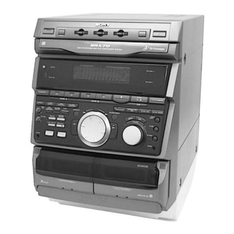
Sony HCD-CP11 User manual

SERVICE
MANUAL
Note
CD
block,
tape
deck
block
and
tuner
pack
are
supplied
with
the
assembled
block.
HCD-CP11
is
the
Amplifier,
CD
player,
Tape
Deck
and
Tuner
section
in
CMT-CP11/CP11K.
HCD-CP11
US
Model
Canadian
Model
AEP
Model
UK
Model
E
Model
Australian
Model
Dolby
noise
reduction
manufactured
under
license
from
Dolby
Laboratories
Licensing
Corporation.
cD
Model
Name
Using
Similar
Mechanism
NEW
“DOLBY”
and
the
double-D
symbol
OO
are
trade-
Section
|
CD
Mechanism
Type
|
_CDMs5-K5BD41
marks
of
Dolby
Laboratories
Licensing
Corporation.
Tape
deck
|
Model
Name
Using
Similar
Mechanism
|
NEW
Section
Tape
Transport
Mechanism
Type
TCB-020
SPECIFICATIONS
Amplifier
section
For
the
U.S.
model
AUDIO
POWER
SPECIFICATIONS
POWER
OUTPUT
AND
TOTAL
HARMONIC
DISTORTION:
With
6-ohm
loads,
both
channels
driven,
from
70
-
20,000
Hz;
rated
18
watts
per
channel
minimum
RMS
power,
with
no
more
than
0.9%
total
harmonic
distortion
from
250
milliwatts
to
rated
output.
North
American
model:
Continuous
RMS
power
output
(reference):
35+35W
(6
ohms
at
1
kHz,
10%
THD)
Total
harmonic
distortion
less
than
0.07%
(6
ohms
at
1
kHz,
18
W)
European
model:
DIN
power
output
(rated):
30+30W
(6
ohms
at
1
kHz,
DIN)
Continuous
RMS
power
output
(reference):
35
+35
W
(6
ohms
at
|
kHz,
10%
THD)
Music
power
output
(reference):
85
+85
W
Other
models:
The
following
measured
at
230
V
AC,
60
Hz
DIN
power
output
(rated):
30+
30
W
(6
ohms
at
|
kHz,
DIN)
Continuous
RMS
power
output
(reference):
35+35W
(6
ohms
at
1
kHz,
10%
THD)
The
following
measured
at
220
V
AC,
60
Hz
DIN
power
output
(rated):
24+
24W
(6
ohms
at
1
kHz,
DIN)
Continuous
RMS
power
output
(reference):
27+27W
(6
ohms
at
1
kHz,
10%
THD)
Inputs
MD
IN
(phono
jacks):
Sensitivity
500
mV,
impedance
47
kilohms
VIDEO
IN
(phono
jacks):
Sensitivity
250
mV,
impedance
47
kilohms
Outputs
LINE
OUT
(phono
jacks):
Sensitivity
250
mV,
impedance
1
kilohm
OPTICAL
DIGITAL
OUT
(CD):
Optical
PHONES
(stereo
phone
jack):
Accepts
headphones
with
an
impedance
of
8
ohms
or
more
SPEAKER:
Active
speaker
system,
6
ohms
—
Continued
on
next
page
—
MICRO
Hi-Fi
COMPONENT
SYSTEM
ON
Y.

CD
player
section
System
Compact
disc
and
digital
audio
system
Laser
Semiconductor
laser
(A
=
780
nm)
Emission
duration:
continuous
Laser
output
MAX
44.6
pW*
General
Power
requirements
North
American
model:
European
model:
Australian
model:
Mexican
model:
120
V
AC,
60
Hz
230
V
AC,
50/60
Hz
220
-
240
V
AC,
50/60
Hz
120
V
AC,
60
Hz
Wavelength
Frequency
response
*
This
output
is
the
value
measured
at
a
distance
of
200
mm
from
the
objective
lens
surface
on
the
optical
pick-up
block
with
7
mm
aperture.
780
-
790
nm
2
Hz
-
20
kHz
(+0.5
dB)
Tape
player
section
Recording
system
4-track
2-channel
stereo
Frequency
response
(DOLBY
NR
OFF)
Tuner
section
50
-
13,000
Hz
(+3
dB),
using
a
Sony
TYPE
I
cassette
50
-
14,000
Hz
(+3
dB),
using
a
Sony
TYPE
II
cassette
FM
stereo,
FM/AM
superheterodyne
tuner
FM
tuner
section
Tuning
range
North
American
model:
Other
models:
Antenna
Antenna
terminals
Intermediate
frequency
AM
tuner
section
Tuning
range
North
American
model:
European
model:
Middle
Eastern
model:
Other
models:
Antenna
Intermediate
frequency
87.5
-
108.0
MHz
(100-kHz
step)
87.5
-
108.0
MHz
(50-kHz
step)
FM
wire
antenna
75
ohm
unbalanced
10.7
MHz
530
-
1,710
kHz
(with
the
tuning
interval
set
at
10
kHz)
531
-
1,710
kHz
(with
the
tuning
interval
set
at
9
kHz)
531
-
1,602
kHz
(with
the
tuning
interval
set
at
9
kHz)
531
-
1,602
kHz
(with
the
tuning
interval
set
at
9
kHz)
530
-
1,710
kHz
(with
the
tuning
interval
set
at
10
kHz)
531
-
1,602
kHz
(with
the
tuning
interval
set
at
9
kHz)
AM
loop
antenna,
external
antenna
terminal
450
kHz
Other
models:
110
-
120
V
or
220
-
240
V
AC,
50/60
Hz
Adjustable
with
voltage
selector
Power
consumption
TOW
Approx.
190
x
252
x
310
mm
incl.
projecting
parts
and
controls
Dimensions
(w/h/d)
Mass
Approx.
5.6
kg
Design
and
specifications
are
subject
to
change
without
notice.

CMT-CP11/CP11K
SERVICE
MANUAL
US
Model
Canadian
Model
AEP
Model
UK
Model
E
Model
¢
CMT-CP11/CP11K
are
composed
of
following
models.
:
As
for
the
service
manual,
it
is
issued
for
each
component
model,
Aus
tr
a
I
an
M
od
el
then,
please
refer
to
them.
CMT-CP11
E
Model
COMPONENT
MODEL
NAME
CMT-CP11K
¢
Abbreviation
CMT-CP11/CP11K
AED
:
North
European
model
SP
_
:
Singapore
model
CND
:
Canadian
model
TH
_
:
Thai
model
COMPACT
DISC
DECK
|
HCD-CP11
TW:
Taiwan
model
KR
_
:
Korea
model
RECEIVER
SYSTEM
EA
_
:
Saudi
Arabia
mode!
MY:
Malaysia
model
SPEAKER
SYSTEM
|
SS-CCP11
AR
_
:
Argentine
model
AUS
:
Australian
model
MX
_:
Mexican
model
HK
__:
Hong
Kong
model
SPECIFICATIONS
PARTS
LIST
General
Part
No.
Description
Remark
Power
requirements
North
American
model:
120
V
AC,
60
Hz
ACCESSORIES
&
PACKING
MATERIALS
European
model:
230
V
AC,
50/60
Hz
286
2
8
2
fe
fe
2
2
fe
fc 2s
eo
oie
eos
2g
2 2
he 2k
oe
2
2
ie
2
2
ok
2
ok
a
Australian
model:
220-240
V
AC,
50/60
Hz
1-418-299-11
COMMANDER,
STANDARD
(RM-SCP1)
Mexican
model:
120
V
AC,
60
Hz
1-501-374-11
ANTENNA,
LOOP
Other
models:
110-120
V
or
220-240V
AC,
1-501-659-61
ANTENNA
(FM){E,
AR,
TW,
KR,
US,
CND,
SP,
MY,
EA,
HK,
TH)
50/60
Hz
1-754-060-11
ANTENNA
(FM){AED,
AEP,
UK,
CIS)
Adjustable
with
voltageselector.
1-569-008-21
ADAPTOR,
CONVERSION
2P
(TW,
SP,
MY,
AUS,
KR,
TH)
Power
consumption
70
W
4-227-681-11
MANUAL,
INSTRUCTION
(ENGLISH)(EXCEPT
AED,
KR,
TH)
4-227-681-21
MANUAL,
INSTRUCTION
(FRENCH)(US,
CND,
EA)
Dimensions
(w/h/d)
Approx.
190
x
252
x
310
mm
incl.
4-227-681-31
MANUAL,
INSTRUCTION
(SPANISH)(AR,
MX)
projecting
parts
and
controls.
4-227-681-41
MANUAL,
INSTRUCTION
(FRENCH,
SPANISH)(AEP,
E,
SP,
MY)
4-227-681-51
MANUAL,
INSTRUCTION
(GERMAN)(AEP)
Mass:
Approx.
5.6
kg
4-227-681-61
MANUAL,
INSTRUCTION
(DUTCH,
ITALIAN,
PORTUGUESE)(AEP}
Supplied
accessories:
Remote
Commander
(1)
4-227-681-71
MANUAL,
INSTRUCTION
(DANISH,
FINNISH,
SWEDISH)(AED)
AM
loop
antenna
(1)
4-227-681-81
MANUAL,
INSTRUCTION
(RUSSIAN,
POLISH)(CIS)
FM
lead
antenna
(1)
4-227-681-91
MANUAL,
INSTRUCTION
(ARABIC)(EA)
Batteries
(2)
4-227-734-11
MANUAL,
INSTRUCTION
(CHINESE)(SP,
MY,
HK,
TW)
4-227-735-31
MANUAL,
INSTRUCTION
(TURKISH){CIS)
Design
and
specifications
are
subject
to
change
without
notice.
4-227-735-41
MANUAL,
INSTRUCTION
(GREEK)(CIS)
4-991-151-01
COVER,
BATTERY
(RM-SCP1)
MICRO
HiFi
COMPONENT
SYSTEM
SON
Y.
2000C001685-1
.
Printed
in
Japan
©2000.3
Sony
Corporation
Published
by
Quality
Assurance
Dept.
9-929-094-11
Home
Audio
Division
Company

TABLE
OF
CONTENTS
1.
SERVICING
NOTES
------:-:ssssecsssecsssseccssseessssseccsssseesssnees
3
9.
GENERAL
sisiciisectdetentipeniacies
pteert
dovact
earns
5
3.
DISASSEMBLY
---------:ssssessssssessoseeccossececsseesesseeesssseecsssevece
7
A.
SERVICE
MODE
-.1-:--s+v--sssssesssosessossesessseessssseccssteesenssenee
11
5.
ELECTRICAL
CONFIRMATIONS
AND
ADJUSTMENTS.
-1-sss-ssssssseesssssseesscssssesscsssseesecsssseesesssssens
12
6.
DIAGRAMS
6-1.
Circuit
Boards
Locations
-escs:ccrrerteeeeeeseeeeeeeeeeeeeaeecsnesenaeees
14
6-2.
Block
Diagram
—
TAPE
Section
—
-++-++++s-sesssseseeeseeeereseeees
15
6-3.
Block
Diagram
—
MAIN
Section
—
--s+ssssssseesssseeeteeeseenne
16
6-4.
Block
Diagram
—
DISPLAY/POWER
SUPPLY
Section
—
--+-+--++1:s-1ee
17
6-5.
Printed
Wiring
Board
-
MAIN
Section
—
--------
18
6-6.
Schematic
Diagram
—
MAIN
Section
(1/2)
—
eres
19
6-7.
Schematic
Diagram
—
MAIN
Section
(2/2)
—
s-+-+ssse
eee
20
6-8.
Printed
Wiring
Boards
—
LCD/HEADPHONE/LOADING/SPEAKER
Section
—-
21
6-9.
Schematic
Diagrams
—
HEADPHONE/SPEAKER
Section
—-:reeeseseceseeeteeeeeers
21
6-10.
Printed
Wiring
Boards
-
CONTROL
Section
—--
ts
6-11.
Schematic
Diagram
-
CONTROL
Section
—
-++-----++--+
23
6-12.
Printed
Wiring
Board
-
POWER
Section
—
-+-++++++:+1+ss+
24
6-13.
Schematic
Diagram
-
POWER
Section
—-----
we
25
6-14.IC
Block
Diagrams
+-++++++++++
seteeeeenesees
26
6-15.IC
Pin
Function
Description
Dee
eceatefascesseVasnadvcdsnnedsasieseasars
28
7.
EXPLODED
VIEWS.
...-------:ccccsccccccecsssreceessecesenteeeseeeene
30
8.
ELECTRICAL
PARTS
LIST
---s--:-:cscscccssecseeseeeeee
34
SECTION
1
SERVICING
NOTES
NOTES
ON
HANDLING
THE
OPTICAL
PICK-UP
|
BLOCK
OR
BASE
UNIT
The
laser
diode
in
the
optical
pick-up
block
may
suffer
electrostatic
break-down
because
of
the
potential
difference
generated
by
the
charged
electrostatic
load,
etc.
on
clothing
and
the
human
body.
During
repair,
pay
attention
to
electrostatic
break-down
and
also
use
the
procedure
in
the
printed
matter
which
is
included
in
the
repair
parts.
The
flexible
board
is
easily
damaged
and
should
be
handled
with
care.
NOTES
ON
LASER
DIODE
EMISSION
CHECK
The
laser
beam
on
this
model
is
concentrated
so
as
to
be
focused
on
the
disc
reflective
surface
by
the
objective
lens
in
the
optical
pick-
up
block.
Therefore,
when
checking
the
laser
diode
emission,
observe
from
more
than
30
cm
away
from
the
objective
lens.
Notes
on
chip
component
replacement
¢
Never
reuse
a
disconnected
chip
component.
¢
Notice
that
the
minus
side
of
a
tantalum
capacitor
may
be
dam-
aged
by
heat.
Flexible
Circuit
Board
Repairing
*
Keep
the
temperature
of
the
soldering
iron
around
270
°C
dur-
ing
repairing.
¢
Do
not
touch
the
soldering
iron
on
the
same
conductor
of
the
circuit
board
(within
3
times).
¢
Be
careful
not
to
apply
force
on
the
conductor
when
soldering
or
unsoldering.
CAUTION
Use
of
controls
or
adjustments
or
performance
of
procedures
other
than
those
specified
herein
may
result
in
hazardous
radiation
exposure.
This
appliance
is
classified
as
a
CLASS
1
LASER
product.
The
CLASS
1
LASER
PRODUCT
MARKING
is
located
on
the
rear
exterior.
CLASS
1
LASER
PRODUCT
LUOKAN
1
LASERLAITE
KLASS
1
LASERAPPARAT
Laser
component
in
this
product
is
capable
of
emitting
radiation
exceeding
the
limit
for
Class
1.
The
following
caution
label
is
located
inside
the
unit.
CAUTION
—:
INVISIBLE
LASER
RADIATION
WHEN
OPEN
AND
INTERLOCKS
DEFEATED.
AVOID
EXPOSURE
TO
BEAM.
ADVARSEL
:
usvNuc
LASERSTRALING
VED
ABNING
NAR
SIKKERHEDSAFBRYOERE
ER
UDE
AF
FUNKTION.
UNDGA
UDSAETTELSE
FOR
STRALING.
VORSICHT
:
uNsicHTBARE
LASERSTRAHLUNG,
WENN
ABDECKUNG
GEOFFNET
UND
SICHERUEITSVERRIEGELUNG
UBERBRUCKT.
NICHT
DEM
STRAHL
AUSSETZEN.
VARO!
}
AVATTAESSA
JA
SUOJALUKITUS
OHITETTAESSA
OLET
ALT-
THNA
NAKYMATTOMALLE
LASERSATEILYLLE.
ALA
KATSO
SATEESEEN.
VARNING
_
:
OSYNUNGLASERSTRALING
OCH
SPARREN
AR
URKOPPLAD.
BETRAKTA
EJ
STRALEN.
NAR
DENNA
DEL
AR
OPPNAD
ADVERSEL
:
usyniic
LASERSTRALING
NAR
DEKSEL
APNES
OG
SIKKERHEDSLAS
BRYTES.
UNNGA
EKSPONERING
FOR
STRALEN.
VIGYAZAT!
:
4
BURKOLAT
NYITASAKOR
LATHATATLAN
LEZERSU-
GARVESZELY/
KEROLJE
A
BESUGARZAST!
SAFETY-RELATED
COMPONENT
WARNING!!!
COMPONENTS
IDENTIFIED
BY
MARK
A
OR
DOTTED
LINE
WITH
MARK
A
ON
THE
SCHEMATIC
DIAGRAMS
AND
IN
THE
PARTS
LIST
ARE
CRITICAL
TO
SAFE
OPERATION.
REPLACE
THESE
COMPONENTS
WITH
SONY
PARTS
WHOSE
PART
NUMBERS
APPEAR
AS
SHOWN
IN
THIS
MANUAL
OR
IN
SUPPLEMENTS
PUBLISHED
BY
SONY.
ATTENTION
AU
COMPOSANT
AYANT
RAPPORT
ALA
SECURITE!
LES
COMPOSANTS
IDENTIFES
PAR
UNE
MARQUE
A
SUR
LES
DIAGRAMMES
SCHEMATIQUES
ET
LA
LISTE
DES
PIECES
SONT
CRITIQUES
POUR
LA
SECURITE
DE
FONCTIONNEMENT.
NE
REMPLACER
CES
COMPOSANTS
QUE
PAR
DES
PIESES
SONY
DONT
LES
NUMEROS
SONT
DONNES
DANS
CE
MANUEL
OU
DANS
LES
SUPPEMENTS
PUBLIES
PAR
SONY.
SAFETY
CHECK-OUT
After
correcting
the
original
service
problem,
perform
the
following
safety
checks
before
releasing
the
set
to
the
customer:
Check
the
antenna
terminals,
metal
trim,
“metallized”
knobs,
screws,
and
all
other
exposed
metal
parts
for
AC
leakage.
Check
leakage
as
described
below.
LEAKAGE
The
AC
leakage
from
any
exposed
metal
part
to
earth
ground
and
from
all
exposed
metal
parts
to
any
exposed
metal
part
having
a
return
to
chassis,
must
not
exceed
0.5
mA
(500
microamperes).
Leakage
current
can
be
measured
by
any
one
of
three
methods.
1.
Acommercial
leakage
tester,
such
as
the
Simpson
229
or
RCA
WT-540A.
Follow
the
manufacturers’
instructions
to
use
these
instruments.
2.
A
battery-operated
AC
milliammeter.
The
Data
Precision
245
digital
multimeter
is
suitable
for
this
job.
3.
Measuring
the
voltage
drop
across
a
resistor
by
means
of
a
VOM
or
battery-operated
AC
voltmeter.
The
“limit”
indication
is
0.75
V,
so
analog
meters
must
have
an
accurate
low-voltage
scale.
The
Simpson
250
and
Sanwa
SH-63Trd
are
examples
of
a
passive
VOM
that
is
suitable.
Nearly
all
battery
operated
digital
multimeters
that
have
a
2V
AC
range
are
suitable.
(See
Fig.
A)
To
Exposed
Metal
Parts
on
Set
AC
/_|
Voltmeter
1.5Q
(0.75)
|
|
0.15
uF
i
ae
L_4+
="
Earth
Ground
Fig.
A.
Using
an
AC
voltmeter
to
check
AC
leakage.
MODEL
IDENTIFICATION
—
Back
Panel
-—
Power
Voltage
Indication
VOLTAGE
SELECTOR
Switch
Power
Voltage
Incdication
AC:
120
V
60
Hz
55
W
AC:
230
V
50
Hz
55
W
AC:
110
—
120/
220
—
240
V
/
50/60
Hz
55
W
Model
+
US,
CND,
MX,
KR
models
AEP,
UK,
AED,
CIS,
models
E,
EA,
AR,
HK,
MY,
SP,
TW,
AUS
models
Abbreviation
EA
—
:
Saudi
Arabia
model.
AUS
__
:
Australian
model.
SP
__:
Singapore
model.
MY
—
:
Malaysia
model.
TW
_
:
Taiwan
model.
HK
—
:
Hong
Kong
model.
AR
_
:
Argentine
model.
CND_:
Canadian
model.
AED:
North
European
model.
MX
—
:
Mexican
model.
KR
—
:
Korean
model.

SECTION
2
GENERAL
LOCATION
OF
CONTROLS
*
Front
View
ICRC
CINE
ECOPOSNES
—
Q
—_ —_
=
in)
[es]
—_
>
=a)
=
3]
[el
|
—=_
~I
—_
fo}
28
29 Bo
BT
¢
Rear
View
o>]
[on]
[a
~)
SRESES&
IN]
{o>} [oy]
[B]
[o9]
[ro]
[]
TAPE
deck
26]
jack
Liquid
crystal
display
27]
PHONES
jack
TAPE
Hf
button
28)
CD
disc
tray
TAPE
<<
button
29)
VOLUME
knob
TAPE
<>
button
30}
CD
Pll
button
TAPE
&
button
31]
CD
Kid
<4
button
TAPE
Mf
button
32}
CD
PLAY
MODE
button
TAPE
button
TAPE
REC
@
button
CD
SYNC
button
and
indicator
BAND
button
TUNING
+
button
TUNING
~
button
TUNING
MODE
button
CD
EJECT
&
button
CD
@
button
CD
Pi
&P
button
CD
REPEAT
button
DSG
button
and
indicator
STANDBY
I/C)
button
and
indicator
MD/VIDEO
button
and
indicator
TAPE
button
and
indicator
CD
button
and
indicator
TUNER
button
and
indicator
Remote
sensor
AM
ANTENNA
terminals
FM
ANTENNA
jack
or
terminals
SPEAKER
terminals
LINE
OUT
jacks
MD
IN
jacks
VIDEO
IN
jacks
CD
DIGITAL
OUT
OPTICAL
connector

Step
2:
Setting
the
time
Before
you
can
use
the
system’s
timer
functions,
set
the
internal
clock.
The
clock
uses
a
24-hour
system
on
the
European
model,
and
a
12-hour
system
on
other
models.
The
24-hour
system
is
used
here
for
illustration
purposes.
1
Press
TIMER
SET.
The
hour
indication
flashes.
2
Press
KKI/DDI
repeatedly
to
set
the
hour.
This
section
is
extracted
from
instruction
manual.
3
Press
ENTER.
The
minute
indication
flashes.
4
Press
KKI/DDI
repeatedly
to
set
the
minute.
5
Press
ENTER.
The
clock
will
begin
operating.
To
reset
the
system
clock
You
can
reset
the
system
clock
even
when
the
system
is
on
or
off.
1
Press
TIMER
SET.
2
Press
KX/DP>I
repeatedly
until
“SET
CLOCK”
appears,
then
press
ENTER.
3
Repeat
step
2
to
5
in
“Step
2:
Setting
the
time”.
Tip
If
you
make
a
mistake,
start
over
from
step
1.

SECTION
3
DISASSEMBLY
Note:
Follow
the
disassembly
procedure
in
the
numerical
order
given.
3-1.
COVER
(UPPER)
©
Cover
(upper)
@
Four
screws
;
Z
(BTP3
x
8)
@
Two
screws
(case3
TP2)
%O—
©
Two
screws
(case3
TP2)
3-2.
TAPE
MECHANISM
DECK
©
Tape
©
Two
screws
mechanism
deck
(BTP3x
8)
@
Connector
@
Fiat
wire
(12
core)
©
Two
screws
(BTP3
x
8)

3-3.
FRONT
PAENL
SECTION
@
Fiat
wire
@
Connector
©
Connector
(CN303)
©
Screw
(TP3
x
6)
Two
claws
©
Screw
(BTP3
x
8)
(KTP3
x
6)
©
Two
screws
@
Front
panel!
section
(There
is
a
claw.)

3-4.CD
MECHANISM
DECK
3-5.
UPPER
CHASSIS

3-6.
TRAY
3
o
®
dK
aN
Aa
WON
the
direction
of
arrow
@
©
Rotate
the
control
cam
in
3-7.
CAM
ey
©
Pull
se
8
@
Roller
@)
é
yy
a
2
=
w
bcs)
10

SECTION
4
SERVICE
MODE
[Liquid Crystal
Display
All
Lit
Check
Mode]
Procedure:
1.
2
3.
4.
Set
to
standby
state.
Press
three
buttons
of
[Ill]
(TAPE),
[ill]
(CD),
and[MD/VIDEO]
simultaneously.
Liquid
crystal
display
are
all
turned
on.
To
exit
from
this
mode,
press
the
button
to
turn
the
power
OFF.
[Tape
Deck
Aging
Mode]
This
mode
can
be
used
for
operation
check
of
tape
deck
section.
Procedure:
1.
Set
a
tape
in
the
tape
deck.
2.
Set
to
standby
state.
3.
Press
three
buttons
of
[Il]
(TAPE),
[Ml]
(CD),
and
simultaneously.
4.
The
aging
is
executed
in
bellow
sequence.
5.
Toexit
from
the
aging
mode,
press
the
|I/
©)
|
button
to
turn
the
power
OFF.
Aging
mode
sequence:
Shut
off
1
minute
REC
pause
for
3
seconds
3
minutes
Fast
forward
Shut
off
1
minute
[
REC
pause
for
3
seconds
|
Shut
off
3
minutes
[CD
Aging
Mode]
This
mode
can
be
used
for
operation
check
of
CD
section.
Procedure:
1.
Load
aCD
disc.
2.
Set
to
standby
state.
3.
Press
three
buttons
of
{il]
(TAPE),
[Ill]
(CD),
and
simultaneously.
4.
The
aging
is
executed
in
bellow
sequence.
5.
Toexit
from
the
aging
mode,
press
the
[1/7
|button
to
turn
the
power
OFF.
Aging
mode
sequence:
Open
the
disc
tray
Close
the
disc
tray
Play
the
last
track
17

SECTION
5
ELECTRICAL
CONFIRMATIONS
AND
ADJUSTMENTS
DECK
SECTION
Note:
Confirm
each
contents
of
this
section
first
of
all.
If
the
results
are
not
satisfied,
do
the
adjustment.
1.
Demagnetize
the
record/playback
head
with
a
head
demagnetizer.
2.
Do
not
use
a
magnetized
screwdriver
for
the
adjustments.
3.
After
the
adjustments,
apply
suitable
locking
compound
to
the
parts
adjust.
4.
The
adjustments
should
be
performed
with
the
rated
power
supply
voltage
unless
otherwise
noted.
5.
The
adjustments
should
be
performed
in
the
order
given
in
this
service
manual.
(As
a
general
rule,
playback
circuit
adjustment
should
be
completed
before
performing
recording
circuit
adjustment.)
6.
The
adjustments
should
be
performed
for
both
L-CH
and
R-
CH.
7.
Switches
and
controls
should
be
set
as
follows
unless
otherwise
specified.
¢
Test
Tape
Tape
P-4-A100
|
10
kHz,
-10
dB
Azimuth
Adjustment
WS-48B
|
3kHz,0dB
P-4-L300
315
Hz,
0
dB
|
Tape
Speed
Adjustment
Level
Adjustment
Record/Playback
Head
Azimuth
Adjustment
Procedure:
1.
Mode:
Playback
test
tape
MAIN
board
P-4-A100
LINE
OUT
jack
(PJ301)
(10
kHz,
-10
dB)
L-CH,
R-CH
level
meter
—_
ia
Cy)
Oo+
—_
12
2.
Turn
the
adjustment
screw
and
check
output
peaks.
If
the
peaks
do
not
match
for
L-CH
and
R-CH,
turn
the
adjustment
screw
so
that
outputs
match
within
1dB
of
peak.
within
n
10B
R-CH
peak
1
Screw
—»
Screw
position
L-CH
R-CH
position
peak
peak
3.
Mode:
Playback
MAIN
board
test
tape
LINE
OUT
jack
(PJ301)
P-4-A100
L-CH
;
oscilloscope
(10
kHz,
-10
dB)
7
waveform
of
oscilloscope
in
phase
45° 90°
135° 180°
good
wrong
=
Repeat
step
1
to
3
in
playback
(REV)
mode.
After
the
adjustments,
apply
suitable
locking
compound
to
the
pats
adjusted.
uM
Adjustment
Location:
reverse

Playback
level
Confirmation
and
Adjustment
Procedure:
Mode:
Playback
test
tape
WS-48B
(3
kHz,
0
dB)
frequency
counter
==
—
=]
eke
MAIN
board
af
LINE
OUT
jack
(PJ301)
L-CH,
R-CH
Confirm
playback
level
is
within
specification
values
as
follows.
If
these
levels
are
out
of
specification
values,
adjust
the
RV151
(L-
CH)
and
RV251
(R-CH)
on
the
MAIN
board
so
that
the
level
meter
reading
become
within
specification
values.
Specification
values:
PJ301
PB
level:
301.5
to
338.3
mV
(-8.2
to
—7.2
dB)
level
difference
between
the
channels:
within
+0.5
dB
Adjustment
Location:
MAIN
board
REC
Bias
Confirmation
and
Adjustment
Procedure:
1.
Mode:
Record
MAIN
board
MD
IN
jack
(P.J301)
L-CH,
R-CH
Bee
+
50
mV
(23.8
dB)
»)
10
kHz
AF
OSC
blank
tape
600Q
CN-123
C2]
stent
co
onal
oo
t'loood
oO
Oo
o
Ld
2.
Mode:
Playback
recorded
portion
bE
MAIN
board
LINE
OUT
jack
(PJ301)
L-CH,
R-CH
level
meter
3.
Confirm
playback
the
signal
recorded
in
step
1
become
specification
values
as
follows.
If
these
values
are
out
of
specification
values,
adjust
the
RV153
(L-CH)
and
RV253
(R-CH)
on
the
MAIN
board
to
repeat
steps
land
2.
Specification
values:
Playback
output
of
315
Hz
to
playback
output
of 10
kHz:
+
0.5
dB
Adjustment
Location:
MAIN
board
REC
Level
Confirmation
and
Adjustment
Procedure:
1.
Mode:
Record
MAIN
board
MD
IN
jack
(PJ301)
L-CH,
R-CH
315
Hz,
50
mV
(-23.8
dB)
AF
OSC
600
Q
attenuator
1
11000
oo
ae
|
blank
tape
CS-123
2.
Mode:
Playback
level
meter
———o
+
MAIN
board
aE
LINE
OUT
jack
(PJ301)
L-CH,
R-CH
3.
Confirm
playback
the
signal
recorded
in
step
1
become
specification
values
as
follows.
If
these
values
are
out
of
specification
values,
adjust
the
RV252
(R-CH)
and
RV152
(L-CH)
on
the
MAIN
board
to
repeat
steps
1
and
2.
Specification
values:
PJ301
PB
level:
47.2
to
53.0
mV
(~
24.3
to
—
23.3
dB)
Adjustment
Location:
MAIN
board
-
MAIN
BOARD
(Conductor
Side)
-
LINE
OUT
(L/R)
PJ301
<
MD
IN
(L/R)
VIDEO
IN
(L/R)
'
'
t
’
‘
1
’
‘
RV252
(R)
REC
Level
RV152
(L)
RV251
(R)
RvV151
(L)
(
Playback
Level
'Q:'O;—
AV253
(R)
ps
caer
RV153
(L)
REC
Bias
13

SECTION
6
DIAGRAMS
NOTE
FOR
PRINTED
WIRING
BOARDS
AND
SCHEMATIC
DIAGARAMS
Note
on
Printed
Wiring
Board:
Note
on
Schematic
Diagram:
*
o———
:
parts
extracted
from
the
component
side.
*
Allcapacitors
are
in
pF
unless
otherwise
noted.
pF:
uF
°
:
parts
extracted
from
the
conductor
side.
50
WV
or
less
are
not
indicated
except
for
electrolytics
:
Pattern
from
the
side
which
enables
seeing.
and
tantalums.
¢
All
resistors
are
in
Q
and
‘/4
W
or
less
unless
otherwise
specified.
*
A
internal
component.
¢
(~~
:
panel
designation.
*
Waveforms
Note:
ee
fer
Ss
“.
The
components
identi-
es
composants
identifiés
par
MAN
Board
fied
by
mark
A\
or
dotted
|
une
marque
A\
sont
critiques:
SSS
ee
ee
line
with
mark
A\
are
criti-
|
pour
la
sécurité.
cal
for
safety.
Ne
les
remplacer
que
par
une
®
IC801
Replace
only
with
part
|
piéce
portant
le
numéro
number
specified.
spécifié.
°
:
B+
Line.
e
:
B-
Line.
4.6Vp-p
¢
[=]
:
adjustment
for
repair.
238ns
*
Voltages
are
taken
with
a
VOM
(Input
impedance
10
MQ).
Voltage
variations
may
be
noted
due
to
normal
produc-
tion
tolerances.
Q)
IC801
@
*
Waveforms
are
taken
with
a
oscilloscope.
Voltage
variations
may
be
noted
due
to
normal
produc-
tion
tolerances.
*
Circled
numbers
refer
to
waveforms.
¢
Signal
path.
“30.5us
5.0Vp-p
>
:TUNER
)
_
:
TAPE
PLAY
))
:
TAPE
RECORD
>
-:CD
PLAY
(ANALOG
OUT)
@)
ics04
@
>
:CD
PLAY
(OPTICAL
OUT)
e
Abbreviation
EA
_
:
Saudi
Arabia
model.
AUS
:
Australian
model.
SP
—_:
Singapore
model.
MY
_
:
Malaysia
model.
peer
4.3Vp-p
TW
__:
Taiwan
model.
HK
—
:
Hong
Kong
model.
AR
_
:
Argentine
model.
CND_
:
Canadian
model.
AED:
North
European
model.
MX
—
:
Mexican
model.
KR
_—
:
Korean
model.
6-1.
CIRCUIT
BOARDS
LOCATION
SPEAKER
board
POWER
board
LCD
board
MAIN
board
HEADPHONE
board
CONTROL
board
LOADING
board
14

6-2.
BLOCK
DIAGRAM
-TAPE
Section
—
PLAYBACK
RV151
PLAYBACK
LEVEL
(L)
L-CH
<=
tp
=>
(RECORD/PLAYBACK)
R-CH
RV253
|
record
|
_\
BIAS
(R)
+
EQ
AMP
1C351
REC-L
KE
eg
2
DECK
PROCESS,
DOLBY
NR
AMP
Y
10352
DECK
A/B
na
SELECT
Lo
DOLBY
NR
=
>>
0
AMP
°
>
>
CIRCUIT
0
REC/PB
REC/PB
sone
oe
|
REC-BIAS
Os5d
of
REC-MUTE
ence
a
RV152
a4
<<
DOLBY
eee
dey
RECORD
|
SS
aa
LEVEL
(L)
o<]
{
L-MUTE
WIT
0351
REC/PB
R-CH
—~A
H
.
Pm
REC/PB
SWITCHING
1C350
o<]
Q355
oC]
4
BIAS
OSC
7351
Y
RECORD
BIAS
(L)
REC
BIAS
SWITCH
Q359,
360
+8V
7150
BIAS
-
KE
TRAP
Kz
AVI53
CAPSTAN/REEL
MOTOR
DRIVE
(CAPSTAN/REEL)
(M)
0657,
659
TRIGGER
PLUNGER
DRIVE
(ERASE)
nS:
e
SIGNAL
PATH
S_>
«TAPE
PLAY
>_»>
:
TAPE
RECORD
1
1
1
1
fl
BIAS
OSC
Q357,
358
(TRIGGER
PLUNGER)
Q656,
658
TAPE
END
DETECT
SENSOR
(1)
TAPE-END
(HEAD
POSITION
DET)
ovo
(HALF
DET
(SIDE-A))
oOo
(HALF
DET
(SIDE-B))
(CASSETTE
IN
DET)
15
15
SYSTEM
CONTROLLER
1¢801
(1/3)
(a)
(Page
16)
(Page
16)
~(C)
(Page
17)
HCD-CP11

HCD-CP11
6-3.
BLOCK
DIAGRAM
-
MAIN
Section
—
(Page
15)
(B)}
"5
=
>
perl
=)
Page
15
Pas
INPUT
SELECT
SWITCH,
va
1
O:
TONE
CONTROL,
won)
i
|
ELECTRICAL
VOLUME
:
'
5)
rr
|
a:
R]!
Q2—
RCH
LINE
AMP
oe
ae
>-+>
=>
1¢307
>
"
€0)
'[L]
Pu301
(2/2)
I
on
fi
x
Hog
LINE
QUT
!
1
SEN
S
MUTING
1
'
—
L]i
Or
=
ato1
RCH
£6)
'[R
a
MUTING
e
vee!
R]:
@4—
a-ch
pot
esk
S
$—~
RCH
es
©
ae
3
vou
=
UME
TONE
CD
ON
5
LOUT
HEADPHONE
R-CH
J301
(Page
17)
0)
-
RCH
Es
CONTROL
}-+}
conTROL
|--{
ATT
6
=>
=~
AMP
=>
R
=
CIRCUIT
CIRCUIT
PHONES
CD
BLOCK
if
sae
1303
ROUT
R-CH
att
CD-L-OUT
22>
a
MUTING
qt
0132
CD-R-OUT
R-CH
OPTICAL
;
MUTING
nae
$301
TRANSCEIVER
|
|
CD
DIGITAL
OUT
oa
12V
CONTROL
SWITCH
;
a
OPTICAL
0313
325,326
POWER
AMP
‘epetaine
-
uly:
USE
60
SDA
CD-DATA
*
a
elas
MUTING
CONTROL
SWITCH
fs
=
0317,
318
t
-
CD-CLK/TU-CLK
0803,
805, 809,
813
+
“"
9823,825,827
Q805
CD
ON
SWITCH
CD-LATCH
’
-
CD-LATCH/TU-CE
—$_$$<————=@
CD-SENSE1
-
+
CD-SENSE1
ae
0813
MD/VIDEO-ON
_
+
aaa
CD-SENSE2
O-—~
+
CD-SENSE2/TU-COUNT
9853
ry
i——+
as
MUTING
anee
80g
VIDEO/MD-MUTE
CONTROL
SWITCH
ss
Ee]
7
CD-SQSO/RDS-DATA
Q303,
304
MD/VIDEO
L____4
0825
¢
-
CD-SQCK/TUNED
AMP-STBY
+
~~
RCH
\____»
—
|
-
CD-SCOR
0827
+-+—
CD-XRST/RDS
ON
sian
|
Sener
t
|
-
HOLD
CD
45V
i
pace:
©-
RDS
ON
TUNER
PACK
stole
ieee
ae
(AEP,
UK,
E)
|
1
SURG
SYSTEM
CONTROLLER
FM_75Q
R-CH a106
1€801
(2/3)
oa
ali
R-CH
&
32.768kH
Lee
ee
ae
OF
Q808
:
e
psi
ween
i
1(US,
Canadian)
I
0824
y
i
aw
X80!
1
fem
|_|
Ms
soMHz
'
1750
Ee
ANT
GND
0806
!
coag
ees
0806,
808,
812,824,826
fend
Q812
TUNER
ON
SWITCH
DISC
TRAY
OPEN/CLOSE
i
=
MOTOR
DRIVE
am]
4
1¢309
0826
Tain
va
TRAY-OPEN
_t
TRAY-CLOSE
AEP
MODEL
M901
SSCS
S
eget
see
Se
se
Sea
eee
hee
eS
:
aie
cad
ie
tania
(
DISC
TRAY
)
e
SIGNAL
PATH
RDS
DECODER
DEES
[>
:
TUNER
1804
EZ>
:
CD
PLAY
(ANALOG
OUT)
O
S—D
(isc
TRAY
CLOSE
DET)
ZZ>>
:
CD
PLAY
(OPTICAL
OUT)
Ss
>.>
_:
TAPE
PLAY
TU
SV
}
>
A
(isc
TRAY
OPEN
DET)
>_>
:
TAPE
RECORD
16
16
16

HCD-CP11
6-4.
BLOCK
DIAGRAM
-
DISPLAY/POWER
SUPPLY
Section
-
(C}
REC/PB
er
er
woes
mE
1¢801
(3/3)
SYSTEM
CONTROLLER
(C801)
B+
eto
RESET
SIGNAL
GENERATOR
1803
-
irr]
om
om
g
[vey
LIQUID
CRYSTAL
2
D815
DISPLAY
1¢
LcD801
2
5
x
Cael
0812 D657
~
660
e
(LCD
BACK
LIGHT)
S
Oo
D81
S
Ble
CASSETTE
HOLDER
BACK
LIGHT
x
0856
(¥)
LED
DRIVE
DSG
0856
D851
STANDBY
N
uc
D867
@)
LED
DRIVE
CD
SYNC
0857
4
x
LED
DRIVE
@)
“0854
D390
0854
TAPE
B+
SWITCH
i
SWITCHING
i.
0858
ee
0390-392
REMOTE
CONTROL
(DISC
TRAY
ILLUMINATION)
D392
RECEIVER
REMOCON
SWITCH
1802
829,830
+N.
;
+75)
FM
7.5V
FM
CIRCUIT
B+
aL
RY
pe
REGULATOR
DRIVE
ig
ne
Go
sine
aR
a
eee
Se
ROTARY
CONTROL
SWITCH
Q323,324
IN
\
RV801
VOLUME
0315,
316
H12V
B+
SWITCH
TDA7439
(IC301)
B+
325,326
I
1
RV802
e
TREBLE
‘4
+9V
LED
DRIVE
¥)
D855
+9
REGULATOR
Q855
TUNER
TUNER
PACK
B+
0313
'
1
REGULATOR
_Ave03_
|
ACODER
CONTROL
SWITCH
BASE
RV803
0321,
322
D307
fi
=
+5V
POWER
TRANSFORMER
=|
a
ne
LED
DRIVE
CD
BLOCK
B+
arora
0852
POWER
AMP
J
8+
=—
RECT
SUB
230V_
REGULATOR
(IC101,
201)
}
p=
D907
-
910
CONTROL
SWITCH
;
=
0311,
312
$801
-
824
+8V
+8V
+12V
CD
BLOCK,
DISC
TRAY
OPEN/
REGULATOR
REGULATOR
CLOSE
MOTOR
DRIVER
(C309)
B+
C311
0301-303
78V
+12V
E
MODEL
+8V
REGULATOR REGULATOR
RECT
10304
0350-351
VOLTAGE
0911-914
SELECTOR
$901
AUDIO
CIRCUIT
-8V
REGULATOR
1¢305
-8V
(E)
RDS
ON
(Page
16)
17
17

HCD-CP11
6-5.
PRINTED
WIRING
BOARD
-
MAIN
Section
—
«See
page
14
for
Circuit
Boards
Location.
a
a
ae
ee
eee
ee
ee
ee
ee
8
1G
TAPE BECK
¢
Semiconductor
Location
[Re.N,
[Location
Ret
Ne.
Lacaion
|
G-6
TO
LC®
BOARD
(Page
21)
=0
TO
LC®
BOARD
(Page
21)
1
~~
aN
1
on
OPTICAL
PIGITAL
OUT
(CB)
TO
C8
BLOCK
G
E
C
D-7
F
G
B
D
1
NOD
OD
TO
:
CONTROL
BOAR®
(Page
22)
ae
ano
TO
(E)
HEASPHONE
BOARD
(Page
21
(F)
TO
LOABING
BOAR®
(Page
21)
nm
t
1
~
1
~
x
POWER
BOARD
(Page
24)
1
~
1
NOD
1
~
Dea
ND
1
for]
MADWEORMVWEOOD
ror)
~
t
lor)
Tv
aS
©
TO
SPEAKER
BOARD
(Page
21)
18
18

6-6.
SCHEMATIC
DIAGRAM
-
MAIN
Section
(1/2)
—
TO
TAPE
BECK
BLOCK
<
=
¢
See
page
35
for
IC
Block
Diagram.
21
22
(MAIN
BOARD
}
(172)
R136
100
1/10w
[=]
Ie
e
(©)
Eee
[Ee
it
4
VE
1
Btow?
&
7.7
#12112
R212
560;
AEP,
UK,
AEB
C1S
CINEboT)
Fv
1K
EXCEPT
ae
=
@)
I.
—wo—l
"TT
(e)|R
0130
47
16¥
R238
10K
1/108
INPUT
SELECT
SWITCH
TONE
CONTROL
ELECTRICAL
IS
70p
SOV
B
&
470
SOV
B
se
cat
cit
#2:R109%,
R209
2.2K:
AEP,
UK.
AEB
CIS
IKs
EXCEPT
3
R303
270
(
—
80L-12v
‘SENSOR-OUT
PLAY-Sw
+12V
R219
#3
RIN
Ik
1/10W
R106
3.3K
1710¥
R102
18x
1/10
3.0
low
||
satin
28.5)
<-28.7>
1
Thy
HEA@PHONE
AMP
POWER
AMP
CNSDS
F301
=>
TO
HEADPHONE
BOARD
=|
@
(PAGE
21)
16303
y
NHB
0.
¥3:R119,
R219
560:AEP,
UK.
AEB.
CIS
+
2K
EXCEPT
*
-20.7
11.4
1.5
10304
KIA7808P_
a
C314
220
16¥
BIS
0.1
25V
B
C317
0.1
25V
B
<20.7>
16505
C316
220
14¥
B301
MTZ-T-77-12B
BtSV
OND
PACK/REC-L/R-
L-IN
LINE.
MUTE.
-8.0
REC/PB
R-IN
8.0 +5V
REO
Tikes
L-OUT
0.1<5.0>.
>
2
.
baad
t
A-GND
So
orht
dex
0<s.
R-OUT
BIAS.
ON/OFF
REC.
MUTE
\_
oLBY.
ON/OFF
C
BOLBY
©
REC-MUTE
O——
REC-BIAS
O
REC/PB
©
LINE-MUTE
©
PACK/REC
©
BY
——-
+12V
0
PLAY
SW
Q—————+
SENSOR-OUT
©
SOL-12V
©
6>
SWITCH
1.41.5)
R321
4.7%
1/10W
TO
SPEAKER
BOARO
#6:R301,
R350
560:EA
HK, MY.
SP,
TW
(PAGE
21)
820:EXCEPT
-22.5V
$1-OND
+22.5V
-12v
($2)
TO
POWER
S28Ne
BOARE
12V62
|
(PAGE
25)
RELAY-ON
CNP30S
Ff
=
=
BS
1
|
f
US.
CNB
AEP,
UK,
|
E,
AEB.
CIS,
HX
AR.
[1310]
A
;
8
|
oS
i
gS
:
FA
g
t
a
i
SWITCHING
'
H
1
US,
CNB. AEP,
UK.
&
AEB
CIS.
MX AR
AUS,
KR
2:
PISC
TRAY
OPEN/CLOSE
MOTOR
ORIVE
©
OPEN
©
CLOSE
TO
(2/2)
O
TRY
SW
-
ya
of
[ly
4
Pee)
ere
LOAD|
3
[pe
a
wz
F299-4.7¢
y
0h
B
ry
4
°
4
Mm
CN306
1€308.
GPIFS2T
3
®
1)
BIN
6)
<2..9>
art
3trx
MUTING
ane
r
=
a
;
#4:
6107,
C207
fot,
0.0082:
EA
HK
MY.
SP.
TW
:
0.012:
US
CNAE
MX
AR
|=
AUS.
KR
z
0.015:
AEP.
UK
AE
cis
|
3
A
i
0.6
(-0
o4
oO
o4
oy
°
a-5V
|O—
TO
CB
BLOCK
ortbtirx
#5:R10S,
R205
3.
3K:AEP,
UK
AE®
CIS
8.
2K:EXCEPT
RiOS
#5
%
C150
4.7
35¥
a8
O-OO-O-O-O-“D-0-O-0)4)5
EE
t
([8_=_=_5_e_2.2.0
“5
ual
=
000000000
eA
a
Sees
REE
BE
<1
©3238
z
pe
BS
De
oe
i
£Eze
——
a)
TO
2/2)
19
19
FM-ON
o-
BUSY
©
avo
P-6NB
12V
0
H/P
CHK
O
B-GNBD
O
GND
CO
BIGITAL
OUT
@
veo
OPTICAL
OPTICAL
TRANSCEIVER
wat
BOARD
HCD-CP11
23
90!
@®ISC
TRAY
CLOSE
9ET)
$902
®ISC
TRAY
OPEN
BET)
M901
BISC
TRAY
OPEN/CLOS!
Table of contents
Other Sony Stereo System manuals

Sony
Sony CMT-DX400A User manual

Sony
Sony ICF-CS20BT User manual

Sony
Sony PMC-DR45 - Personal Component System User manual

Sony
Sony CMT-MX500i User manual

Sony
Sony CMT-EH10 User manual

Sony
Sony MHC-EC69 User manual

Sony
Sony MHC-EC609iP User manual

Sony
Sony CMT-CP11 User manual

Sony
Sony ZS-S10CP User guide

Sony
Sony HCD-DR3 User manual

Sony
Sony MHC-NX1AV User manual

Sony
Sony MHC-GRX990 User manual

Sony
Sony MHC-V90DW User guide

Sony
Sony HCD-A490 User manual

Sony
Sony HCD-RG295 Building instructions

Sony
Sony MHC-G99AV User manual

Sony
Sony MHC-RV55 User manual

Sony
Sony HCD-V909AV User manual

Sony
Sony CMT-G2NIP User manual

Sony
Sony FST-SH2000 User manual