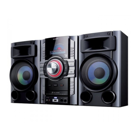
Sony HCD-ED1A User manual

MICROFILM
HCD-ED1A
AEP Model
UK Model
E Model
SERVICE MANUAL
• This service manual and table of repair parts list only the differences with the HCD-ED1.
When performing repairs, refer to both the HCD-ED1 service manual and table of repair parts (9-922-706-XX).
Page HCD-ED1 HCD-ED1A
DIFFERENCE TABLE
62-1. CD DOOR, CD BASE AND BASE UNIT
!¶
Two springs
(compression)
1
Open the CD door.
2
Bar rubber
4
CD player hing
e
6
Hinge pin
5
Hinge spring
3
Screw
(P2x5)
!¡
Three screws (K3x8)
!º
Two hook screws
!™
Three screws (K3x8)
@¡
Base unit
@º
Two springs (compression)
!ª
Two washers
!•
Two screws (TPG P2x8)
!¢
Wire (Flat type)
!∞
Two screws (TPG P2x8)
!§
Two washers
!£
CD base
9
Three screws (K3x8)
7
Two hook screws
8
Three screws (K3x8)
COMPACT DISC DECK RECEIVER
HCD-ED1A

– 2 –
Page HCD-ED1 HCD-ED1A
13
DISPLAY
board
RELAY board
CD DOOR SW
board
BD board
CONTROL BLK ASSY
THIS BLOCK IS SUPPLIED
AS THE ASSEMBLED BLOCK
LED board
DISPLAY
board
CD DOOR SW board
RELAY board
BD board
CONTROL BLK ASSY
THIS BLOCK IS SUPPLIED
AS THE ASSEMBLED BLOCK
LED board
DIFFERENCE TABLE
31
CD DOOR SW BOARD
1
2
D GND
CLOSE SW
M1013 2P
TO
RELAY BOARD
W103
S212
CD DOOR SWITCH
35
1
W104
J211
J210
CD DOOR
210-P125-260
SW PCB
210-P125-270
S212
DOOR SW PCB
TO
RELAY BOARD
W103
CD DOOR SW BOARD
1-671-921-
1-671-922-
(11)
11
(11)
11
HCD-ED1A

– 3 –
• Abbreviation
EE : East European model
HK : Hong Kong model
SP : Singapore model
MY : Malaysia model
NOTE:
• Items marked “*” are not stocked since they are
seldom required for routine service. Some delay
should be anticipated when ordering these items.
Page HCD-ED1 HCD-ED1A
45
***EXPLODED VIEW***
1 4-997-375-01 GLASS DOOR W/PRINGING
3 4-997-355-01 DOOR HINGE
4 4-997-365-01 HINGE PIN
5 4-997-370-01 BAR RUBBER
6 4-997-356-01 HINGE SPRING
7 4-997-349-01 CD BASE
*16 A-4407-244-A CD DOOR SW BOARD, COMPLETE
17 4-977-376-01 STOP SPRING
18 4-977-371-01 STOPPER
NOT USED
Ref. No. Part No. Description Remark
***EXPLODED VIEW***
1 4-214-091-01 GLASS DOOR W/PRINGING
3 4-214-085-01 DOOR HINGE
4 4-214-088-01 HINGE PIN
5 4-214-090-01 BAR RUBBER
6 4-214-086-01 HINGE SPRING
7 4-214-084-01 CD BASE
*16 A-4417-329-A CD DOOR SW BOARD, COMPLETE
17 4-214-956-01 STOP SPRING
18 4-997-371-01 STOPPER
19 4-214-092-01 CD PLAYER HINGE
Ref. No. Part No. Description Remark
1
2
4
5
6
717
9
9
18
10
18
16 19
3
#2
#3
#3
#1
#4 #14
#2
*53 4-214-094-01 REAR PANEL (AEP)
*53 4-214-095-01 REAR PANEL (UK)
*53 4-214-089-01 REAR PANEL (EE,CIS)
*53 4-214-097-01 REAR PANEL (MY,SP)
*53 4-214-096-01 REAR PANEL (HK)
*53 4-997-368-11 REAR PANEL (AEP)
*53 4-997-368-21 REAR PANEL (UK)
*53 4-997-368-31 REAR PANEL (EE,CIS)
*53 4-997-368-51 REAR PANEL (MY,SP)
*53 4-997-368-61 REAR PANEL (HK)
46
111 4-997-357-01 GEAR HOLDER
47 111 4-214-087-01 GEAR HOLDER
***ELECTRICAL PARTS LIST***
*A-4407-244-A CD DOOR SW BOARD, COMPLETE
***************************
S211 1-771-298-11 SWITCH, PUSH (CD DOOR)
51 ***ELECTRICAL PARTS LIST***
*A-4417-329-A CD DOOR SW BOARD, COMPLETE
***************************
S211 1-771-264-11 SWITCH, PUSH (CD DOOR)
***HARDWARE LIST***
NOT USED
58 ***HARDWARE LIST***
#14 7-621-283-00 +P2x5

– 1 –
Model Name Using Similar Mechanism NEW
Base Unit Type BU17-BD19
Optical Pick-up Type KSS-213BA/S-N
Model Name Using Similar Mechanism NEW
TapeTransport MechanismType CMAL2Z076A
SERVICE MANUAL
COMPACT DISC DECK RECEIVER
HCD-ED1 is the tuner, deck, CD and
amplifier section in CMT-ED1.
US Model
Canadian Model
AEP Model
UK Model
E Model
HCD-ED1
— Continued on next page —
This stereo system is equipped with the Dolby* B-
type noise reduction system.
*Dolby noise reduction manufactured under license
from Dolby Laboratories Licensing Corporation.
“DOLBY” and the double-D symbol aare trade-
marks of Dolby Laboratories Licensing Corporation.
CD
SECTION
TAPE
DECK
SECTION
SPECIFICATIONS
9-922-706-12
2001F0200-1
© 2001.6
Sony Corporation
Home Audio Company
Shinagawa Tec Service Manual Production Group

– 2 –
ATTENTION AU COMPOSANT AYANT RAPPORT
À LA SÉCURITÉ!!
LESCOMPOSANTSIDENTIFIÉS PARUNE MARQUE!SUR
LES DIAGRAMMES SCHÉMATIQUES ET LA LISTE DES
PIÈCES SONT CRITIQUES POUR LA SÉCURITÉ DE
FONCTIONNEMENT. NE REMPLACER CES COMPOSANTS
QUE PAR DES PIÈCES SONY DONT LES NUMÉROS
SONT DONNÉS DANS CE MANUEL OU DANS LES
SUPPLÉMENTS PUBLIÉS PAR SONY.
SAFETY CHECK-OUT
After correcting the original service problem, perform the follow-
ing safety checks before releasing the set to the customer:
Checktheantenna terminals, metal trim,“metallized”knobs, screws,
and all other exposed metal parts for AC leakage. Check leakage as
described below.
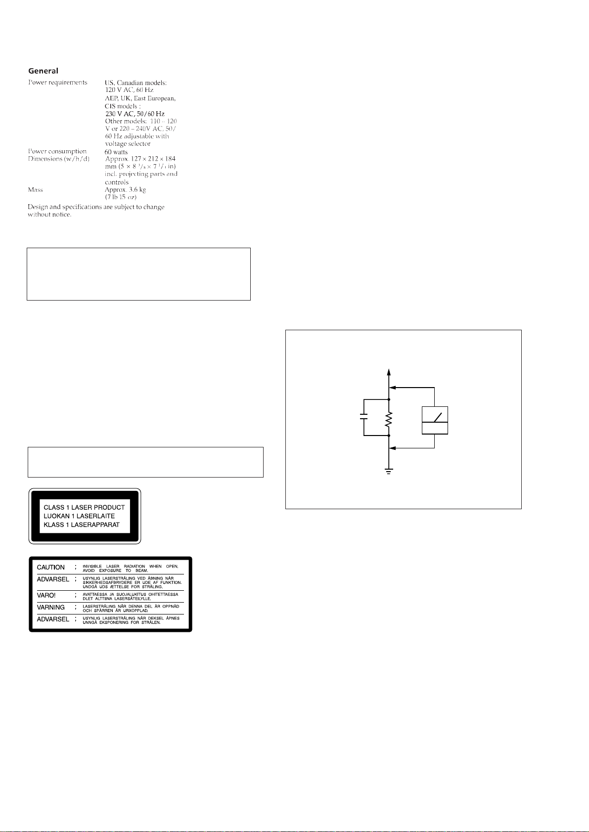
LEAKAGE
The AC leakage from any exposed metal part to earth Ground and
from all exposed metal parts to any exposed metal part having a
returntochassis,mustnotexceed 0.5 mA (500 microampers). Leak-
age current can be measured by any one of three methods.
1. A commercial leakage tester, such as the Simpson 229 or RCA
WT-540A. Follow the manufacturers’ instructions to use these
instruments.
2. A battery-operated AC milliammeter. The Data Precision 245
digital multimeter is suitable for this job.
3. Measuring the voltage drop across a resistor by means of aVOM
or battery-operatedAC voltmeter. The “limit” indication is 0.75
V, so analog meters must have an accurate low-voltage scale.
The Simpson 250 and Sanwa SH-63Trd are examples of a pas-
sive VOM that is suitable. Nearly all battery operated digital
multimeters that have a 2V AC range are suitable. (See Fig. A)
Fig. A. Using an AC voltmeter to check AC leakage.
SAFETY-RELATED COMPONENTWARNING !!
COMPONENTS IDENTIFIED BY MARK!OR DOTTED LINE
WITH MARK !ON THE SCHEMATIC DIAGRAMS AND IN
THE PARTS LIST ARE CRITICAL TO SAFE OPERATION.
REPLACE THESE COMPONENTS WITH SONY PARTS
WHOSE PART NUMBERS APPEAR AS SHOWN IN THIS
MANUAL OR IN SUPPLEMENTS PUBLISHED BY SONY.
Laser component in this product is capable of emitting radiation
exceeding the limit for Class 1.
This appliance is classified as
a CLASS 1 LASER product.
The CLASS 1 LASER PROD-
UCT MARKING is located on
the rear exterior.
This caution
label is located
inside the unit.
CAUTION
Use of controls or adjustments or performance of procedures
other than those specified herein may result in hazardous ra-
diation exposure.
Notes on chip component replacement
• Never reuse a disconnected chip component.
• Notice that the minus side of a tantalum capacitor may be
damaged by heat.
Flexible Circuit Board Repairing
• Keep the temperature of soldering iron around 270˚C
during repairing.
• Do not touch the soldering iron on the same conductor of the
circuit board (within 3 times).
• Be careful not to apply force on the conductor when soldering
or unsoldering.
AC
voltmeter
(0.75V)
1.5k
Ω
0.15
µ
F
Parts on Set
Earth Ground

– 3 –
TABLE OF CONTENTS
1. GENERAL .......................................................................... 4
2. DISASSEMBLY
2-1. CD Door, CD Base and Base Unit ........................................ 6
2-2. Rear Panel ........................................................................... 6
2-3. Bottom Cover and Front Panel Block ................................... 7
2-4. Door CoverAssy and Mechanical Deck (Cassette) .............. 7
3. MECHANICAL ADJUSTMENTS ............................... 8
4. ELECTRICAL ADJUSTMENTS ................................. 8
5. DIAGRAMS
5-1. Circuit Boards Location...................................................... 13
5-2. IC Pin Function ................................................................... 14
5-3. Schematic Diagram — CD Section — ............................... 16
5-4. Printed Wiring Board — CD Section — ............................. 19
5-5. Schematic Diagram — Input/Output Section — ................ 21
5-6. Printed Wiring Board — Input/Output Section — .............. 23
5-7. Printed Wiring Board — Deck Section — .......................... 25
5-8. Schematic Diagram — Deck Section — ............................ 27
5-9. Schematic Diagram — Display Section — ........................ 30
5-10. Printed Wiring Board — Display Section — ...................33
5-11. Schematic Diagram — Power Section — ........................ 36
5-12. Printed Wiring Board — Power Section — ..................... 39
5-13. IC Block Diagrams ........................................................... 41
6. EXPLODED VIEWS
6-1. CD Section ......................................................................... 45
6-2. Rear Panl Section................................................................ 46
6-3. Front Panel Section .............................................................47
6-4. Mechanism Deck Section (Cassette) .................................. 48
6-5. Base Unit Section (BU17-BD19)........................................ 49
7. ELECTRICAL PARTS LIST ........................................ 50
SERVICING NOTE
NOTES ON HANDLINGTHE OPTICAL PICK-UP BLOCK
OR BASE UNIT
The laser diode in the optical pick-up block may suffer electrostatic
break-down because of the potential difference generated by the
charged electrostatic load, etc. on clothing and the human body.
During repair, pay attention to electrostatic break-down and also
use the procedure in the printed matter which is included in the
repair parts.
The flexible board is easily damaged and should be handled with
care.
NOTES ON LASER DIODE EMISSION CHECK
The laser beam on this model is concentrated so as to be focused on
the disc reflective surface by the objective lens in the optical pick-
up block. Therefore, when checking the laser diode emission, ob-
serve from more than 30 cm away from the objective lens.
MODEL IDENTIFICATION
— AC POWER SUPPLY CODE —
AEP, EastEuropean,CISmodel
(Without voltage selector)
Singapore, Malaysia,
Hong Kong model
(With voltage selector)
UK model
US, Canadian model

– 4 –
SECTION 1
GENERAL
120
19
18
17
16
15
14
13
12
2
3
4
5
6
7
8
9
10
11
1
9
8
7
6
5
2
3
4
AEP,UK,
East European
,CIS model
US,Canadian,
Singapore,Malaysia,
Hong Kong model
Location of Parts and Controls
FRONT PANEL
REAR PANEL
1 AMANTENNA
2 MDINjacks
3 MDOUTjacks
4 SPEAKERjacks
5 VOLTAGESELECT ORs witc h
(Malaysia, Singapore ,HongK ongmodelsonl y)
6 FMANTENNAterminal
7 PHONESjack
8 AMANTENNAterminals
9 OPTICALterminal
1 Displa ywindo w
2 DBFBlamp
3 CDSYNClamp
4 REClamp
5ªbutton
6 BANDFM ∏button
7 POWERb utton
8 TUNING ≠º–b utton
9§button(Pushopen)
10 VOLUME–b utton
11 DECKLid
12 VOLUME+b utton
13 TUNING ‚±+button
14 FUNCTONb utton
15 BANDAMπbutton
16 ·button
17 SOUNDMODEb utton
18 WIDElamp
19 Remotesensor
20 NEARF.lamp

– 5 –
This section is extracted from
instruction manual.
REMOTE
1
2
3
4
5
6
7
8
9
10
20
19
18
17
16
15
14
13
12
11
1 DISPLAYbutton
2 DBFBb utton
3 CD b utton
4 TUNER/BANDbutton
5 TAPE œbutton
6 DIRMODEb utton
7 CDREPEA Tbutton
8 b uttons
9 ON/OFFb utton
10 b uttons
11 VOL(+/–)b utton
12 STEREO/MONOb utton
13 TUNING/PLAY MODEb utton
14 DOLBYNRb utton
15 rRECb utton
16 (re wind/fastf orwar d)b uttons
17 AMS*b uttons
18 (stop)b utton
19 (pause)b utton
20 POWERs witc h
*AMS=AutoMusicSensor

– 6 –
SECTION 2
DISASSEMBLY
Note:Follo wthedisassemb lypr ocedureinthen umericalor dergiven.
2-1. CD DOOR, CD BASE AND BASE UNIT
!∞
Two springs
(compression)
1
Open the CD door.
2
Bar rubber
3
Hinge pin
4
Hinge spring
9
Three screws (K3x8)
8
Two hook screws
!º
Three screws (K3x8)
!ª
Base unit
!•
Two springs (compression)
!¶
Two washers
!§
Two screws (TPG P2x8)
!™
Wire (Flat type)
!£
Two screws (TPG P2x8)
!¢
Two washers
!¡
CD base
7
Three screws (K3x8)
5
Two hook screws
6
Three screws (K3x8)
2-2. REAR PANEL
6
Side bracket
7
Rear panel
1
Two screws
(BVTP 3x10)
5
Side bracket
2
Screw
(BVTP 3x8)
3
Two screws
(BVTP 3x8)
4
Three screws
(BVTP 3x8)

– 7 –
2-3. BOTTOM COVER AND FRONT PANEL BLOCK
2-4. DOOR COVER ASSY AND MECHANICAL DECK (CASSETTE)
1
Two screws
(BVTP 3x8)
2
Two screws
(BVTP 3x8)
3
Bottom cove
r
4
Two claws
5
Front panel block
4
Four screws
(BVTP 3x10)
5
Mechanical dec
k
(cassette)
1
Open the Door cover ASSY. (Push the
A
portion.)
2
Door cover assy
3
Door spring
A

– 8 –
SECTION 3
MECHANICAL ADJUSTMENTS
PRECAUTION
1. Clean the following parts with a denatured alcohol-moistened
swab :
record/playback heads pinch rollers
erase head rubber belts
capstan idlers
2. Demagnetize the record/playback head with a head demagne-
tizer.
3. Do not use a magnetized screwdriver for the adjustments.
4. After the adjustments, apply suitable locking compound to the
parts adjusted.
5. The adjustments should be performed with the rated power sup-
ply voltage unless otherwise noted.
Torque Measurement
Torque Torque meter
FWD
Meter reading
FWD
back tension
REV
CQ-102C
CQ-102C
CQ-102RC
CQ-102RC
CQ-201B
CQ-403A
CQ-403R
28 to 71g • cm
(0.39 – 0.99 oz • inch)
1 to 7g • cm
(0.01 – 0.10 oz • inch)
1 to 7g • cm
(0.01 – 0.10 oz • inch)
28 to 71g • cm
(0.39 – 0.99 oz • inch)
DECK SECTION 0 dB=0.775V
1. Demagnetize the record/playbackheadwitha head damagnetizer.
(Do not bring the head demagnetizer close to the erase head.)
2. Do not use a magnetized screwdriver for the adjustments.
3. After the adjustments, apply suitable locking compound to the
parts adjusted.
4. The adjustments should be performed with the rated power sup-
ply voltage unless otherwise noted.
5. The adjustments should be performed in the order given in this
service manual. (As a general rule, playback circuit adjustment
should be completed before performing recording circuit adjust-
ment.)
6. The adjustments should be performed for both L-CH and R-ch.
7. Switches and controls should be set as follows unless otherwise
specified.
SECTION 4
ELECTRICAL ADJUSTMENTS
Tape
P-4-A100
WS-48B
P-4-L300
Signal
10 kHz, –10 dB
3 kHz, 0 dB
315 Hz, 0 dB
Used for
Azimuth Adjustment
Tape Speed Adjustment
Level Adjustment
Record/Playback Head Azimuth Adjustment
Procedure :
1. Mode : Playback
REV
back tension
FF/REW
FWD tension
REV tension 100g or more
(3.53 oz or more)
100g or more
(3.53 oz or more)
56 to 122g • cm
(0.78 – 1.69 oz • inch)
+
–
set
MD OUT (JK301) level meter
test tape
P-4-A100
(10kHz, –10dB)

– 9 –
2. Turn the adjustment screw and check output peaks. If the peaks
do not match for L-CH and R-CH, turn the adjustment screw so
that outputs match within 1 dB of peak.
4. After the adjustments, apply suitable locking compound to the
parts adjusted.
Adjustment Location :
Tape Speed Adjustment
Procedure :
Mode : Playback
3. Mode : Playback
1. Insert the WS-48B into the deck, and playback.
2. Adjust the VR770/RELAY board so that the frequency counter
reading becomes 3000 ± 90 Hz.
Adjustment Location : RELAY board
Sample Value of Wow and flutter
W.RMS (JIS) less than 0.3%
(test tape: WS-48B)
Playback Level Adjustment
Procedure :
Mode : Playback
oscilloscope
MD OUT (JK301)
set
MD OUT (JK301)
test tape
P-4-A100
(10kHz, –10dB)
L
R
Waveform of oscilloscope
good wrong
in phase 45
°
90
°
135
°
180
°
L-CH
peak
R-CH
peak
screw
position
output
level within
1dB
L-CH
peak R-CH
peak
screw
position
within 1dB
+
–
MD OUT (JK301)
set
frequency counte
r
test tape
WS-48B
(3kHz, 0dB)
FWD side REV side
Adjustment screw
level mete
r
MD OUT (JK301)
set
test tape
P-4-L300
(315Hz, 0dB)
Deck is VR703 (L-CH) and VR704 (R-CH)
so that adjustment within the following adjustment level.
Adjustment level :
Playback level: 301.5 to 338.3 mV (–8.2 to –7.2 dB) level dif-
ference between the channels: within ±0.5 dB
Adjustment Location : TAPE PREAMP board

– 10 –
2. Mode : Playback
2. Mode: Playback
Confirm playback the signal recorded in step 1 become adjustment
level as follows.
If these levels do not adjustment level, adjustment the VR701 (L-
CH) and VR702 (R-CH) on the TAPE PREAMP board to repeat
steps 1 and 2.
Adjustment level : Playback output of 10kHz level diffrence
against 315Hz reference should be ±0.5 dB.
Adjustment Location : TAPE PREAMP board
Record Level Adjustment
Procedure :
1. Mode: Record
Confirm playback the signal recorded in step 1 become adjustment
level as follows.
If these levels do not adjustment level, adjustment the VR705 (L-
CH) and VR706 (R-CH) on the TAPE PREAMP board to repeat
steps 1 and 2.
Adjustment level :
Playback level : 47.2 to 53.0 mV (–24.3 to –23.3 dB)
Adjustment Location : TAPE PREAMP board
Adjustment Location
[RELAY BOARD] (Component Side)
Record Bias Adjustment
Procedure :
1. Mode : Record
level mete
r
MD OUT (JK301)
set
recorded
position
AF OSC
attenuator 600
Ω
set
MD IN (JK301)
1) 315Hz
2) 10kHz
blank tape
CS-123
50 mV (–23.8 dB)
}
AF OSC
attenuator 600
Ω
set
MD IN (JK301)
315Hz 50 mV (–23.8 dB)
blank tape
CS-123
VR770
level mete
r
MD OUT (JK301)
set
recorded
position
VR704 VR703 VR706
VR705
VR701
VR702
IC703
121
22
42
[TAPE PREAMP BOARD] (Component Side)

– 11 –
Procedure:
1. Connect oscilloscope to test point TP (RF).
2. Turned Power switch on.
3. Put disc (YEDS-18) in and playback.
4. Adjust RV101 so that the waveform is clear.
(Clear RF signal waveform means that the shape “◊” can be
clearly distinguished at the center of the waveform.)
5. After adjustment, check the RF signal level.
• RF signal
VOLT/DIV: 200 mV
TIME/DIV: 500 nS
S Curve Check
Procedure :
1. Connect oscilloscope to test point TP (FEO).
2. Connect between test pointTP (FOK) and Ground by lead wire.
3. Turn Power switch on.
4. Put disc (YEDS-18) in and turned Power switch on again and
actuate the focus search. (actuate the focus search when disc
table is moving in and out.)
5. Check the oscilloscope waveform (S-curve) is symmetrical be-
tweenA and B.And confirm peak to peak level within 2.4 ± 0.7
Vp-p.
S-curve waveform
6. After check, remove the lead wire connected in step 2.
Note: • Try to measure several times to make sure than the ratio of
A : B or B : A is more than 10 : 7.
• Take sweep timeaslongaspossible and light up the bright-
ness to obtain best waveform.
RF Level Check
Procedure :
1. Connect oscilloscope to test point TP (RF) on BD board.
2. Turned Power switch on.
3. Put disc (YEDS-18) in and playback.
4. Confirm that oscilloscope waveform is clear and check RF sig-
nal level is correct or not.
Note: Clear RF signal waveform means that the shape “◊” can be
clearly distinguished at the center of the waveform.
RF signal waveform
CD SECTION
Note:
1. CD Block is basically designed to operate without adjustment.
Therefore, check each item in order given.
2. UseYEDS-18 disc (3-702-101-01) unless otherwise indicated.
3. Use an oscilloscope with more than 10MΩimpedance.
4. Clean the object lens by an applicator with lens cleaning liquid
when the signal level is low than specified value with the fol-
lowing checks.
5. Adjust the focus bias adjustment when optical block is replaced.
Focus Bias Adjustment
–
+
oscilloscope
BD board
TP (RF)
TP (VC)
level : 1.3
±
0.3 Vp-p
–
+
oscilloscope
BD board
TP (FEO)
TP (VC)
symmetry
A
B
within 2.4
±
0.7 Vp-p
–
+
oscilloscope
BD board
TP (RF)
TP (VC)
level : 1.3
±
0.3 Vp-p
VOLT/DIV : 200 mV
TIME/DIV : 500 nS

– 12 –
Procedure :
1. Connect oscilloscpe to test point TP (TE) on BD board.
2. Turn Power switch on.
3. Put disc (YEDS-18) in to play the number five track.
4. Press the “P(Pause)” button. (Becomes the 1 track jump mode)
5. Confirm that the oscilloscope waveform is symmetrical on the
top and bottom in relation to 0Vdc, and check this level.
1 track jump waveform
E-F Balance (1Track Jump) Check
(Without remote commander)
Specified level: • x 100 = less than ± 7%
• A + B = 300 ± 100 mVp-p
6. Remove the lead wire connected in step 1.
Focus/Tracking Gain Adjustment (RV102, RV103)
This gain has a margin, so even if it is slightly off.
There is no problem.
Therfore, do not perform this adjustment.
Please note that it should be fixed to mechanical center position
when you moved and do not know original position.
A – B
2 (A + B)
Adjustment Location:
[BD BOARD] — Component Side —
–
+
oscilloscope
BD board
TP (TE)
TP (VC)
A
B
0
V
LEVEL : 300
±
100 mVp-p
RF
RV101
RV103
TEO
VC
FEO
RV102
TEI
FEI
FOK
IC101
IC104
GND
PCK
IC102

– 13 –
SECTION 5
DIAGRAMS
5-1. CIRCUIT BOARDS LOCATION
FUN/SURROUND boar
d
VOL/POWER board
TAPE PREAMP board
BD board
CD DOOR SW board
RELAY board
CONTROL BLK ASSY
THIS BLOCK IS SUPPLIED
AS THE ASSEMBLED BLOCK
DISPLAY board
FM/AM TUNER
THIS BLOCK IS SUPPLIED
AS THE ASSEMBLED BLOCK

– 14 –
1
2
3
4
5
6
7
8
9
10
11
12
13
14
15
16
17
18
19
20
21
22
23
24
25
26
27
28
29
30
31
32
33
34
35
36
37
38
39
40
41
42
43
44
45
46
47
48
49
50
GND
XOUT
XIN
RESET
TUNED
STEREO
TEST
POWDEC
REMOTE
PLL CE
PLL CLK
PLL DATAI
PLL DATAO
SERVO CK
SUB Q
DATA
MUTE D
CDPOWER
CLOSESW
FSW
SENSE
MLAT
XLAT
XRST
SCOR
PLAYSW
MTRSNS
TAPEIN
MOTOR
SOL
AMS
PLYMUTE
REC/PB
DOLBYNR
RECMUTE
BIAS
REC LED
CD SYNC
WIDE
KEYIO 1
KEYIO 2
BANDAREA
N.C
LOUDSEL
N.C
FRECSW
RRECSW
AREF
AGND
GND
—
O
I
I
I
I
I
I
I
O
O
I
O
O
I
O
O
O
I
O
I
O
O
O
I
I
I
I
O
O
I
O
O
O
O
O
O
O
O
I
I
—
—
I
—
I
I
I
I
—
Ground
8 MHz Oscillator output
8 MHz Oscillator input
CPU reset input
Station detector input
Stereo signal input
Test pin (Connected to ground)
Power down detect input
Remote signal input
Chip enable output
Clock output
Data input
Data output
Servo clock output
Servo subq data & status input
Servo command data output
Digital mute control output
CD power supply output
Top loading close switch input
Servo focus down output
Servo status SENSE input
D/A MLAT output
Servo command latch output
Servo chip reset output
Servo SUBQ sync input
Tape play switch input
Tape motor reel sense input
Tape in switch input
Tape control output
Tape control output
Tape music search input
Tape play back mute signal output
Tape control output
Tape control output
Tape recording mute signal output
Tape control output
Record LED output
CD SYNC LED output
Wide LED output
AD key input (16 keys)
Band area option (Not used)
Not used
Loudness initial select input
Not used
Tape forward record switch input
Tape reverse record switch input
A/D convert refrence input (+5V)
A/D convert Input ground input
Ground
Pin No. Pin Name I/O Function
5-2. IC PIN FUNCTION
• IC201 MASTER CONTROL (TC9613)

– 15 –
VDD
NARROW
NORMAL
LOUD
DBFB
VOL CLK
VOL DATA
VOL STB
FUNCA
FUNC B
MDMUTE
POWER
MUTEA
SEG27-SEG0
COM3
COM2
COM1
COM0
VLC
N.C
N.C
N.C
VDD
51
52
53
54
55
56
57
58
59
60
61
62
63
64-91
92
93
94
95
96
97
98
99
100
—
O
O
O
—
O
O
O
O
O
O
O
O
O
O
O
O
O
O
—
—
—
—
+5V power supply
Narrow LED output
Normal LED output
Loudness on/off control output
Not used (Connected to ground)
Volume control clock output
Volume control data output
Volume control strobe output
TAPE/TUNER control signal output (00: TAPE/01: TUNER)
CD/MD control signal output (10: CD/11: MD)
MD/REC ON mute output
System power output
Audio mute control output
LCD segment output
LCD common 3 output
LCD common 2 output
LCD common 1 output
LCD common 0 output
LCD drive power supply output
Not used (Connected to ground)
+5V power supply
Pin No. Pin Name I/O Function


This manual suits for next models
1
Table of contents
Other Sony Stereo System manuals

Sony
Sony MHC-C55 User manual

Sony
Sony HCD-HP8V User manual

Sony
Sony HCD-GN1100D User manual

Sony
Sony CMT-CP555 User manual

Sony
Sony HCD-M70 User manual

Sony
Sony HCD-GN100D User manual

Sony
Sony MEX-N4280BT User manual

Sony
Sony LBT-D109CD User manual

Sony
Sony RDP-XF300iPN User manual

Sony
Sony CMT-G1iP User manual

Sony
Sony HCD-EP414 User manual

Sony
Sony FST-GTK11iP User manual

Sony
Sony CMT-MX700Ni User manual

Sony
Sony MHC-V41D User manual

Sony
Sony MHC-EC70 - Mini Hi-fi Component System User manual

Sony
Sony MHC-EC909iP User manual

Sony
Sony CMT-SPZ90DB User manual

Sony
Sony Muteki XROSSFADE LBT-DJ2i User manual

Sony
Sony BKSR-2020 User manual

Sony
Sony HCD-GX8000 User manual