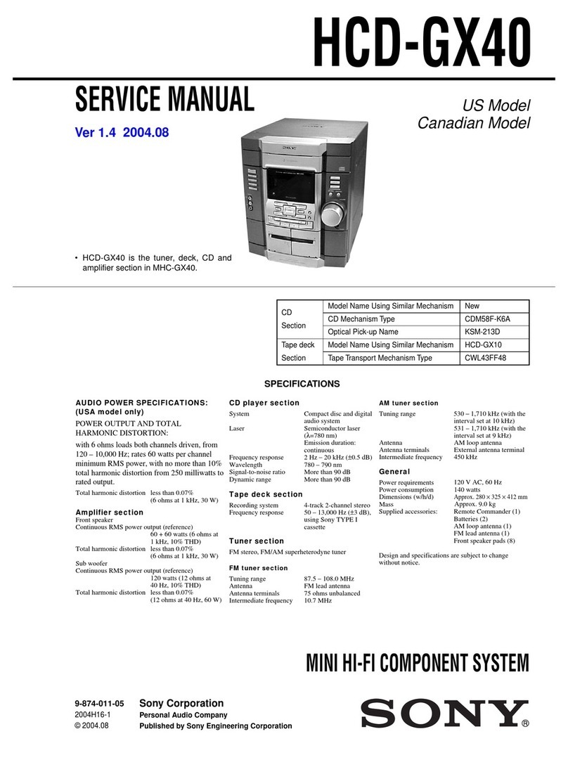
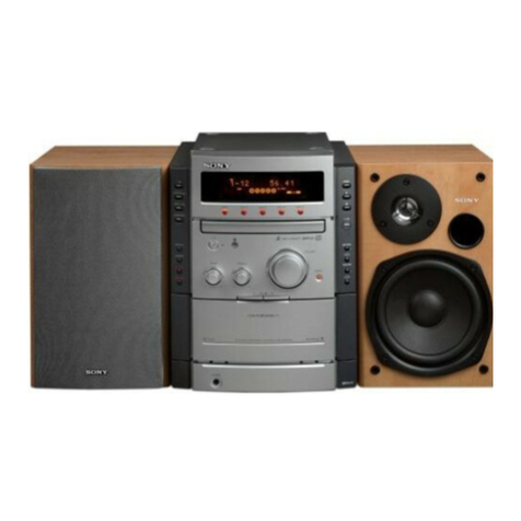
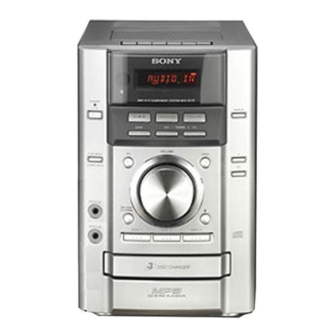
Sony HCD-ED2 - Compact Disc Deck Receiver User manual

1
HCD-ED2
US Model
Canadian Model
AEP Model
UK Model
E Model
Australian Model
SPECIFICATIONS
COMPACT DISC DECK RECEIVER
— Continued on next page —
Model Name Using Similar Mechanism NEW
Mechanism Type CDM-61
Base Unit Type KSM-331AAN/K1NP
Optical Pick-up Type KSS-331A (RP)
Model Name Using Similar Mechanism NEW
Tape Transport Mechanism Type CMAL1Z025A
CD
SECTION
TAPE DECK
SECTION
SERVICE MANUAL
HCD-ED2 is the tuner, deck, CD and
amplifier section in CMT-ED2.
Ver 1.2 2004.05
With CORRECTION-1R
(9-929-025-92)
9-929-025-13
2004E02-1
© 2004.05
Sony Corporation
Home Audio Company
Published by Sony Engineering Corporation
This systems is equipped with the Dolby* B-type noise
reduction system.
*Dolby noise reduction manufactured under license
from Dolby Laboratories Licensing Corporation.
“DOLBY” and the double-D symbol aare
trademarks of Dolby Laboratories Licensing
Corporation.
Amplifier section
For the U.S. model
AUDIO POWER SPECIFICATIONS
POWER OUTPUT AND TOTAL HARMONIC
DISTORTION:
With 8-ohm loads both channels driven from
90 - 15,000 Hz; rated 15 watts per channel
minimum RMS power with no more than 09.%
total harmonic distortion from 250 milliwatts to
rated output.
North American model:
Continuous RMS power output (reference):
17 + 17 W
(8 ohms at 1 kHz, 10%THD)
European model:
DIN power output (rated):
15 + 15 W
(8 ohms at 1 kHz, DIN)
Continuous RMS power output (reference):
17 + 17 W
(8 ohms at 1 kHz, 10% THD)
Music power output (reference):
35 + 35 W
Other models:
The following measured at 230 V AC, 60 Hz
DIN power output (rated):
15 + 15 W
(8 ohms at 1 kHz, DIN)
Continuous RMS power output (reference):
17 + 17 W
(8 ohms at 1 kHz, 10%THD)
Inputs
MD IN (phono jacks) :
Sensitivity 1,000 mV, impedance
47 kilohm
CD DIGITAL OUT OPTICAL:
optical
PHONES (stereo phone jack):
Accepts headphones with an
impedance of 8 ohms or more
SPEAKER: Accepts Impedance of 8 to 16
ohms
CD player section
System Compact disc and digital
audio system
Laser Semiconductor laser
(λ= 780 nm)
Emission duration: continuous
Laser output MAX 44.6 µW*
*This output is the value
measured at a distance of
200 mm from the
objective lens surface on
the Optical Pick-up Block
with 7 mm aperture.
Wavelength 780 - 790 nm
Frequency response2 Hz - 20 kHz (±0.5 dB)
Tape player section
Recording system 4-track 2-channel stereo
Frequency response (DOLBY NR OFF)
50 - 13,000 Hz (±3 dB),
using a Sony TYPE I cassette
50 - 14,000 Hz (±3 dB),
using a Sony TYPE II cassette

2
SAFETY-RELATED COMPONENT WARNING !!
COMPONENTS IDENTIFIED BY MARK !OR DOTTED LINE
WITH MARK !ON THE SCHEMATIC DIAGRAMS AND IN
THE PARTS LIST ARE CRITICAL TO SAFE OPERATION.
REPLACE THESE COMPONENTS WITH SONY PARTS
WHOSE PART NUMBERS APPEAR AS SHOWN IN THIS
MANUAL OR IN SUPPLEMENTS PUBLISHED BY SONY.
CAUTION
Use of controls or adjustments or performance of procedures
other than those specified herein may result in hazardous ra-
diation exposure.
Notes on chip component replacement
• Never reuse a disconnected chip component.
• Notice that the minus side of a tantalum capacitor may be
damaged by heat.
Flexible Circuit Board Repairing
• Keep the temperature of soldering iron around 270˚C
during repairing.
• Do not touch the soldering iron on the same conductor of the
circuit board (within 3 times).
• Be careful not to apply force on the conductor when soldering
or unsoldering.
Laser component in this product is capable of emitting radiation
exceeding the limit for Class 1.
This appliance is classified as
a CLASS 1 LASER product.
The CLASS 1 LASER PROD-
UCT MARKING is located on
the rear exterior.
This caution
label is located
inside the unit.
ATTENTION AU COMPOSANT AYANT RAPPORT
À LA SÉCURITÉ!!
LES COMPOSANTS IDENTIFIÉS PAR UNEMARQUE !SUR
LES DIAGRAMMES SCHÉMATIQUES ET LA LISTE DES
PIÈCES SONT CRITIQUES POUR LA SÉCURITÉ DE
FONCTIONNEMENT.NEREMPLACERCES COMPOSANTS
QUE PAR DES PIÈCES SONY DONT LES NUMÉROS
SONT DONNÉS DANS CE MANUEL OU DANS LES
SUPPLÉMENTS PUBLIÉS PAR SONY.

3
NOTES ON HANDLINGTHE OPTICAL PICK-UP BLOCK
OR BASE UNIT
The laser diode in the optical pick-up block may suffer electrostatic
break-down because of the potential difference generated by the
charged electrostatic load, etc. on clothing and the human body.
During repair, pay attention to electrostatic break-down and also
use the procedure in the printed matter which is included in the
repair parts.
The flexible board is easily damaged and should be handled with
care.
NOTES ON LASER DIODE EMISSION CHECK
The laser beam on this model is concentrated so as to be focused on
the disc reflective surface by the objective lens in the optical pick-
up block. Therefore, when checking the laser diode emission, ob-
serve from more than 30 cm away from the objective lens.
LASER DIODE AND FOCUS SEARCH OPERATION
CHECK
Carry out the “S curve check” in “CD section adjustment” and check
that the S curve waveform is output several times.
SAFETY CHECK-OUT
After correcting the original service problem, perform the follow-
ing safety checks before releasing the set to the customer:
Check the antenna terminals,metal trim, “metallized” knobs, screws,
and all other exposed metal parts forAC leakage. Check leakage as
described below.
LEAKAGE
The AC leakage from any exposed metal part to earth Ground and
from all exposed metal parts to any exposed metal part having a
returntochassis,must not exceed 0.5 mA(500microampers).Leak-
age current can be measured by any one of three methods.
1. A commercial leakage tester, such as the Simpson 229 or RCA
WT-540A. Follow the manufacturers’ instructions to use these
instruments.
2. A battery-operated AC milliammeter. The Data Precision 245
digital multimeter is suitable for this job.
3. Measuring the voltage drop across a resistor by means of aVOM
or battery-operatedAC voltmeter. The “limit” indication is 0.75
V, so analog meters must have an accurate low-voltage scale.
The Simpson 250 and Sanwa SH-63Trd are examples of a pas-
sive VOM that is suitable. Nearly all battery operated digital
multimeters that have a 2V AC range are suitable. (See Fig. A)
Fig. A. Using an AC voltmeter to check AC leakage.
0.15
µ
F
To Exposed Metal
Parts on Set
1.5k
Ω
AC
voltmeter
(0.75V)
Earth Ground
1. SERVICING NOTE .......................................................... 4
2. GENERAL .......................................................................... 5
3. DISASSEMBLY
3-1. CD Base and Base Unit .......................................................... 7
3-2. Rear Panel ............................................................................. 7
3-3. Bottom Cover and Front Panel Block ................................... 8
3-4. Door Cover assy and Mechanical Deck (Cassette) ............... 8
4. MECHANICAL ADJUSTMENTS ................................ 9
5. ELECTRICAL ADJUSTMENTS ................................. 9
6. DIAGRAMS
6-1. Circuit Boards Location ...................................................... 13
6-2. Schematic Diagram – BD Section – ................................... 14
6-3. Printed Wiring Board – BD Section –................................. 15
6-4. Schematic Diagram – Function Section –........................... 16
6-5. Printed Wiring Board – Function Section – ........................ 17
6-6. Schematic Diagram – Tape Preamp Section – .................... 18
6-7. Printed Wiring Board – Tape Preamp Section – ................. 19
6-8. Schematic Diagram – Display Section –............................. 20
6-9. Printed Wiring Board – Display Section – .......................... 21
6-10. Schematic Diagram – Relay Section – .............................22
6-11. Printed Wiring Board – Relay Section – .......................... 23
6-12. Schematic Diagram – Power Section – ............................ 24
6-13. Printed Wiring Board – Power Section – ......................... 25
6-14. Schematic Diagram – RDS Section –...............................26
6-15. Printed Wiring Board – RDS Section –............................ 27
6-16. IC Block Diagrams ........................................................... 28
6-17. IC Pin Functions ............................................................... 30
7. EXPLODEDVIEWS
7-1. CD Section .......................................................................... 33
7-2. Rear Panel Section .............................................................. 34
7-3. Front Panel Section ............................................................. 35
7-4. Mechanism Deck Section (Cassette) .................................. 36
7-5. Base Unit Section ................................................................ 37
8. ELECTRICAL PARTS LIST ........................................ 38
TABLE OF CONTENTS

4
W703-1
W703-2
Touch sensor
The hinge may be damaged.
M703-2
M703-1
Relay board
Relay board
Tape preamp board
Extension cable (23pin)(25cmm)
(CMT-ED2, J-2501-179-A)
J-2501-179-A
Tape preamp board
CMT-ED2
SECTION 1
SERVICING NOTE
Connectiong the extension cable (CMT-ED2)
CD LID
The CD lid of this unit is opened and closed electrically.
Opening or closing the CD lid with force when the power plug is
not connected to the outlet or the power is OFF may damage the
hinge.
When servicing the unit, open and close the lid by touch the §
button. (metal side)
The lid does not move even if the §is touched.
Touch the metal part of the front panel.

5
LOCATION OF PARTS AND CONTROLS
11/u (Power) switch
2Display window
3VOLUME + button
4VOLUME - button
5FUNCTION
6(button
7p(stop) button
8)++ button
9Pbutton
10 DECK Lid
11 6Push
12 =0- button
13 9button
14 Remote sensor
SECTION 2
GENERAL
Front Panel
6
2
1
28
27
26
25
24
23
3
4
5
7
8
10
11
12
13
16
9
14
15
17
22
21
20
19 18
REMOTE
1OPEN/CLOSE button
2DISPLAY button
31/u (power) switch
4∏(pause) button
5π(stop) button
6≠(AMS*) TUNING - button
7±(AMS*) TUNING + button
8ºbutton
9‚button
10 rREC button
11 DOLBY NR button
12 SURROUND button
13 TUNING MODE button
14 DSG button
15 STEREO/MONO button
16 VOLUME + button
17 VOLUME - button
18 TIMER SELECT button
19 SLEEP button
20 ENTER button
21 TIMER SET button
22 MEMORY button
23 CD REPEAT button
24 PLAY MODE button
25 DIR MODE button
26 TAPE œbutton
27 TUNER/BAND button
28 CD ·button
* AMS is the abbreviation forAutomatic Music Sensor.
1
2
3
11
12
13
4
5
14
6
7
9
8
10
This section is extracted from
instruction manual.

6

7
SECTION 3
DISASSEMBLY
Note: Follow the disassembly procedure in the numerical order given.
3-1. CD BASE AND BASE UNIT
3-2. REAR PANEL
1
2
3
5
7
6
8
9
0
!¡
!™
!∞
!£
!¢
!§
!¶
!•
Three screws
(K3x8)
Three screws (K3x8)
Three screws
(K3x8)
Three screws
(K3x8)
Two hook
screws
Two hook screws
4
Side cover (L) Side cover (R)
Two screws
(BTP3x10)
Two screws
(BTP3x10)
Two screws
(BTP3x10)
Two screws
(BTP3x10)
Two raber caps
CD base
Connector (3P)
Wire (Flat type)
Base unit
Rotate gear in the direction of arrow.
Open the cd door.
Side bracket
Side bracket
Rear panel
Two screws (BTP3x10)
Two screws (K3x8
)
1
2
3
4
5
6
8
0
!¡
!£
Wire (Frat type)
!™
Screw (BTP3x10)
Screw (BTP3x10)
7
9
Earth wire
Heatsink cover

8
3-3. BOTTOM COVER AND FRONT PANEL
3-4. DOOR COVER AND MECHANICAL (CASSETTE)
Bottom cover
Two screws (BTP3x8)
Two screws (BTP3x8)
Two claws
Front panel block
Solder lug Screw
(B2.6x4)
1
2
3
5
4
6
7
8
9
Connector (14P)
Connector (8P)
Mechanical deck
(cassette)
Two screws (BTP3x8)
Cassette door cover assy (Push the
A
portion.)
Door spring
1
Two screws
(BTP3x8)
2
3
4
5A

9
SECTION 4
MECHANICAL ADJUSTMENTS
PRECAUTION
1. Clean the following parts with a denatured alcohol-moistened
swab :
record/playback heads pinch rollers
erase head rubber belts
capstan idlers
2. Demagnetize the record/playback head with a head demagne-
tizer.
3. Do not use a magnetized screwdriver for the adjustments.
4. After the adjustments, apply suitable locking compound to the
parts adjusted.
5. The adjustments should be performed with the rated power sup-
ply voltage unless otherwise noted.
Torque Measurement
Mode Torque meter
FWD
Meter reading
FWD
back tension
REV
CQ-102C
CQ-102C
CQ-102RC
CQ-102RC
CQ-201B
CQ-403A
CQ-403R
28 to 71g • cm
(0.39 – 0.99 oz • inch)
1 to 7g • cm
(0.01 – 0.10 oz • inch)
1 to 7g • cm
(0.01 – 0.10 oz • inch)
28 to 71g • cm
(0.39 – 0.99 oz • inch)
DECK SECTION 0 dB=0.775V
1. Demagnetizetherecord/playbackhead with a headdamagnetizer.
(Do not bring the head demagnetizer close to the erase head.)
2. Do not use a magnetized screwdriver for the adjustments.
3. After the adjustments, apply suitable locking compound to the
parts adjusted.
4. The adjustments should be performed with the rated power sup-
ply voltage unless otherwise noted.
5. The adjustments should be performed in the order given in this
service manual. (As a general rule, playback circuit adjustment
should be completed before performing recording circuit adjust-
ment.)
6. The adjustments should be performed for both L-CH and R-ch.
7. Switches and controls should be set as follows unless otherwise
specified.
SECTION 5
ELECTRICAL ADJUSTMENTS
Tape
P-4-A100
WS-48B
P-4-L300
Signal
10 kHz, –10 dB
3 kHz, 0 dB
315 Hz, 0 dB
Used for
Azimuth Adjustment
Tape Speed Adjustment
Level Adjustment
Record/Playback Head Azimuth Adjustment
Procedure :
1. Mode : Playback
REV
back tension
FF/REW
FWD tension
REV tension 100g or more
(3.53 oz or more)
100g or more
(3.53 oz or more)
56 to 122g • cm
(0.78 – 1.69 oz • inch)
+
–
set
MD OUT (JK301) level meter
test tape
P-4-A100
(10kHz, –10dB)

10
2. Turn the adjustment screw and check output peaks. If the peaks
do not match for L-CH and R-CH, turn the adjustment screw so
that outputs match within 1 dB of peak.
4. After the adjustments, apply suitable locking compound to the
parts adjusted.
Adjustment Location :
Tape Speed Adjustment
Procedure :
Mode : Playback
3. Mode : Playback
1. Insert the WS-48B into the deck, and playback.
2. Adjust the Control at the bottom hole of the motor (M901) so
that the frequency counter reading becomes 3000 ± 90 Hz.
Adjustment Location : MOTOR (M901)
oscilloscope
MD OUT (JK301)
set
MD OUT (JK301)
test tape
P-4-A100
(10kHz, –10dB)
L
R
Waveform of oscilloscope
good wrong
in phase 45
°
90
°
135
°
180
°
L-CH
peak
R-CH
peak
screw
position
output
level within
1dB
L-CH
peak R-CH
peak
screw
position
within 1dB
+
–
MD OUT (JK301)
set
frequency counter
test tape
WS-48B
(3kHz, 0dB)
REV side FWD side
Adjustment screw
Remove the front panel(B)
claw
claw
level mete
r
MD OUT (JK301)
set
test tape
P-4-L300
(315Hz, 0dB)
Deck is VR703 (L-CH) and VR704 (R-CH)
so that adjustment within the following adjustment level.
Adjustment level :
Playback level: 301.5 to 338.3 mV (–8.2 to –7.2 dB) level dif-
ference between the channels: within ±0.5 dB
Adjustment Location : TAPE PREAMP board
SampleValue of Wow and flutter
W.RMS (JIS) less than 0.3%
(test tape: WS-48B)
Playback Level Adjustment
Procedure :
Mode : Playback
Adjusting hole

11
2. Mode : Playback
2. Mode: Playback
Confirm playback the signal recorded in step 1 become adjustment
level as follows.
If these levels do not adjustment level, adjustment the VR701 (L-
CH) and VR702 (R-CH) on the TAPE PREAMP board to repeat
steps 1 and 2.
Adjustment level : Playback output of 10kHz level diffrence
against 315Hz reference should be ±0.5 dB.
Adjustment Location : TAPE PREAMP board
Record Level Adjustment
Procedure :
1. Mode: Record
Confirm playback the signal recorded in step 1 become adjustment
level as follows.
If these levels do not adjustment level, adjustment the VR705 (L-
CH) and VR706 (R-CH) on the TAPE PREAMP board to repeat
steps 1 and 2.
Adjustment level :
Playback level : 47.2 to 53.0 mV (–24.3 to –23.3 dB)
Adjustment Location : TAPE PREAMP board
Adjustment Location
[TAPE PREAMP BOARD] (Component Side)
Record Bias Adjustment
Procedure :
1. Mode : Record
level mete
r
MD OUT (JK301)
set
recorded
position
AF OSC
attenuator 600
Ω
set
MD IN (JK301)
1) 315Hz
2) 10kHz
blank tape
CS-123
50 mV (–23.8 dB)
}
AF OSC
attenuator 600
Ω
set
MD IN (JK301)
315Hz 50 mV (–23.8 dB)
blank tape
CS-123
level mete
r
MD OUT (JK301)
set
recorded
position
VR706
REC BIAS
R
VR705
REC BIAS
L
VR704
PB LEVEL
R
VR703
PB LEVEL
L

12
CD SECTION
Note:
1. CD Block is basically constructed to operate without adjustment.
Therefore, check each item in order given.
2. UseYEDS-18 disc (3-702-101-01) unless otherwise indicated.
3. Use an oscilloscope with more than 10MΩimpedance.
4. Clean theobjectlensby an applicator withneutraldetergent when
the signal level is low than specified value with the following
checks.
S Curve Check
Procedure :
1. Connect the oscilloscope to test points TP (FE) and TP (VC).
2. Connect TP (FEI) and Ground, andTP (AGCCON) and Ground
of the BD board with lead wires.
3. Press the 1/ubutton to turn the set ON.
4. With the disc (YEDS-18) loaded, press the (button and per-
form focus search. (Focus search will be performed in the same
way even while the disc table is pushed in and out.)
5. Check the symmetry and peak to peak level of the oscilloscope
waveform (S curve) at this time.
S-curve waveform
6. After check, remove the lead wire connected in step 2.
Note: • Try to measure several times to make sure than the ratio of
A : B or B : A is more than 10 : 7.
• Take sweep time as long as possible and light up the bright-
ness to obtain best waveform.
Checking Location : BD board
RF Level Check
Procedure :
1. Connect oscilloscope to test point TP (RF) and TP (VC) on BD
board.
2. Connect TP (AGCCON) and Ground of the BD board with lead
wires.
3. Press the 1/ubutton to turn the set ON.
4. Put disc (YEDS-18) in and playback 5track.
5. Confirm that oscilloscope waveform is clear and check RF sig-
nal level is correct or not.
6. After check, remove the lead wire connected in step 2.
oscilloscope
BD board
TP (FE)
TP (VC) +
–
symmetry
A
B
Within 4
±
1 Vp-p
oscilloscope
BD board
TP (RF)
TP (VC) +
–
VOLT/DIV : 200mV
TIME/DIV : 500ns
level : 1.45
±
0.3 Vp-p
0V
Center of the waveform
B
Symmetry
A (DC voitage)
level : 1.3
±
0.6 Vp-p
oscilloscope
BD board
TP (TE)
TP (VC) +
–
Note: Clear RF signal waveform means that the shape “◊” can be
clearly distinguished at the center of the waveform.
RF signal waveform
Checking Location : BD board
E-F Balance (1Track Jump) check
Procedure:
1. Connect oscilloscope to test point TP (TE) and TP (VC) on BD
board.
2. Press the 1/ubutton to turn the unit ON.
3. Put disc (YEDS-18) in to play the number five track.
4. Press the (button.
5. Check the level B of the oscilloscope's waveform and theA (DC
voltage) of the center of the Traverse waveform.
Confirm the following:
• A/B x 100 = less then ± 22 (%)
• B = 1.3 ± 0.6 Vp-p
1 track jump waveform
Checking Location : BD board
[ BD BOARD ] — SIDE B —
IC102
TP
(VC)
IC101
IC103
TP
(RF)
TP
(FE)
TP
(FEI)
TP
(AGCCON)
TP
(TE)

HCD-ED2
13 13
IC101 #ª FE
1
2
3
4
5
WAVEFORMS
– BD (CD) SECTION –
IC101 ^¶ XTAO
IC101 %¡ RF AC
IC101 $¡ TE
IC101 @§ MDP
• Indication of transistor
– DISPLAY SECTION –
IC201 2X OUT
1
3.1Vp-p
16.9MHz
1.2Vp-p
(PLAY)
2.5V
APPROX 500mVp-p
(
PLAY
)
2.5V
APPROX 200m Vp-p
(
PLAY
)
7.5µsec
2.4Vp-p
12.5MHz
3.4Vp-p
THIS NOTE IS COMMON FOR PRINTEDWIRING
BOARDS AND SCHEMATIC DIAGRAMS.
(In addition to this,the necessary note is printed
in each block.)
For schematic diagrams.
Note:
• All capacitors are in µF unless otherwise noted. pF: µµF
50 WV or less are not indicated except for electrolytics
and tantalums.
• All resistors are in Ωand 1/4W or less unless otherwise
specified.
•¢: internal component.
•C: panel designation.
For printed wiring boards.
Note:
•X: parts extracted from the component side.
•p: parts mounted on the conductor side.
•®:Through hole.
•b: Pattern from the side which enables seeing.
(The other layers' patterns are not indicated.)
•U: B+ Line.
•V: B– Line.
•H: adjustment for repair.
• Voltages and waveforms are dc with respect to ground
under no-signal (detuned) conditions.
• Voltages are taken withaVOM (Input impedance 10 MΩ).
Voltage variations may be noted due to normal produc-
tion tolerances.
• Waveforms are taken with a oscilloscope.
Voltage variations may be noted due to normal produc-
tion tolerances.
• Circled numbers refer to waveforms.
• Signal path.
F: FM
g:VIDEO
E: PB (DECK A)
G: REC
J: CD
c: CD (digital out)
• Abbreviation
CND : Canadian model.
SP : Singapore model.
MY : Malaysia model.
HK : Hong Kong model.
KR : korea model.
AUS : Australian model.
Note:
The components identi-
fied by mark !or dotted
linewithmark!arecriti-
cal for safety.
Replace only with part
number specified.
Note:
Lescomposantsidentifiéspar
une marque !sont critiques
pour la sécurité.
Ne les remplacer que par une
piéce portant le numéro
spécifié.
CThese are omitted
EB
Q
C
These are omitted
EB
SECTION 6
DIAGRAMS
6-1. CIRCUIT BOARDS LOCATION
BD board
RELAY board
POWER IC board
TAPE PREAMP board
CD SW board
TOUCH
SENSOR board FUNCTION board
DISPLAY board
LED board
POWER AMP board
RDS board
AC IN board

HCD-ED2
14 14
6-2. SCHEMATIC DIAGRAM – BD SECTION –
• See page 13 forWaveforms.
• See page 15 for PrintedWiring Board.
• See page 28 for IC Block Diagrams.
• See page 30 for IC Pin Functions.
331A (RP)

HCD-ED2
15 15
6-3. PRINTEDWIRING BOARD – BD SECTION –
• See page 13 for Circuit Boards Location.
(SIDE A)
CNU105
C127
C153
C154
C159
R159
R158
C143
C115
C118
C119
C104
C130
R113
C133
C114
C113 R147
R138
R135
C103
C112 C102
C101
C141
C121
R111
C131
C163
C161
FB101
C162
C128
FB103
X101
C122
C140
E
Q101
C156
CNU103
CNU104
2
1
3
1
3
1
R116
FB102
C129
C167
C168 R105
R117 C125
FB104
R136
R114
R137
C117
C116
R139
R148
R149
C126
C151
R161
C157
R162
09
1 2 34
C
B
A
BD BOARD
M M
S102
SLED
MOTOR
S101
SPINDLE
MOTOR
S101
LIMITSW
C135
C136
(SIDE B)
28
IC102
TP
(VC)
RN102
CNU102
RN101
R181
R182
R172
C111
C165
R104 R109
C109
C123
C124
C110
R107
R103
R102
R101
CNU101
18 1
R106
C108
R108
R171 C171
R173
R119
IC101
R144
R143
22 21 15
17 814
1
1
20
20
21 80
40 61
41 60
24
13
1
12
IC103
C182C172
C181
R183
R131
R110
R123
R124
BD BOARD
09
1 2 43
C
B
A
TP
(RF)
TP
(FE)
TP
(FEI)
TP
(AGCCON)
TP
(TE)
OPTICAL PICK-UP
BLOCK
(KSS-331A)
RELAY
BOARD
CN102
A
(Page 23)
C134

HCD-ED2
16 16
6-4. SCHEMATIC DIAGRAM – FUNCTION SECTION –
• See page 13 forWaveforms.
• See page 17 for PrintedWiring Board.
• See page 28 for IC Block Diagrams.
• See page 30 for IC Pin Functions.

HCD-ED2
17 17
6-5. PRINTEDWIRING BOARD – FUNCTION SECTION –
• See page 13 for Circuit Boards Location. Ref.No. Location
• Semiconductor
Location
D301 A-5
D302 A-5
D303 A-5
IC301 B-4
IC302 D-2
IC305 A-2
Q301 C-2
Q302 C-2
Q303 C-2
Q304 B-1
Q305 A-3
Q306 A-2
R353
R390
C389
R354
R331
C321
C362
C361 C377
R352
R376
R378
R377
D301
D302
C347
J39
R345
M302 M301
J14
R311
C373
J22
J21
J34
J04
C363
C322
C323
C364
R321
C313
J33
J32
J35
J36
J37
J38
J27
J28
J24
J31
J30
J29
C342
C337
C331
C332
R334
R333
R398
R332
R388
R308
R348
C320
R346
IC302
R307
R378
R386
R381
C348
C346
C345
C343
J20
J19
J18
C311
C334
C335
J23
C338
C336
D303
J13
C376
CHASSIS
IC305
C380
R375
C386
Q306
R379
L301
C310
C355
C340
C326
R314
J15
J16
J17
C325
R325
R326
R327
R315
R312
R304
R305
R313
R316
C324
R306
R301
R302
R303
C333
R322
J26
J25
C314
E
C350
R363
R365
C392
R337
C349
C327 C341
R366
R364
R361
R385
R391
R382
R374
C374
J05
C370
C385
C390
R342
R340 R336
R347
C318
C317 C312
R330
R329
R323
R335
R339
R341
C319
J01
C316
R324
Q303
Q302
C315
C387
R393
R397
J03
5
E
1
R392
W902
J02
C369
C383
C307
C351
C308
R318
C344
R317
R387 C382
C391
IC301
Q305
R383
R384
C388
C379
R384
R394 R380
R344
R338
J10
C375
18
24
25
41 64
65
80
1
10
1
13
1
E
J11
J08 R389
J06
C381
L
R
L
R
IN
MD
OUT
FUNCTION BOARD
09
1
D
C
B
A
23456
Q304
Q301
EB
E
B
E
C
B
BE
C
JK302
JK301
TAPE
PRE AMP
BOARD
M902
D
RELAY
BOARD
M3011
B
RELAY
BOARD
M3012
C
(Page 23)
(Page 23)
(Page 19)

HCD-ED2
18 18
6-6. SCHEMATIC DIAGRAM –TAPE PREAMP SECTION –
• See page 13 forWaveforms.
• See page 19 for PrintedWiring Board.
• See page 28 for IC Block Diagrams.
• See page 30 for IC Pin Functions.

HCD-ED2
19 19
6-7. PRINTEDWIRING BOARD – TAPE PREAMP SECTION –
• See page 13 for Circuit Boards Location.
Ref. No. Location
• Semiconductor
Location
D191 A-1
IC191 A-1
IC701 C-5
IC702 B-5
IC703 B-3
Q702 D-3
Q704 D-3
Q705 D-3
Q706 D-2
Q707 C-5
Q708 C-2
1
1
W193
SW601
CD SW BOARD
09 12
A
W193
OPEN
CLOSE
1
M7031 M7032
J733
J730
J731
J734
C762
J736
J704
J717
Q705
R724 C716
R720 R743
C749
R761
R758
C745
J707
R717
C723
C727
C722
R702
R701
C725
C726
J727
R723
TP705
J740
J481
JK800
C712
J706
C704
C719
R703
R713
C754
C753
TP799 C711
R709
C709
R711
R712
C707
R707
R746
C750
R762
R760
R744
R752
C756
J723
R754
J718
J717
J715
J714
J713
R750
C746
J712
J711
C705
R705
J710
R706
C706
R708
R714
C708
C710
R710
C713
C720
C700
J508
R716
C703
R704
R766
R765
Q707
R486
R485
C799A C484
C741
C724
R718
C732
R722
C730C731
R721
C721
C747
C751
R705
R719
J728
J732
R763
D191
J180
M193
R191
M194
C192
R192 R759
J724
J725
C761
J719
J721
J716
J720
R751
J783 R764
R757
R749
R741
C743
VR705
Q708
Q704
J705
C728
L704
Q702
C729
Q706
L703
VR701
L702
TP703
TP701
TP704
IC701
IC702
C715
C714
R715
JK900
J800
C801
C802
VR704
VR703
M701
J482
C483
1
1
4
1
6
2
5
7
3
1
TP705
TP706
C799 M902
L701 J706
VR702
BE
B
E
J722
R753
IC703
C752
R725 TP708
C748
R742
C744
C758 C742 VR706
IC191
1
42
22
21
1
C191
B
E
B
BCE
E
TAPE PREAMP BOARD
09
123 4 56
D
C
B
A
1
2
3
10
1
13
1
91
FUNCTION
BOARD
W902
D
REC LEVEL
L
B
R
L
JK800
CD DIGITAL
OUT
OPTICAL
PHONES
JK900
PB LEVEL
R
PB LEVEL
L
REC BIAS
R
M
DOOR
MOTOR
REC BIAS
L
E
RELAY
BOARD
W7032
F
RELAY
BOARD
W7031
REC LEVEL
R
(Page 23)
(Page 23)
1
(Page 17)

HCD-ED2
20 20
6-8. SCHEMATIC DIAGRAM – DISPLAY SECTION –
• See page 13 forWaveforms.
• See page 21 for PrintedWiring Board.
• See page 28 for IC Block Diagrams.
• See page 30 for IC Pin Functions.
Other manuals for HCD-ED2 - Compact Disc Deck Receiver
1
Table of contents
Other Sony Stereo System manuals

Sony
Sony HCD-RXD7AV User manual

Sony
Sony MHC-RV8 User manual

Sony
Sony CMT-HX90BTR User manual

Sony
Sony MHC-GS300AV User manual

Sony
Sony FH-SR1D User manual

Sony
Sony HCD-VX880AV User manual

Sony
Sony MHC-GT55 User manual

Sony
Sony MHC-GN770 User manual

Sony
Sony MEX-GS820BT User manual

Sony
Sony HCD-GX90D User manual