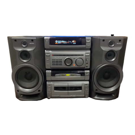
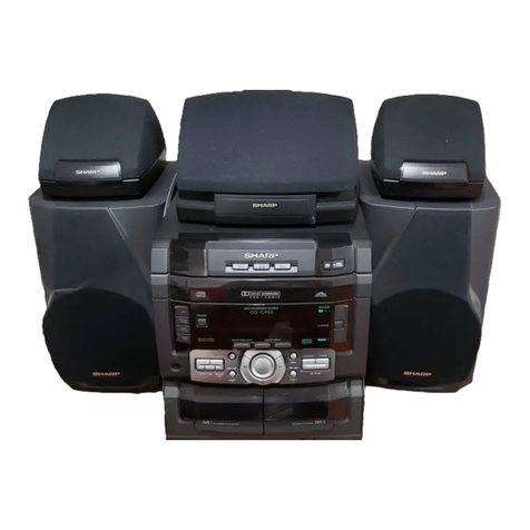
Sony HCR-S7AV User manual

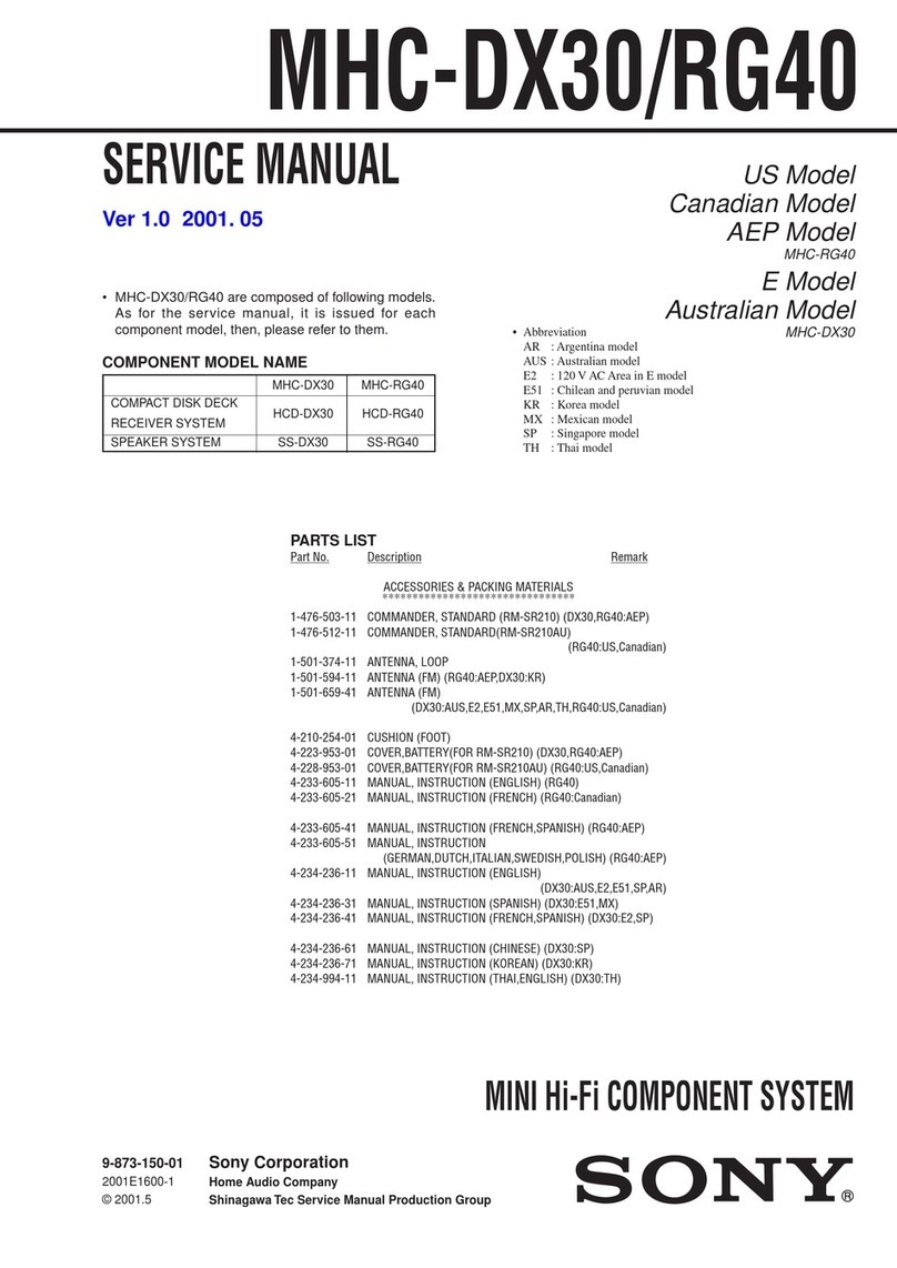
SERVICE MANUAL
9-873-830-11 Sony Corporation
2001D0500-1 Audio Entertainment Group
C2001.4 General Engineering Dept.
Ver 1.0 2001.04
MINI HiFi COMPONENT SYSTEM
AEP Model
UK Model
E Model
Australian Model
• MHC-S7AV is composed of following models.
As for the service manual, it is issued for each component model, then, please refer to it.
ACCESSORIES & PACKING MATERIALS
********************************
1-476-530-11 COMMANDER, STANDARD (RM-SR370AV)
1-501-374-11 ANTENNA, LOOP
1-501-659-71 ANTENNA (FM) (AUS, MX)
1-501-721-11 ANTENNA (LOOP)
1-501-804-11 ANTENNA (FM) (AEP, UK, KR)
1-574-264-11 CORD, LIGHT PLUG (OPTICAL)
1-769-306-11 CORD, SPEAKER (1.5m) (for SS-S9)
1-769-433-11 CORD, SPEAKER (10m) (for SS-RS270)
1-769-433-21 CORD, SPEAKER (2.5m) (for SS-CT270)
4-210-254-01 CUSHION (FOOT) (for SS-CT270/RS270)
4-233-737-11 MANUAL, INSTRUCTION (ENGLISH) (AEP, UK, AUS)
4-233-737-21 MANUAL, INSTRUCTION (FRENCH) (AEP)
4-233-737-31 MANUAL, INSTRUCTION (SPANISH) (AEP, MX)
4-233-737-41 MANUAL, INSTRUCTION (GERMAN, DUTCH, ITALIAN)
(AEP)
4-233-737-51 MANUAL, INSTRUCTION (SWEDISH) (AEP)
4-233-737-81 MANUAL, INSTRUCTION (KOREAN) (KR)
4-233-745-11 MANUAL, INSTRUCTION (DANISH, FINNISH) (AEP)
4-233-745-21 MANUAL, INSTRUCTION (PORTUGUESE) (AEP)
4-233-745-31 MANUAL, INSTRUCTION (RUSSIAN) (AEP)
4-233-745-41 MANUAL, INSTRUCTION (GREEK) (AEP)
4-233-745-51 MANUAL, INSTRUCTION (HUNGARIAN, CZECH) (AEP)
4-233-745-61 MANUAL, INSTRUCTION (TURKISH) (AEP)
4-233-745-71 MANUAL, INSTRUCTION (SLOVAKIAN) (AEP)
4-981-643-21 COVER, BATTERY (for RM-SR370AV)
PARTS LIST
Part No. Description Remark
MHC-S7AV
HCR-S7AV
•Abbreviation
AUS : Australian model
KR : Korea model
MX : Mexican model
SPECIFICATIONS
Power requirements
European model: 230 V AC, 50/60 Hz
Australian model: 230 – 240 V AC, 50/60 Hz
Mexican model: 120 V AC, 60 Hz
Korean model: 220 V AC, 60 Hz
Other models: 120 V, 220 V or 230 – 240 V AC, 50/60 Hz
Adjustable with voltage selector
Power consumption
European model: 300 watts
0.6 watts (during Power Saving Mode)
Other models: 300 watts
Dimensions (w/h/d)
TA-S7AV: Approx. 280 ×128 ×350 mm
ST-S5: Approx. 280 ×108 ×340 mm
CDP-S3: Approx. 280 ×108 ×330 mm
TC-S3: Approx. 280 ×128 ×330 mm
Mass
TA-S7AV: Approx. 7.7 kg
ST-S5: Approx. 2.1 kg
CDP-S3: Approx. 2.7 kg
TC-S3: Approx. 2.4 kg
Supplied accessories: AM loop antenna (1)
FM lead antenna (1)
Remote commander (1)
Batteries (2)
Speaker cords (5)
Optical cable (1)
Center and rear speaker pads (12)
Design and specifications are subject to change without notice.
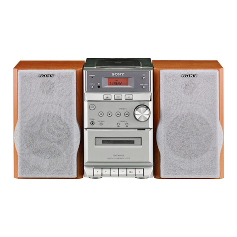
HCR-S7AV is composed of TA-S7AV, CDP-S3, TC-S3, ST-S5, SS-RS270 and SS-CT270.
COMPONENT MODEL NAME FOR MHC-S7AV.
MHC-S7AV
AMPLIFIER TA-S7AV
CD PLAYER CDP-S3
TAPE PLAYER TC-S3
FM STEREO, FM/AM SUPERHETERDYNE TUNER ST-S5
FRONT SPEAKER SS-S9
REAR SPEAKER SS-RS270
CENTER SPEAKER SS-CT270
SERVICE MANUAL
COMPACT DISC PLAYER
AEP Model
UK Model
E Model
Australian Model
SPECIFICATIONS
CDP-S3
Ver 1.0 2001.04
CDP-S3 is the CD player section
in MHC-S7AV or MHC-S3.
Model Name Using Similar Mechanism NEW
CD Mechanism Type CDM63B-30BD60
Base Unit Name BU-30BD60
Optical Pick-up Name OP Assy (A-MAX.3)
System Compact disc and digital
audio system
Laser Semiconductor laser
(λ=780 nm)
Emission duration:
continuous
Frequency response 2 Hz – 20 kHz (±0.5 dB)
Signal-to-noise ratio More than 90 dB
Dynamic range More than 90 dB
OPTICAL OUT
(Square optical connector jack, rear panel)
Dimensions (w/h/d)
Approx. 280 x 108 x 330 mm
Mass Approx. 2.7 kg
Design and specifications are subject to change
without notice.
9-873-831-11 Sony Corporation
2001D0500-1 Home Audio Company
C2001.4 ShinagawaTec Service Manual Production Group

2
CDP-S3
SAFETY-RELATED COMPONENT WARNING!!
COMPONENTS IDENTIFIED BY MARK 0OR DOTTED
LINE WITH MARK 0ON THE SCHEMATIC DIAGRAMS
AND IN THE PARTS LIST ARE CRITICAL TO SAFE
OPERATION. REPLACE THESE COMPONENTS WITH
SONY PARTS WHOSE PART NUMBERS APPEAR AS
SHOWN IN THIS MANUAL OR IN SUPPLEMENTS PUB-
LISHED BY SONY.
The laser diode in the optical pick-up block may suffer electro-
static break-down because of the potential difference generated
by the charged electrostatic load, etc. on clothing and the human
body.
During repair, pay attention to electrostatic break-down and also
use the procedure in the printed matter which is included in the
repair parts.
The flexible board is easily damaged and should be handled with
care.
NOTES ON LASER DIODE EMISSION CHECK
The laser beam on this model is concentrated so as to be focused
on the disc reflective surface by the objective lens in the optical
pick-up block. Therefore, when checking the laser diode emis-
sion, observe from more than 30 cm away from the objective lens.
LASER DIODE AND FOCUS SEARCH OPERATION
CHECK
Carry out the “S curve check”in “CD section adjustment”and
check that the S curve waveforms is output three times.
Notes on chip component replacement
•Never reuse a disconnected chip component.
•Notice that the minus side of a tantalum capacitor may be dam-
aged by heat.
Flexible Circuit Board Repairing
•Keep the temperature of the soldering iron around 270 ˚C dur-
ing repairing.
•Do not touch the soldering iron on the same conductor of the
circuit board. (within 3 times)
•Be careful not to apply force on the conductor when soldering
or unsoldering.
NOTES ON HANDLING THE OPTICAL PICK-UP
BLOCK OR BASE UNIT CAUTION
Use of controls or adjustments or performance of procedures
other than those specified herein may result in hazardous ra-
diation exposure.
This appliance is classified as a CLASS 1 LASER product.
The CLASS 1 LASER PRODUCT MARKING is located on
the rear exterior.
Laser component in this product is capable of emitting radiation
exceeding the limit for Class 1.
The following caution label is located inside the unit.

3
CDP-S3
TABLE OF CONTENTS
1. SERVICING NOTES ............................................... 4
2. GENERAL ................................................................... 5
3. DISASSEMBLY
3-1. Disassembly Flow ........................................................... 6
3-2. Cover ............................................................................... 7
3-3. CD Mechanism Deck (CDM63B-30BD60) ................... 7
3-4. MAIN Board ................................................................... 8
3-5. Front Panel Section ......................................................... 8
3-6. PANEL (L) Board, PANEL (R) Board ........................... 9
3-7. Lid (CD) .......................................................................... 9
4. TEST MODE.............................................................. 10
5. ELECTRICAL ADJUSTMENTS......................... 11
6. DIAGRAMS
6-1. Note for Printed Wiring Boards
and Schematic Diagrams ................................................ 12
6-2. Printed Wiring Board –BD Section –........................... 14
6-3. Schematic Diagram –BD Section –............................... 15
6-4. Printed Wiring Boards –CD CHANGER Section –..... 16
6-5. Schematic Diagram –CD CHANGER Section –......... 17
6-6. Printed Wiring Board –MAIN Section –...................... 18
6-7. Schematic Diagram –MAIN Section –......................... 19
6-8. Printed Wiring Boards –PANEL Section –.................. 20
6-9. Schematic Diagram –PANEL Section –....................... 21
6-10. IC Pin Function Description ........................................... 24
7. EXPLODED VIEWS
7-1. General Section ............................................................... 26
7-2. CD Mechanism Deck Section-1
(CDM63B-30BD60) ....................................................... 27
7-3. CD Mechanism Deck Section-2
(CDM63B-30BD60) ....................................................... 28
7-4. Base Unit Section (BU-30BD60) ................................... 29
8. ELECTRICAL PARTS LIST ............................... 30

4
CDP-S3 SECTION 1
SERVICING NOTES
This set is a component of the MHC-S7AV or MHC-S3.
The MHC-S7AV or MHC-S3 system configuration is as shown
below, and therefore it does not operate normally unless all four
components are connected.
In performing the repair, connect all components with the system
cables.
Note:The precaution to the users is described on the label stuck on
the back panel (CD player) and in the troubleshooting section in
the Operation Manual.
System Configuration:
POWER SUPPLY
AC IN
TA
SYSTEM & CD
µ
con
ST
CDP
TC
µ
con
TC
DISPLAY
CD-TEXTTEST DISC
This unit is able to display the test data (character information)
written in the CD on its fluorescent indicator tube.
The CD-TEXT TEST DISC (TGCS-313:4-989-366-01) is used
for checking the display.
To check, perform the following procedure.
Checking Method:
1. Press the I/1button to turn the power on, set the disc to the
disc table with the “test disc”label facing up, and chuck the
disc.
2. Press the [CD] button to set CD function, and press the
n N button to playback the disc.
3. The following will be displayed on the liquid crystal display.
Display : 1KHZ/0DB/L R
4. Pressing the [-- ] or [ +] button, select the track. The text
data of each track will be displayed.
Fordetails of the displayedcontentsfor each track, referto “Table
1 : CD-TEXT TEST DISC TEXT Data Contents”.
Restrictions in CD-TEXT Display
In this unit, some special characters will not be displayed prop-
erly. These will be displayed as a space or a character resembling
it.
Table 1 : CD-TEXTTEST DISC TEXT Data Contents
(TRACKS No. 1 to 20:Normal Characters)
1 1kHz/0dB/L&R
2 20Hz/0dB/L&R
3 40Hz/0dB/L&R
4 100Hz/0dB/L&R
5 200Hz/0dB/L&R
6 500Hz/0dB/L&R
7 1kHz/0dB/L&R
8 5kHz/0dB/L&R
9 7kHz/0dB/L&R
10 10kHz/0dB/L&R
11 16kHz/0dB/L&R
12 18kHz/0dB/L&R
13 20kHz/0dB/L&R
14 1kHz/0dB/L&R
15 1kHz/–1dB/L&R
16 1kHz/–3dB/L&R
17 1kHz/–6dB/L&R
18 1kHz/–10dB/L&R
19 1kHz/–20dB/L&R
20 1kHz/–60dB/L&R
TRACK
No. Displayed Contents
Note: Track No. 21 to 99 are not displayed.
.>

5
CDP-S3
SECTION 2
GENERAL This section is extracted from
instruction manual.
Parts Identification
The items are arranged in alphabetical order.
Refer to the pages indicated in parentheses ( ) for details.
Main unit
mM
.
HS x
>
1 2 3
wj wkwl e; ea
es
ed
efegehej
ek
DISC 1–3 ek (14, 15, 21)
DISC 1–3 indicators ej
DISC 1–3 Z(eject) wl (14)
PLAY MODE wj (14, 15, 21)
REPEAT wk (14)
N(play) eh (14, 15)
X(pause) eg (14)
x(stop) ef (14, 20)
.(go back) ed (14, 15, 21)
>(go forward) es (14, 15, 21)
m(rewind) e; (14)
M(fast forward) ea (14)
x
hH
H
hH
O
o
Pp
Mm X
>
.
123
wg
qh
qa
wk
wj
wh
wa
4
5
6
7
qs
qf
qd
qg
8
9
q;
qk
ql
w;
qj
wd
ws
wf
es
ea
e;
wl
CD Hes (14, 15)
CHECK 5(15)
CLEAR 6(15)
CLOCK/TIMER SELECT qj
(30)
CLOCK/TIMER SET qk (13, 21,
29)
DBFB qg (23)
DISPLAY ws (13, 16, 18, 29, 35)
D.SKIP 4(14)
ENTER wg (10, 12, 13, 15, 17,
18, 21, 22, 26–30)
EQ qd (27)
EQ ON/OFF qf (10, 28)
FUNCTION wf (10, 14, 15, 20,
21, 31)
GROOVE wa (23)
SET UP qs (10, 12, 26, 28, 29)
SLEEP 7(29)
SUR wd (25)
TAPE A hH ea (19, 35)
TAPE B hH e; (19, 20, 35)
TUNER/BAND wl (17)
TUNING + 9(17)
TUNING –wh (17)
TV CH +/–ql
TV VOL +/–w;
TV @/1 2
TV/VIDEO 1
VOL +/–qh
BUTTON DESCRIPTIONS
@/1 (power) 3
X(pause) q;
x(stop) 8
.(go back) wk
>(go forward) wj
m(rewind) wh
M(fast forward) 9
O/o/P/pqa
Remote Control

CDP-S3
6
•This set can be disassembled in the order shown below.
3-1. DISASSEMBLY FLOW
SECTION 3
DISASSEMBLY
3-2. COVER
(Page 7)
3-3. CD MECHANISM DECK
(CDM63B-30BD60)
(Page 7)
3-6. PANEL (L) BOARD,
PANEL (R) BOARD
(Page 9)
3-7. LID (CD)
(Page 9)
3-5. FRONT PANEL SECTION
(Page 8)
3-4. MAIN BOARD
(Page 8)
SET

CDP-S3
7
3-3. CD MECHANISM DECK (CDM63B-30BD60)
Note: Follow the disassembly procedure in the numerical order given.
3-2. COVER
1
two screws
(case 3 TP2)
3
cover
2
screw
(BVTT3
×
6)
1
two screws
(case 3 TP2
)
3
four screws
(BVTP3
×
8)
1
wire (flat type) (21 core)
(CN301)
2
connecto
r
(CN701)
4
CD mechanism deck
(CDM63B-30BD60)

CDP-S3
8
3-4. MAIN BOARD
3-5. FRONT PANEL SECTION
2
connector
(CN401)
1
wire (flat type) (21 core)
(CN301)
2
two connectors
(CN101, 102)
5
MAIN board
3
screw
(BVTP3
×
8)
4
lug
3
screw
(BVTP3
×
8)
2
connector
(CN701)
3
two screws
(BVTP3
×
8
)
2
three screws
(BVTP3
×
8)
3
two claws
1
connector
(CN401)
4
front panel section
3
claw

CDP-S3
9
3-6. PANEL (L) BOARD, PANEL (R) BOARD
3-7. LID (CD)
5
two claws
4
four screws
(BVTP2.6
×
8)
6
PANEL (R) board
1
five screws
(BVTP2.6
×
8)
3
PANEL (L) boar
d
2
two claws
3
lid (CD)
4
spring (CD)
1
screw
(BVTP2.6
×
8
)
2
bracket (LID) assy

10
CDP-S3 SECTION 4
TEST MODE
Note: Use flowing buttons in the test mode.
no mark: Button of CD unit (CDP-S3)
*1 : Button of amplifier unit (TA-S7AV or TA-S3)
*2 : Button of tuner unit (ST-S5 or ST-S3)
[CD Delivery Mode]
•This mode moves the optical pick-up to the position durable to
vibration. Use this mode when returning the set to the customer
after repair.
Procedure:
1. Press the I/1*1button to turn the power on.
2. Turn the [FILE SELECT] *1knob to set the CD function.
3. While pressing the [EQ ON/OFF] *1button, press the I/1*1
button.
4. The message “LOCK”is displayed on the fluorescent indica-
tor tube of tuner unit and turn the power off automatically, and
the CD delivery mode is set.
[GCTest Mode]
Enter the GCTest Mode
Procedure 1:
1. Press the I/1*1button to turn the power on.
2. While pressing the both [PLAY MODE] and [ ] buttons, press
the [ ] (DISC 1) button.
3. LEDs and fluorescent indicator tube are all turned on of all
units.
Procedure 2:
1. Press the I/1*1button to turn the power on.
2. While pressing the both [STEREO/MONO] *2and
[CINEMA STUDIO C] *1 buttons, press the [CLOCK/TIMER]
*2button.
3. LEDs and fluorescent indicator tube are all turned on of all
units.
Version Display Mode
Procedure:
1. Enter the GC test mode.
2. Each time the [DISC 1] or [TUNER MEMORY] *2button is
pressed, microcomputer or mechanism deck version is dis-
played of each unit.
3. Press the [DISC 3] or [TUNING +] *2button to detail is dis-
played the version.
Key Check Mode
Procedure:
1. Enter the GC test mode.
2. Press the [DISC 2] or [TUNING --] *2button to set the key
check mode, and displays “K 0 J 0 V 0”on the fluorescent
indicator tube of tuner unit.
3. All buttons are pressed of CD unit, all LEDs are blinking of
CD unit. (not change the display of fluorescent indicator tube)
Releasing the GCTest Mode
To release from this mode, press three buttons in the same manner
as entering this mode or disconnect the power cord.
x
Z
[CD Service Mode]
•This mode can run the CD sled motor optionally. Use this mode,
for instance, when cleaning the optical pick-up.
Procedure:
1. Press the I/1*1button to turn the power on.
2. Turn the [FILE SELECT] *1knob to set the CD function.
3. While pressing the both [PLAY MODE] and [ ] buttons, press
the [ ] button.
4. Set to the CD service mode.
5. With the CD in stop status, press the [ ] button to move the
optical pick-up to outside track, or press the [ ] button to
inside track.
6. To release from this mode, perform as follows.
1) Move the optical pick-up to the most inside track.
2) Disconnect the power cord.
Notes: •Always move the optical pick-up to most inside track when
releasing from this mode. Otherwise, a disc will not be un-
loaded.
•Do not run the sled motor excessively, otherwise the gear can
be chipped.
[CD Cancellation Mode of Repeat Limitation]
•This mode can cancel the CD repeat limitation (5 times).
Procedure:
1. Press the I/1*1button to turn the power on.
2. Turn the [FILE SELECT] *1knob to set the CD function.
3. While pressing the both [PLAY MODE] and [ ] buttons, press
the [REPEAT] button.
4. CD repeat limitation is canceled.
5. To release this mode, disconnect the power cord.
x
.
M
m
x

11
CDP-S3
SECTION 5
ELECTRICAL ADJUSTMENTS
Note :
1. CD Block is basically designed to operate without adjustment.
Therefore, check each item in order given.
2. Use LUV-P01 (4-999-032-01) unless otherwise indicated.
3. Use an oscilloscope with more than 10MΩimpedance.
4. Clean the object lens by an applicator with neutral detergent
when the signal level is low than specified value with the
following checks.
S-Curve Check
Procedure :
1. Connect an oscilloscope to TP (FEO).
2. Connect between TP (FEI) and TP (DVC) ( 1.65 V) by lead
wire.
3. Turn Power switch on.
4. Load a disc (LUV-P01) and actuate the focus search. (In
consequence of open and close the disc tray, actuate the focus
search)
5. Confirm that the oscilloscope waveform (S-curve) is
symmetrical betweenA and B.And confirm peak to peak level
within 2 ±0.5 Vp-p.
6. After check, remove the lead wire connected in step 2.
Note : •Try to measure several times to make sure than the ratio
of A : B or B :A is more than 10 : 7.
•Take sweep time as long as possible and light up the
brightness to obtain best waveform.
RF Level Check
Procedure :
1. Connect an oscilloscope CH1 to TP (RFDC) and CH2 to TP
(RFAC).
2. Turn Power switch on.
3. Load a disc (LUV-P01) and playback.
4. Confirm that oscilloscope waveform is clear and check if RF
signal level is correct or not.
Note : Clear RF signal waveform means that the shape “◊”can be clearly
distinguished at the center of the waveform.
BD board Oscilloscope
TP(FEO)
TP(DVC)
symmetry
S-curve waveform
within 2
±
0.5Vp-
p
A
B
TP(RFDC)
TP(RFAC)
BD board oscilloscope
TP(DVC)
E-F Balance (1Track jump) Check
Procedure :
1. Connect an oscilloscope to TP (TEO) and TP (DVC).
2. Turn Power switch on.
3. Load a disc (LUV-P01) and playback the number nine track.
4. Press the Nbutton. (Becomes the 1 track jump mode.)
5. Confirm that the level B andA (DC voltage) on the oscilloscope
waveform.
6. Adjust RV101 on the BD board so that the center of waveform
becomes the same voltage of DVC. (i.e. A=0V)
Adjustment Location:
[BD BOARD] (Conductor Side)
RF signal waveform VOLT/DIV : 200mV
TIME/DIV : 500ns
level : 0.65
±
0.15Vp-p (RFDC)
1.1
±
0.4Vp-p (RFAC)
TP(TEO)
TP(DVC)
BD board oscilloscop
e
level=1.0
±
0.5Vp-p symmetry
A (DC voltage
)
center of
waveform
B
DVC
1 track jump waveform
TP (TEO)
TP
(RFAC)
TP
(FEI) TP
(RFDC)
TP (FEO) IC101
IC103
RV101
TP (DVC)
1
15
30
1
2021
40
60
80
41
61
16

12
CDP-S3 SECTION 6
DIAGRAMS
C
BThese are omitted.
E
Q
B
These are omitted.
CE
Q
Note on PrintedWiring Boards:
•X: parts extracted from the component side.
•Y: parts extracted from the conductor side.
•f: internal component.
•: Pattern from the side which enables seeing.
• Indication of transistor.
Note on Schematic Diagram:
• All capacitors are in µF unless otherwise noted. pF: µµF
50 WV or less are not indicated except for electrolytics
and tantalums.
• All resistors are in Ωand 1/4W or less unless otherwise
specified.
•f: internal component.
•C: panel designation.
•A: B+ Line.
• Voltagesaretaken withaVOM(Inputimpedance10MΩ).
Voltage variations may be noted due to normal produc-
tion tolerances.
• Waveforms are taken with a oscilloscope.
Voltage variations may be noted due to normal produc-
tion tolerances.
• Circled numbers refer to waveforms.
• Signal path.
J: CD PLAY
Note: The components identified by mark 0or dotted line
with mark 0are critical for safety.
Replace only with part number specified.
6-1. NOTE FOR PRINTED WIRING BOARDS AND SCHEMATIC DIAGRAMS
(In addition to this, the necessary note is printed in each block)

13
CDP-S3
• Circuit Boards Location
DISC SENSOR board
BD board
IN OUT SW board
MOTOR board
DRIVER boar
d
TRAY SENSOR board
MAIN board
PANEL (L) board
PANEL (R) board

14
CDP-S3
6-2. PRINTED WIRING BOARD – BD Section – • See page 13 for Circuit Boards Location.
There are a few cases that the part printed on
this diagram isn’t mounted in this model.
• Semiconductor
Location
Ref. No. Location
MAIN
BOARD
CN301
M102
(SLED)
TP
(RFDC)
TP
(RFAC)
TP
(FEI)
TP
(DVC)
TP (TEO)
TP
(FEO)
M101
(SPINDLE)
A
D101 B-3
IC101 C-3
IC102 B-2
IC103 D-2
Q101 C-1
Q102 A-3
(Page 18)

CDP-S3
1515
TP
(RFDC)
TP (DVC)
TP
(TEO)
TP
(FEO)
TP (FEI)
TP
(RFAC)
IC B/D
IC B/D
IC B/D
MAIN
BOARD
CN301
A
6-3. SCHEMATIC DIAGRAM –BD Section –•See page 22 forWaveforms. •See page 22 for IC Block Diagrams.
•Voltages and waveforms are dc with respect to ground
under no-signal conditions.
no mark : CD PLAY
Note: The components identified by mark 0or dotted line
with mark 0are critical for safety.
Replace only with part number specified.
(Page 19)

CDP-S3
1717
6-5. SCHEMATIC DIAGRAM –CD CHANGER Section –•See page 22 for IC Block Diagram.
•Voltages and waveforms are dc with respect to ground
under no-signal conditions.
no mark : CD STOP
B
MAIN
BOARD
NO202
IC731
SUB TRAY1
HEIGHT SENSOR
IC732
SUB TRAY2
HEIGHT SENSOR
IC733
SUB TRAY3
HEIGHT SENSOR
IC751
DISC IN
DETECT
(Page 19)

CDP-S3
1818
6-6. PRINTED WIRING BOARD –MAIN Section –•See page 13 for Circuit Boards Location.
Ref. No. Location
Ref. No. Location
•Semiconductor Location
D501
C401
CN301
C101
JW115
C501
CN102
CN101
CN401
D502
D503
D504
R403
FB305
FB410
R409
C462
C463
C103
IC502
IC503
C513
C532
C523
D123
C500
R480
Q501
Q502
R448
R123
JW157
JW167
JW168
JW143
JW153
JW130
R460
C317
C318 C316
JW108
JW100
D514
JW103
X401
C531
JW137
R425
C319
R483
D511
C524
JW114
JW122
R419
JW126
R436
R401
R402
JW119
JW131
R413
C124
D513
JW113
C303
C522
R486
R485
JW110
C302
JW109
JW132
R487
JW104
C102
IC102
CN103
C122
CD304
JW133
R495
R484
JW125
C260
C261
C255
JW121
JW127
JW128
JW163
JW129
FB416
JW112
JW118
JW117
JW106
C251
JW138
R497
C499
JW171
JW124
JW144
CD302
JW145
JW149
R428
JW141
C498
R426
JW146
JW164
JW156
JW155
R433
JW160
C411
R432
JW123
R411
R427
C416
R417
JW120
JW139
CD303
JW142
D515
R424
R429
R430
R442
C425 C427
R493
JW159
R456
R441
R443
R490
R438
R496
R445
R449
R450
R446
R447
R452
R500
R453
JW147
R473
R469
R465
R477
R481 JW148
JW111
R444
JW169
R494
R482
R491
R489
R132
R133
R134
L125
R492
JW162
JW165
JW135
JW170
R412
JW136
CD301
CD311
CD312
JW134
JW172
R459
R457
JW161
NO202
JW102
D105
VCD101
JW99
JW116
JW98
C301
JW175
JW177
JW150
C521
JW176
C125
JW140
CLP101
FB313
L310
FB314
FB315
C320 C311
FB310
FB311
FB312
R451
JW178
C321
JW158
C314
R437 C313
CD313
C315
R440
R435
C304
JW154
C310
JW151
JW107
D512
C306
IC402
IC401
112
C118
C116
C107
CLP102
BD BOARD
CN101
A
PANEL (L) BOARD
NO703
C
DRIVER BOARD
CN701
B
1
9
1
1
14
8
E
E
3
1
3
18
1
9
1
1
15
2
14
1
3
1-680-994-
11
(21)
(CHASSIS)
OPTICAL OUT
TO ST-S3/S5
SYSTEM CONTROL 5
TO TC-S3
SYSTEM CONTROL 3
TO ST-S3/S5
MAIN BOARD
A
B
C
D
1 2 3 4 5 6 7 8 9 10
D103 D-9
D104 D-9
D105 D-7
D123 B-8
D501 C-9
D502 C-9
D503 C-9
D504 C-9
D511 C-8
D512 D-7
D513 B-8
D514 B-8
IC102 D-10
IC401 C-4
IC402 B-5
IC502 C-8
IC503 B-8
Q501 C-8
Q502 C-8
(Page 14) (Page 16)
(Page 20)
This manual suits for next models
1
Table of contents
Other Sony Stereo System manuals

Sony
Sony MHC-GTR8 User manual

Sony
Sony HCD-EC55 - Receiver System User manual

Sony
Sony HCD-RXD6AV User manual

Sony
Sony HCD-RG88 User manual

Sony
Sony HCD-VX777 User manual

Sony
Sony HCD-H1700 User manual

Sony
Sony ZS-RS60BT User manual

Sony
Sony HCD-GRX3 User manual

Sony
Sony MHC-V42D Reference guide

Sony
Sony LBT-XG60 User manual

Sony
Sony HCD-XGR6 User manual

Sony
Sony HCD-V8800 User manual

Sony
Sony HCD-EX1 User manual

Sony
Sony MHC-GN1300D User manual

Sony
Sony BDV-N995W User manual

Sony
Sony HCD-RXD7AV User manual

Sony
Sony HCD-VZ0 User manual

Sony
Sony HCD-CP300 User manual

Sony
Sony CMTBX1 - CMT BX1 Micro System User manual

Sony
Sony HCD-MD555 User manual