Sony HCD-EX1 User manual

1
HCD-EX1
US Model
Canadian Model
AEP Model
UK Model
E Model
Australian Model
Tourist Model
COMPACT COMPONENT SYSTEM
MICROFILM
SERVICE MANUAL
SPECIFICATIONS
Model Name Using Similar Mechanism NEW
Mechanism Type CDM-60
Base Unit Type KSM-770ACA/S-NP
Optical Pick-up Type KSS-770A/S-N1
HCD-EX1 is the amplifier, CD and
tuner section in CMT-EX1.

2
SAFETY CHECK-OUT
After correcting the original service problem, perform the follow-
ing safety checks before releasing the set to the customer:
Checktheantennaterminals,metaltrim,“metallized”knobs,screws,
and all other exposed metal parts forAC leakage. Check leakage as
described below.
LEAKAGE
The AC leakage from any exposed metal part to earth Ground and
from all exposed metal parts to any exposed metal part having a
return to chassis, must not exceed 0.5 mA(500 microampers). Leak-
age current can be measured by any one of three methods.
1. A commercial leakage tester, such as the Simpson 229 or RCA
WT-540A. Follow the manufacturers’ instructions to use these
instruments.
2. A battery-operated AC milliammeter. The Data Precision 245
digital multimeter is suitable for this job.
3. Measuring the voltage drop across a resistor by means of a VOM
or battery-operatedAC voltmeter. The “limit” indication is 0.75
V, so analog meters must have an accurate low-voltage scale.
The Simpson 250 and Sanwa SH-63Trd are examples of a pas-
sive VOM that is suitable. Nearly all battery operated digital
multimeters that have a 2VAC range are suitable. (See Fig. A)
Fig. A. Using an AC voltmeter to check AC leakage.
0.15
µ
F
To Exposed Metal
Parts on Set
1.5k
Ω
AC
voltmeter
(0.75V)
Earth Ground
SAFETY-RELATED COMPONENTWARNING !!
COMPONENTS IDENTIFIED BY MARK !OR DOTTED LINE
WITH MARK !ON THE SCHEMATIC DIAGRAMS AND IN
THE PARTS LIST ARE CRITICAL TO SAFE OPERATION.
REPLACE THESE COMPONENTS WITH SONY PARTS
WHOSE PART NUMBERS APPEAR AS SHOWN IN THIS
MANUAL OR IN SUPPLEMENTS PUBLISHED BY SONY.
CAUTION
Use of controls or adjustments or performance of procedures
other than those specified herein may result in hazardous ra-
diation exposure.
Notes on chip component replacement
• Never reuse a disconnected chip component.
• Notice that the minus side of a tantalum capacitor may be
damaged by heat.
Flexible Circuit Board Repairing
• Keep the temperature of soldering iron around 270˚C
during repairing.
• Do not touch the soldering iron on the same conductor of the
circuit board (within 3 times).
• Be careful not to apply force on the conductor when soldering
or unsoldering.
Laser component in this product is capable of emitting radiation
exceeding the limit for Class 1.
This appliance is classified as
a CLASS 1 LASER product.
The CLASS 1 LASER PROD-
UCT MARKING is located on
the rear exterior.
This caution
label is located
inside the unit.
ATTENTION AU COMPOSANT AYANT RAPPORT
À LA SÉCURITÉ!!
LESCOMPOSANTS IDENTIFIÉS PAR UNE MARQUE!SUR
LES DIAGRAMMES SCHÉMATIQUES ET LA LISTE DES
PIÈCES SONT CRITIQUES POUR LA SÉCURITÉ DE
FONCTIONNEMENT.NE REMPLACER CES COMPOSANTS
QUE PAR DES PIÈCES SONY DONT LES NUMÉROS
SONT DONNÉS DANS CE MANUEL OU DANS LES
SUPPLÉMENTS PUBLIÉS PAR SONY.

3
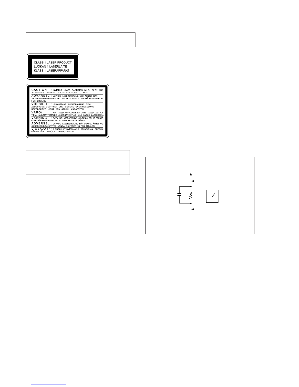
NOTES ON HANDLINGTHE OPTICAL PICK-UP BLOCK
OR BASE UNIT
The laser diode in the optical pick-up block may suffer electrostatic
break-down because of the potential difference generated by the
charged electrostatic load, etc. on clothing and the human body.
During repair, pay attention to electrostatic break-down and also
use the procedure in the printed matter which is included in the
repair parts.
The flexible board is easily damaged and should be handled with
care.
NOTES ON LASER DIODE EMISSION CHECK
The laser beam on this model is concentrated so as to be focused on
the disc reflective surface by the objective lens in the optical pick-
up block. Therefore, when checking the laser diode emission, ob-
serve from more than 30 cm away from the objective lens.
LASER DIODE AND FOCUS SEARCH OPERATION
CHECK
Carryout the “S curve check” in “CD sectionadjustment” and check
that the S curve waveform is output four times.
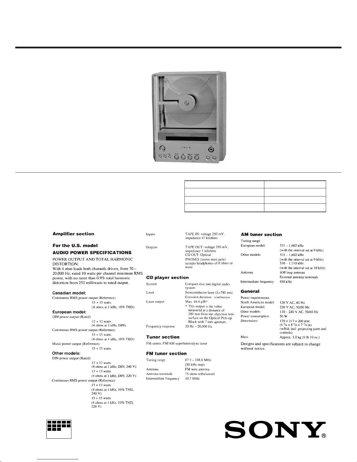
TABLE OF CONTENTS
1. SERVICING NOTE .......................................................... 4
2. GENERAL .......................................................................... 7
3. DISASSEMBLY
3-1. Back Cover and Case ............................................................ 9
3-2. Panel Board and Stabilizer .................................................... 9
3-3. AMP Block ......................................................................... 10
3-4. CD Block ............................................................................ 10
3-5. Motor ASSY and CAM ....................................................... 11
3-6. Base Unit............................................................................. 11
3-7. Main Board and Power Board ............................................ 12
4. ELECTRICAL ADJUSTMENT ..............................13
5. DIAGRAMS
5-1. Circuit Boards Location ...................................................... 14
5-2. Printed Wiring Board – Main Section –.............................. 16
5-3. Schematic Diagram – Main (1/3) Section –........................ 18
5-4. Schematic Diagram – Main (2/3) Section –........................ 19
5-5. Schematic Diagram – Main (3/3) Section – ........................ 20
5-6. Printed Wiring Board – LED/Loading/SW Section – ......... 21
5-7. Schematic Diagram
– LED/Loading/SW Section Section – ............................... 21
5-8. Printed Wiring Board – AMP Section – .............................. 22
5-9. Schematic Diagram – AMP Section –................................. 23
5-10. Printed Wiring Board – Panel Section –........................... 24
5-11. Schematic Diagram – Panel Section – ............................. 25
5-12. Printed Wiring Board – Power Section – ......................... 26
5-13. Printed Wiring Board – Power Section – ......................... 27
5-14. Printed Wiring Board – REG Section –............................28
5-15. Schematic Diagram – REG Section – .............................. 29
5-16. IC Block Diagrams ........................................................... 30
5-17. IC Pin Functions ............................................................... 32
6. EXPLODEDVIEWS
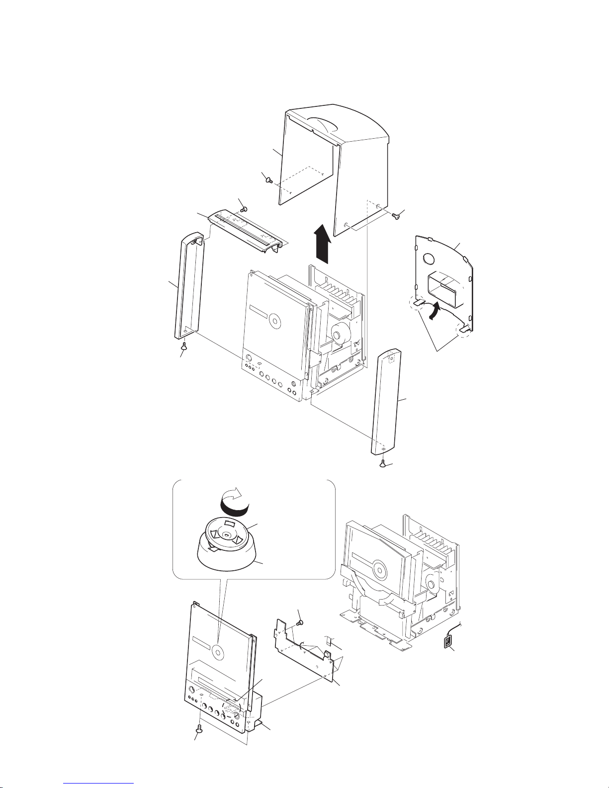
6-1. Front and Case Section ....................................................... 36
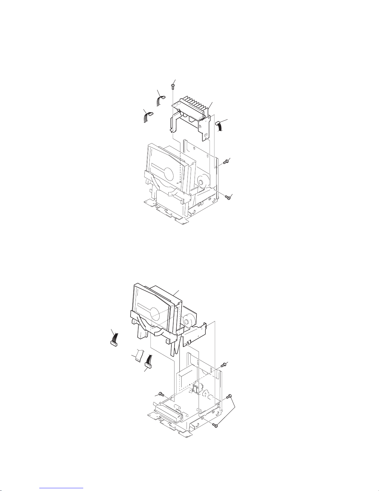
6-2. Chassis Section ................................................................... 37
6-3. Mechanism Section ............................................................. 38
6-4. Base Unit Section................................................................ 39
7. ELECTRICAL PARTS LIST .................................40

4
SECTION 1
SERVICING NOTE
ADJUSTMENT OF CAM PHASE
Absorber Absorber
SW lever SW lever
Boss
Cam
Slider (3)
Screw
(BVTP2.6x8)
Screw
(PTTWH2.6x8)
Screw
(BVTP2.6x8)
Groove of slider (3)
Hole of slider (3)
Guide (L)
Boss (Four point)
Guide (R)
Slider (2)
Lever (1)
Lever (1)
Mecha cover
Cam
Boss Boss
Boss
Cam
Boss
Insert the cam so that the boss touches the SW lever
at the left shown in the figure. Rotate the cam in the arrow direction, and adjust the
phase until the boss touches the SW lever shown in
the figure.
With the phase adjusted, attach the parts using the following procedure.
STEP1
Insert the boss of the slider (3) in the groove of
the cam.
STEP2
Set the mecha cover to the groove
on the slider (3) and attach.
STEP3
Insert the boss of the lever (1) in the hole of the
slider (3) and attach.
STEP4
While bending the slider (2) slightly in the arrow
direction, insert it in the groove of the guides (L)
and (R) and attach.

5
Shipment Mode
• Mode for setting the state of the unit to the state at shipment. When returning the unit to the customer after completing servicing, set to the
shipment mode.
Procedure :
Connect the power plug to the outlet while pressing the 1/ubutton.
Change-over of AM tuner Step between 9kHz and 10kHz.
• A step of AM channels can be changed over between 9kHz and 10kHz.
Procedure:
1. Press 1/ubutton to turn on the set ON.
2. Select the function “TUNER”, and press the TUNER/BAND button to select the BAND “AM”.
3. Press the 1/ubutton to turn on the set OFF.
4. Press 1/ubutton while pressing the )+/TUNING + button, and the display of liquid crystal indicator tube changes to “AM 9k
STEP” or “AM 10k STEP”, and thus the channel step is changed over.
Switching theTAPE IN input level attenuate function ON/OFF
• The attenuate function of the line input level (TAPE IN) of this unit can be turned ON/OFF.
Procedure:
1. Press the 1/ubutton to turn ON the power.
2. Press the FUNCTION button and set the function to “TAPE”.
3. Press the 1/ubutton to turn OFF the power.
4. While pressing the pbutton, press the 1/ubutton to turn ON the power.
5. After “POWER ON” is displayed, “ATT ON” and “ATT OFF” are displayed, and the attenuate function can be switched ON/OFF.
LCD All Lit and Key Check Mode
Procedure:
1. While pressing the FUNCTION button and ^button, connect the power plug to the outlet.
2. When the test mode is set, the characters “STEP” are displayed on the LCD.
3. While pressing the DISPLAY button, press the ^button. The whole LCD lights up.
4. Each time the FUNCTION button is pressed, the display switches between all lit npartial lighting 1 npartial lighting 2 nall lit.
5. When the pbutton is pressed, “KEY 0” is displayed and the key check mode is set.
6. Each time the button is pressed, the counter counts up. Buttons once pressed will not be counted when pressed again.
When all buttons have been pressed, “KEY OK” is displayed.
7. To end, press the 1/ubutton to turn OFF the power, and disconnect the power plug from the outlet.
Note:
Pressing buttons other than those specified in steps 4 and 5 displays modes not used in servicing. In such cases, press the 1/ubutton to exit
the mode, and repeat from step 3 again.
All lit
Partial lighting 1
Partial lighting 2

6
Displaying the CDText
• This unit is equipped with a simple CD text display function.
The text is displayed only for the first 20 songs. As it will not be displayed from the 21st song, do not suspect a fault.
In some cases, special characters may not be displayed or may be substituted by other characters. This is not a fault.
Aging Mode
• The aging mode automatically repeats the operations of the CD.
When an error occurs:
Aging stops
When no error occurs:
Aging is performed repeatedly.
Procedure:
1. Set any CD. (One with a short playback time of the final track is recommended.)
2. While pressing the FUNCTION button and ^button, connect the power plug to the outlet.
3. When the test mode is set, the characters “STEP” is displayed on the LCD.
4. When the ^button is pressed while pressing the DISPLAY button, “AGING” will be displayed, and aging is performed in the
following sequence. While aging is performed, “REP” will be displayed blinking.
5. Pressing the DISPLAY button during aging displays the cycle number (@ CY where @ is the number of agings).
6. To end aging, press the 1/ubutton, turn OFF the power, and disconnect the power plug from the outlet.
Sequence during aging
Reads the TOC
Pauses
Accesses first track
Accesses last track
Plays last track
Eject disc (“OPEN” displayed)
Load disc (“CLOSE” displayed)
Displays number of cycles
Power OFF
Power ON

7
LOCATION OF PARTS AND CONTROLS
11/u (power) button
2DISC tray
3Display window
46button
5VOLUME + button
6VOLUME – button
7)+/TUNING + button
8=0/TUNING – button
9p(stop) button
10 ^button
11 TUNER/BAND button
12 FUNCTION button
13 DISPLAY button
SECTION 2
GENERAL
2
14
3
7
913 8 56
10
1112
Remote
1
2
4
3
7
9
8
5
6
10
11
12
13
14
17
19
18
15
16
20
21
22
1OPEN/CLOSE button
2CD ·button
3TUNER/BAND button
4FUNCTION button
5CD PLAY MODE button
6TUNING MODE button
7MEMORY button
8ENTER button
9TIMER SET button
10 SLEEP button
11 TIMER SELECT button
12 DISPLAY button
13 1/u (power) button
14 ∏button
15 πbutton
16 ≠/±(AMS) TUNING +/– button
17 º/‚button
18 REPEAT button
19 DSG button
20 SURROUND button
21 STEREO/MONO button
22 VOLUME +/– button
• AMS is the abbreviation for Automatic Music Sensor.
Front Panel

8
This section is extracted from
instruction manual.

9
SECTION 3
DISASSEMBLY
3-1. BACK COVER AND CASE
Note: Follow the disassembly procedure in the numerical order given.
1
2
3
4
5
6
7
8
9
!¡
Two claws
Two screws (KTP3x8)
Two screws (KTP3x8)
Screw (KTP3x8)
Screw (KTP3x8)
Two screws (BVTT3x5)
Side ornamental
Side ornamental
Rear cover
Case
Top panel
0
3-2. PANEL BOARD AND STABILIZER
1
2
3
4
5
6
7
Remove the Earth clip
Two screws (BVTT3x5) Front panel assy
PANEL board
Claw
Flat type wire
(7 core)
Five screws (BVTP2.6x8)
Remove the stabilizer
in the direction arrow.
Stabiholder
Stabilizer

10
3-4. CD BLOCK
3-3. AMP BLOCK
Connector
AMP board: CN801
Screw (BVTT3x5)
AMP block
Screw (BVTT3x5)
Screw (BVTT3x5)
Connector
AMP board: CN810
Connector
AMP board: CN802
1
2
3
4
5
6
7
Connector
MAIN board: CN351
Flat type wire (16 core)
Connector
MAIN board: CN301
1
2
3
4
5
6
7
Two screws (BVTT3x5)
Screw (BVTT3x5)
Screw (BVTT3x5)
CD block

11
3-5. MOTOR ASSY AND CAM
3-6. BASE UNIT
12
3
4
5
6
7
8
9
0
!¡
!™
!£
!¢
!∞
!§
Slider (3)
Slider (2)
Diskholder
Lever (1)
Mecha cover
Motor assy
SW cam
Two screws (BVTP2.6x8) Two screws
(
BVTP2.6x8
)
Two screws (BVTP2.6x8)
Screws (BTP2.6x8)
Screws (PTPWH2.6x?)
Two screws (2.4x6)
Two screws (2.4x6)
Cam
1
2
3
4
5
6
7
8
9
0
!™
!£
!¢
!∞
!¡
Two screws (BVTP2.6x8)
Two screws
(BVTP2.6x8
)
Guide (L)
Guide (R)
Slider (4)
Slider (4)
Slider (1)
Two screws (PTPWH2.6)
Screws (PTPWH2.6)
Two screws (PTPWH2.6)
Two screws
(PTPWH2.6)
Coil spring
Coil spring
BU holder
Pick up assy
Note: Adjustment of the phase is required in assembly.Refer to
"Section 1. Servicing Note" for details.

12
3-7. MAIN BOARD AND POWER BOARD
Two screws
(BVTT3x5) Two screws
(BVTP3x8)
Two screws
(BVTP3x8)
Three screws
(BVTT3x5)
Two screws
(BVTT3x5)
Screw (PTPWH2.6)
Screw (BVTT3x5)
Screw (BVTT3x5)
Screw (BVTT3x5
)
Main board
Power board
Power cord
REG board
Connector
POWER board: CN903
Back panel
1
2
3
4
Two screws
(BVTT3x5)
Screw (BVTT3x5)
Sealed case
Spacer
Flat type wire
(13 core)
Flat type wire (7 core)
5
6
7
8
9
0
!¡
!™
!£
!¢
!∞
!§
!¶
!•
!ª
@º
@¡

13
Note:
1. CD Block is basically constructed to operate without adjustment.
Therefore, check each item in order given.
2. Use YEDS-18 disc (3-702-101-01) unless otherwise indicated.
3. Use an oscilloscope with more than 10MΩimpedance.
4. Clean the object lens by an applicator with neutral detergentwhen
the signal level is low than specified value with the following
checks.
S Curve Check
Procedure :
1. Connect the oscilloscope to test points TP (FE) and TP (VC).
2. Connect TP (FEI) and TP (VC) of the MAIN board with lead
wires.
3. Press the 1/ubutton to turn the set ON.
4. Press the ^button, load and eject the disc (YEDS-18) to
perform focus search.
5. Check the symmetry and peak to peak level of the oscilloscope
waveform (S curve) at this time.
S-curve waveform
6. After check, remove the lead wire connected in step 2.
Note: • Try to measure several times to make sure than the ratio of
A : B or B : A is more than 10 : 7.
• Take sweep time as long as possible and light up the bright-
ness to obtain best waveform.
Checking Location : MAIN board
RF Level Check
Procedure :
1. Connect oscilloscope to test pointTP(RF) andTP(VC) on MAIN
board.
2. Press the 1/ubutton to turn the set ON.
3. Put disc (YEDS-18) in and playback 5track.
4. Confirm that oscilloscope waveform is clear and check RF sig-
nal level is correct or not.
oscilloscope
MAIN board
TP (FE)
TP (VC) +
–
symmetry
A
B
Within 3.8
±
1 Vp-p
oscilloscope
MAIN board
TP (RF)
TP (VC) +
–
VOLT/DIV : 200mV
TIME/DIV : 500ns
level : 1.2
±
0.2 Vp-p
0V
Center of the waveform
B
Symmetry
A (DC voitage)
level : 1.3
±
Vp-p
+0.6
–0.7
oscilloscope
MAIN board
TP (TE)
TP (VC) +
–
Note: Clear RF signal waveform means that the shape “◊” can be
clearly distinguished at the center of the waveform.
RF signal waveform
Checking Location : MAIN board
E-F Balance (1Track Jump) check
Procedure:
1. Connect oscilloscope to test pointTP(TE)and TP(VC) on MAIN
board.
2. Press the 1/ubutton to turn the unit ON.
3. Put disc (YEDS-18) in to play the number five track.
4. Press the ^button, to pause.
5. Check the level (B) of the oscilloscope's waveform and the DC
voltage (A) of the center of the Traverse waveform.
Confirm the following:
• A/B x 100 = less then ± 22 (%)
• B = 1.3 ± Vp-p
1 track jump waveform
SECTION 4
ELECTRICAL ADJUSTMENT
+0.6
–0.7
Checking Location : MAIN board
[ MAIN BOARD ] — SIDE A—
TP
(VC) TP
(FEI)
TP
(RF)
TP
(FE)
TP
(TE)
IC303
IC301

14
SECTION 5
DIAGRAMS
5-1. CIRCUIT BOARDS LOCATION
MAIN BOARD
AMP BOARD
REG BOARD
SW BOARD
POWER BOARD
PANEL BOARD
LED BOARD
LOADING BOARD

HCD-EX1
15 15
• Indication of transistor
CThese are omitted
EB
Q
C
These are omitted
EB
IC303 #ª FE
1
2
3
4
5
WAVEFORMS
– MAIN (1/3) SECTION –
IC304 6XTO
IC303 %º RF AC
IC303 $¡ TE
IC303 @∞ MDP
3.1Vp-p
16.9MHz
1.2Vp-p
(PLAY)
2.5V
APPROX 500mVp-p (PLAY)
7.5µsec
2.4Vp-p
2.5V
APPROX 200m Vp-p (PLAY)
6
7
IC701 !£ XT2
IC701 0X2
– MAIN (3/3) SECTION –
5MHz
5.5Vp-p
32.768kHz
5Vp-p
THIS NOTE IS COMMON FOR PRINTED WIRING
BOARDS AND SCHEMATIC DIAGRAMS.
(In addition to this, the necessary note is printed
in each block.)
For schematic diagrams.
Note:
• All capacitors are in µF unless otherwise noted. pF: µµF
50 WV or less are not indicated except for electrolytics
and tantalums.
• All resistors are in Ωand 1/4W or less unless otherwise
specified.
•¢: internal component.
•2: nonflammable resistor.
•5: fusible resistor.
•C: panel designation.
For printed wiring boards.
Note:
•X: parts extracted from the component side.
•®: Through hole.
•b: Pattern from the side which enables seeing.
(The other layers' patterns are not indicated.)
•U: B+ Line.
•V: B– Line.
•H: adjustment for repair.
• Voltages and waveforms are dc with respect to ground
under no-signal (detuned) conditions.
• Voltages and waveforms are dc with respect to ground in
service mode.
• Waveforms are taken with a oscilloscope.
Voltage variations may be noted due to normal produc-
tion tolerances.
no mark : STOP
• Circled numbers refer to waveforms.
• Signal path.
J: CD
c: digital out
• Abbreviation
CND : Canadian model.
Note:
The components identi-
fied by mark !or dotted
linewithmark!arecriti-
cal for safety.
Replace only with part
number specified.
Note:
Lescomposantsidentifiéspar
une marque !sont critiques
pour la sécurité.
Ne les remplacer que par une
piéce portant le numéro
spécifié.

HCD-EX1
16 16
(Page 24) (Page 28) (Page 16) (Page 22)
5-2. PRINTEDWIRING BOARD – MAIN SECTION –
• See page 14 for Circuit Boards Location.
Ref.No. Location
D139 E-4
D701 D-3
D751 D-3
D752 D-3
D753 D-3
D754 D-4
IC111 C-5
IC301 C-3
IC302 B-3
IC303 B-4
IC304 A-5
IC391 B-6
IC451 A-1
IC501 A-6
IC701 D-1
IC751 C-4
Q113 D-4
Q131 D-4
Q163 D-4
Q301 C-2
Q401 D-6
Q751 D-4
Q771 D-1
Q772 D-1
Q781 C-4
Q782 C-3
• Semiconductor
Location

HCD-EX1
17 17

HCD-EX1
18 18
5-3. SCHEMATIC DIAGRAM – MAIN (1/3) SECTION –
• See page 15 forWaveforms.
• See page 16 for PrintedWiring Board.
• See page 30 for IC Block Diagrams.
• See page 32 for IC Pin Functions.
(Page 21)
(Page 19) (Page 20)

HCD-EX1
19 19
5-4. SCHEMATIC DIAGRAM – MAIN (2/3) SECTION –
• See page 16 for PrintedWiring Board.
(Page 25)
(Page 20)
(Page 20)
(Page 20)
(Page 20)
(Page 20)
(Page 18)
MICON
INTERFACE

HCD-EX1
20 20
5-5. SCHEMATIC DIAGRAM – MAIN (3/3) SECTION –
• See page 15 forWaveforms.
• See page 16 for PrintedWiring Board.
• See page 34 for IC Pin Functions.
(Page 19)
(Page 19) (Page 19)
(Page 19) (Page 19) (Page 18)
(Page 29) (Page 23)
Table of contents
Other Sony Stereo System manuals

Sony
Sony FH-215R User manual

Sony
Sony SS-DV2D User manual

Sony
Sony CMT-L7HD - Micro Hi Fi Component System User manual

Sony
Sony HCD-RV55 User manual

Sony
Sony HCD-VX880AV User manual

Sony
Sony LBT-DR5 User manual

Sony
Sony HCD-VX550 User manual

Sony
Sony GAME SYNC MHC-PG4SR User manual

Sony
Sony ZS-RS70BTB User manual

Sony
Sony MEX-BT3100U User manual

Sony
Sony SRS-XB3 User manual

Sony
Sony HCD-LV60 User manual

Sony
Sony SRS-XB31 User manual

Sony
Sony HCD-GX30 User manual

Sony
Sony MHC-M40D User manual

Sony
Sony CMT-MD1DX User manual

Sony
Sony CMT-EH20DAB User manual

Sony
Sony MHC-V21D User manual

Sony
Sony HCD-GRX9000 User manual

Sony
Sony LBT-GTZ4i - CD Changer Mini Shelf System User manual