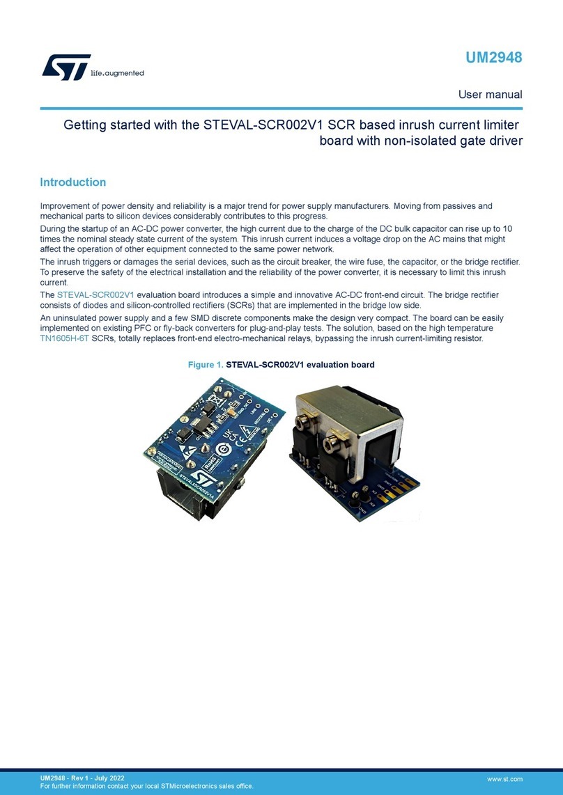
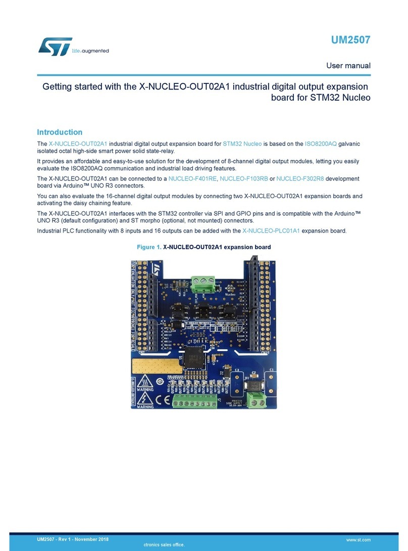
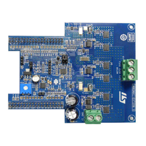
ST X-NUCLEO-SNK1M1 User manual

Introduction
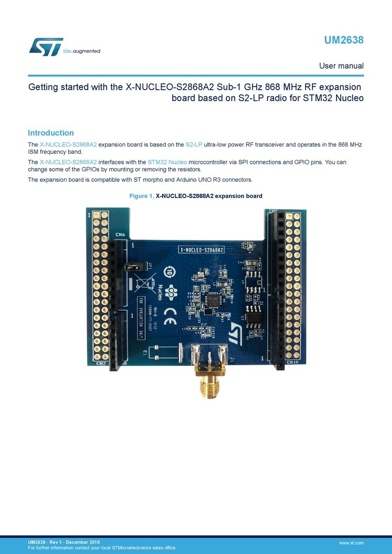
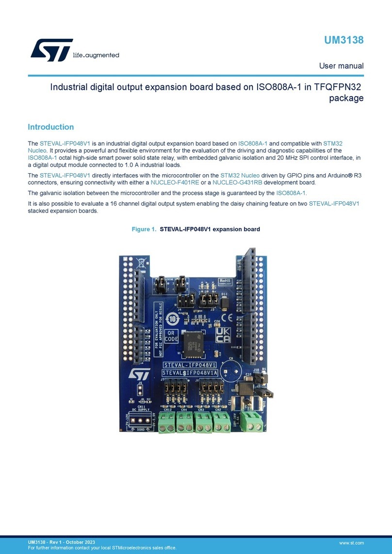
The X-NUCLEO-SNK1M1 expansion board allows evaluating the features of TCPP01-M12 and the USB Type-C® overvoltage
protection for VBUS and CC lines suitable for Sink applications.
The expansion board is designed to be stacked on top of any STM32 Nucleo-64 development board exploiting the
characteristics of the USB Type-C® and Power Delivery (UCPD) peripheral embedded in their microcontrollers.
It can also be stacked on other STM32 Nucleo development boards not supporting the UCPD peripheral to demonstrate the
USB Type-C® basic operations (attach, detach and power supply current capability recognition).
The X-NUCLEO-SNK1M1 provides an effective demonstration of the dead battery operation, thanks to the integrated
ST715PU33R LDO linear regulator that supplies the connected STM32 Nucleo development board when a Source is attached
via a USB Type-C® connector.
The X-NUCLEO-SNK1M1 is compliant with the latest USB Type-C® and Power Delivery specifications and is also USB-IF
certified as a 100 W solution supporting Programmable Power Supply (PPS) function.
The companion software package (X-CUBE-TCPP) contains the application examples for development boards embedding
UCPD-based microcontrollers (NUCLEO-G071RB, NUCLEO-G474RE and NUCLEO-G0B1RE) and for non-UCPD ones
(NUCLEO-L412RB-P).
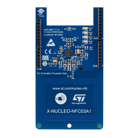
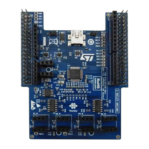
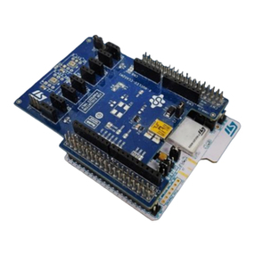
Figure 1. X-NUCLEO-SNK1M1 expansion board
Note: Before running any demo, set CC1 J1, CC2 J2, JP3 and JP4 jumpers according to the configuration described in
Section 1.3 Demo application setup.
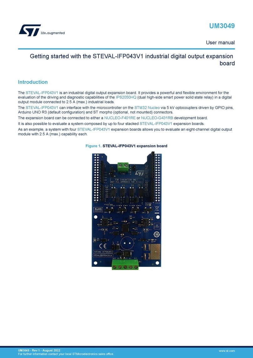
Getting started with the X-NUCLEO-SNK1M1 USB Type-C® Power Delivery Sink
expansion board based on TCPP01-M12 for STM32 Nucleo
UM2773
User manual
UM2773 - Rev 6 - August 2022
For further information contact your local STMicroelectronics sales office.
www.st.com

1Getting started
1.1 Overview
The X-NUCLEO-SNK1M1 expansion board features:
•On-board TCPP01-M12 protection for USB Type-C® and PD Sink applications
• Compliant with the latest USB Type-C® and Power Delivery specification, including the Programmable
Power Supply (PPS) feature
• USB-IF certified (Test ID certification: 5205)
• 100 W-rated solution
• 6 V overvoltage protection (OVP) on CC lines against short-to-VBUS when the connector is unplugged
• Up to 22 V adjustable overvoltage protection (OVP) on VBUS line against charger failure
• Surge protection (8/20 µs) and system-level ESD protection on VBUS
• Common mode filter and ESD protection on USB 2.0 High Speed data lines
• System level ESD protection on CC lines as per IEC61000-4-2 level 4 (±8 kV contact discharge)
• Low power mode for battery operation allowing zero current consumption when no cable is attached
• Integrated dead battery management when the device battery is fully depleted
• Overtemperature protection (OTP)
• RoHS compliant
1.2 Hardware architecture
The X-NUCLEO-SNK1M1 expansion board is designed to be used with any STM32 Nucleo-64 development
board embedding the UCPD peripheral (mainly NUCLEO-G071RB, NUCLEO-G474RE and NUCLEO-G0B1RE)
and also with the ones not supporting the UCPD peripheral.
Note: The compliance with the USB Type-C® and Power Delivery specification is guaranteed only for the STM32
Nucleo development boards embedding the microcontrollers (STM32G071RB and STM32G474RE) with a
UCPD peripheral.
When stacked with a non-UCPD STM32 Nucleo development board, the X-NUCLEO-SNK1M1 can still
demonstrate some USB Type-C® basic operations like ATTACH/DETACH recognition and identification of source
current capability.
Moreover, two couples of resistances, used as solder bridge selectors, allow exploiting the USB2.0 peripheral.
The expansion board must be plugged on the matching pins of the development board CN7 and CN10 ST
morpho connectors.
When plugged onto an STM32 Nucleo development board, the expansion board can be supplied in two different
ways:
• by the STM32 Nucleo ST-LINK supply using the development board internal LDO
• by the VBUS provided when a Source is plugged into the CN1 USB Type-C® connector and thanks to the
integrated ST715PU33R LDO linear regulator (U2) that supplies the entire system, which supports Dead
Battery operation mode.
UM2773
Getting started
UM2773 - Rev 6 page 2/23

Figure 2. X-NUCLEO-SNK1M1 main functional blocks (top view)
1. Morpho connector (CN7)
2. Arduino connector (CN6, CN8)
3. Reset jumper (JP4)
4. LDO OUT jumper (JP3)
5. 3V3 LED (LD2)
6. VBUS LED (LD1)
7. Power connector (CN2)
8. TCPP01-M12 USB-C overvoltage protection for VBUS and CC lines (U1)
9. BAT54K Schottky diode (D2)
10. CC1 line configuration jumper (J1)
11. CC2 line configuration jumper (J2)
12. USB data setting resistor (R12)
13. ECMF02-2AMX6 common-mode filter and ESD protection for USB 2.0 and MIPI/MDDI interfaces (U3)
14. USB Type-C® connector (CN1)
15. STL11N3LLH6 N-channel 30 V, 6 mOhm typ., 11 A STripFET H6 Power MOSFET (Q1)
16. Arduino connector (CN5, CN9)
17. Morpho connector (CN10)
18. USB data setting resistor (R8, R9)
19. USB data setting resistor (R13)
12
3
4
5
6
7
89
10
11
12
13
14
16
17
18
15
19
UM2773
Hardware architecture
UM2773 - Rev 6 page 3/23

Figure 3. X-NUCLEO-SNK1M1 main functional blocks (bottom view)
1. Morpho connector (CN10)
2. ESDA25P35-1U1M TVS diode (D1)
3. OVP threshold solder bridges (SH1, SH2, SH3, SH4, SH5)
4. ST715PU33R high input voltage LDO linear regulator (U2)
5. Morpho connector (CN7)
1
2
3
4
5
1.2.1 USB Type-C® connector
The USB Type-C® receptacle (CN1) gathers the VBUS path and the main connections, such as CC lines and
USB2.0 data lines (DP
, DM), before dispatching data to the major functional blocks.
Figure 4. Type-C receptacle (CN1) and ESDA25P35-1U1M TVS diode (D1)
VBUSc
GND
GND
GND
GND
CN1
GND4
B12
WE-632723300011
RX1+
B11
RX1-
B10
VBUS4
B9
SBU2
B8
B5
D-2
D+2
CC2
B4
B3
B2
B1
GND1 A1
VBUS3
TX2-
TX2+
GND3
TX1+ A2
TX1- A3
VBUS1 A4
CC1 A5
D+1 A6
A7
A8
A9
A10
A11
A12
B6
B7
D-1
SBU1
VBUS2
RX2-
RX2+
GND2
C2
330p
D1
ESDA25P35-1U1M
C1
330p
GND_C GND_C
VBUSc
CC1c
DM DP
DP DM
CC2c
VBUSc
GND_C GND_C
Note: VBUS path capacitive value should be included between 1 µF and 10 µF for a USBPD SINK port design.
An ESDA25P35-1U1M TVS diode has been integrated to protect the VBUS power line and, consequently, the
entire system against EOS and ESD transients when a Source is connected through the USB Type-C® cable.
UM2773
Hardware architecture
UM2773 - Rev 6 page 4/23

1.2.2 TCPP01-M12 USB Type-C® protection and VBUS overvoltage protection setup
TCPP01-M12 (U1) protects the CC1 and CC2 pins of the USB Type-C® and PD controller sink against
overvoltage in case a short-circuit event with the VBUS occurs during the attach or detach operation with a
defective tool.
The protection is implemented by removing the USB Type-C® cable from its receptacle.
Figure 5. TCPP01-M12 protection (U1) driving the STL11N3LLH6 MOS (Q1)
Connector
side
DB/
CC1
CC2
CC1c
CC2c
VCC
FLT
VBUS
VCC
GND
GND
GND
SH1 0 N.M.
D2
R3
10k
SH5
0 N.M.
U1
TCPP01_M12
6
VBUS_CTRL
3CC1 7
CC1c
1CC2 9
CC2c
DB/
10 FLT/ 11
GND
2
GND1
13
4
SOURCE
5
GATE
8
IN_GD
VCC
12
C3
R1_22V 620
SH3 0 N.M.
Q1
6
4
2
STL11N3LLH6
1
35
7
8
10k
CC1
CC2
CC1c
CC2c
VBUS
DB/
VBUSc
VBUS_CTRL
VBUS_CTRL
Controller
side
0 N.M.
0
R1_6V 2.7k
R1_10V 1.5k
R1_13V 1.1k
R1_17V 820
BAT54K
100n
R2
TCPP01-M12 overvoltage protection (OVP) threshold setup mechanism is based on a resistive network
composed of five resistors (R1_6V, R1_10V, R1_13V, R1_17V and R1_22V) and five solder bridges (SH1, SH2,
SH3, SH4, and the SH5). Connected to the device through the BAT54K signal Schottky diode (D2), this section is
shown in the figure above (left side) and is placed at the board bottom.
On the X-NUCLEO-SNK1M1 expansion board, the 22 V OVP threshold is set by default via SH5. To change the
threshold to another value (6, 10, 13 or 17 V), remove SH5 and add a different solder bridge on the selected OVP
voltage.
When a defective power source plugged onto the Type-C connector produces a voltage higher than the selected
OVP threshold, the TCPP01-M12 OVP mechanism controls the external MOSFET Q1 and interrupts the VBUS
line.
The current X-NUCLEO-SNK1M1 setup is compliant with the USB Type-C® and Power Delivery specifications. It
is certified by USB-IF, with TID certification no. 5205.
However, some USB Type-C® adapters and equipment, which are not compliant with the specification, might
latch the solution to overvoltage when connected to it. This is due to the generation of an initial spike that is very
close to the OVP upper limit.
In such occurrences, we suggest replacing the resistance values according to the values reported in the table
below, in the “Recommended resistor” column.
Table 1. Resistor values
VBUS max Pmax Resistor reference Onboard values (mounted) Recommended values for noncompliant
adapters
6 V 15 W R1_6V 2.7 k 2.4 k
10 V 27 W R1_10V 1.5 k 1.27 k
13 V 36 W R1_13V 1.1 k 910 k
17 V 45 W R1_17V 820 k 715 k
22 V 100 W R1_22V 620 k 536 k
This new set of resistors still filters against voltage spike at startup, but do not latch the OVP.
UM2773
Hardware architecture
UM2773 - Rev 6 page 5/23

You can use several Q1 MOSFET references with various tradeoffs on the key parameters: the size for the PCB
surface, RDS(on) for the static drain-source on-resistance insertion losses and VDS for the maximum drain-source
voltage when the surge is clamped by the TVS diode (D1).
The dual Q1 MOSFET (back-to-back configuration) is required if the voltage is maintained on the consumer path
when there is no VBUS voltage.
Table 2. N-MOSFET performance tradeoff
Order code N-MOSFET Package RDS(on) typ. VDS max.
STL6N3LLH6 Single PowerFLAT 2x2 Single island 32 mΩ 30 V
STL11N3LLH6 Single PowerFLAT 3.3x3.3 Single island 8.4 mΩ 30 V
STL260N4LF7 Single PowerFLAT 5x6 Single island 1.2 mΩ 40 V
STL40DN3LLH5 Dual PowerFLAT 5x6 Dual island 20 mΩ 30 V
STL105DN4LF7AG Dual PowerFLAT 5x6 Dual island 5.3 mΩ 40 V
1.2.3 CC lines and configuration jumpers
Two headers for jumpers (J1 and J2) have been integrated to change the CC lines paths from the TCPP01-M12
protection to the ST morpho connectors (CN7 and CN10) on the STM32 Nucleo development board, setting them
differently according to the peripheral mapping of the STM32 microcontroller.
This integration guarantees the solution flexibility support for the demo across the STM32 Nucleo-64 development
board range.
Figure 6. CC line configuration jumpers
CC1
CC2
GND
GND
R21
5.1k
0
R16 100
0R18
J4
R15
0R19
R17
5.1k
0R22
J3
R20 100
J1
1
JUMPER
2
3
J2
1
JUMPER
2
3
CC1_G4
CC1_G0
CC2_G4
CC1_no_UCPD
CC2_no_UCPD
CC2_G0
R14
0
Jumper-Female
Jumper-Female
The table below shows the jumper settings to configure the X-NUCLEO-SNK1M1 to work with the STM32 Nucleo
development boards embedding the UCPD peripherals (NUCLEO-G071RB, NUCLEO-G474RE and NUCLEO-
G0B1RE) as well as with other STM32 Nucleo-64 boards (NUCLEO-L412RB-P) implementing the USB Type-C®
attach-detach recognition mechanism.
UM2773
Hardware architecture
UM2773 - Rev 6 page 6/23

Table 3. J1 and J2 CC lines configuration setting jumpers
Compatible STM32 Nucleo
boards
Jumpers
CC1 - J1 CC2 -J2
Any STM32 Nucleo-64
development board with
UCPD (NUCLEO-G071RB,
NUCLEO-G474RE and NUCLEO-
G0B1RE)
Any STM32 Nucleo-64
development board without UCPD
(NUCLEO-L412RB-P)
When both configuration jumpers (J1 and J2) are set to positions 1-2, the board is compatible with NUCLEO-
G071RB, NUCLEO-G474RE and NUCLEO-G0B1RE offering the UCPD peripheral.
This association permits to fully demonstrate the main characteristics of the USB Type-C® and Power Delivery
standards implemented by the demo application example.
When J1 and J2 are both set to positions 2-3, the X-NUCLEO-SNK1M1 can match any STM32 Nucleo-64
development board, demonstrating the basic mechanism of the Type-C specification, thanks to two pull-down
resistors (R17 and R21) connected to the pins working as CC lines, allowing the Sink USB Type-C® operations to
run with any attached Source.
1.2.4 USB 2.0 data path and configuration setting
The X-NUCLEO-SNK1M1 expansion board allows STM32 Nucleo development boards that feature a USB2.0
peripheral to expose the D+/D- lines on the USB Type-C® receptacle (CN1).
Most STM32 Nucleo-64 development boards feature this functionality on the ST morpho connector CN10-12 and
CN10-14 pins, whereas NUCLEO-L412RB-P, NUCLEO-L433RC-P, NUCLEO-L452RE-P and NUCLEO-L476RG
boards map USB2.0 data pins on CN10-33 and CN10-17 pins.
Two couples of resistances has been implemented and connected to the ECMF02-2AMX6 (U3) USB2.0 data lines
protection to extend the use of this peripheral to all the STM32 Nucleo-64 development boards.
Figure 7. USB2.0 data lines protection ECMF02-2AMX6 (U3) and resistor setup
ZDiff 90 Ohm
DP_Gx_Fx
DM_Gx_Fx
DP_Lx
DM_Lx
GND
N.M.
U3
1DP1
ECMF02_2AMX6
2DM2
3GND 4
NC
5
DM5
6
DP6
0R12
N.M.
DP
DM
R8 0
R9 0
R13 0
ZDiff 90 Ohm
UM2773
Hardware architecture
UM2773 - Rev 6 page 7/23

By default, the X-NUCLEO-SNK1M1 board mounts R8 and R9 resistors fitted to guarantee USB2.0 compatibility
to all the main microcontroller families, but, for the L4 family (NUCLEO-L412RB-P, NUCLEO-L433RC-P,
NUCLEO-L452RE-P and NUCLEO-L476RG) only, they have to be removed and replaced by R12 and R13 solder
bridges.
1.2.5 ST morpho and Arduino UNO V3 connectors
The figure below shows the X-NUCLEO-SNK1M1 expansion board ST morpho and Arduino UNO V3 connectors,
detailing the main connections, functions and configuration settings.
Figure 8. ST morpho and Arduino UNO V3 connectors
VCC FLT
VBUS
DP_Gx_Fx
DM_Gx_Fx
DP_Lx
DM_Lx
3.3V
GND
GND
GND
GND
3.3V
1 2
34
5 6
7 8
9 10
11 12
13
15 16
26
19 20
21 22
23 24
25
27 28
30
31 32
33 34
36
37 38
R6
40.2k
CN6
1
2
3
61300811821
5
6
7
8
CN9
1
2
4
5
6
7
8
R23 0
N.M.
R7
200k 0R24
CN5
1
2
4
5
6
7
8
9
CN8
1
2
3
5
6
CN7
1 2
4
5 6
7 8
9 10
11 12
13 14
15 16
17 18
23 24
25 26
27 28
31 32
33 34
35 36
D15
VDD E5V
D14
BOOT0 GND
AVDD U5V
NC/
GND
IOREF
D13
D12
RESET NRST
+3V3
D11
+5V
CC1_G4
D10
FLT_IN
GND GND
D9 GND
D6
DB_OUT
CC2_G0
A0
A1
D4
A2 AGND
A3
D2
A4
D1
A5
D15
NC/ D14
IOREF AVDD
RESET GND
+3V3 D13
+5V D12
GND D11
GND D10
VIN
D8
D7
A0
D5
A2
A3
D3
A4
A5
D1
D0
ADC_VBUS
VCC_OUT
FLT_IN
VCC_OUT
3
19
21
29
37
20
22
30
38
GND
VIN
A0
A2
A5
CC1_no_UCPD
CC2_no_UCPD
ADC_VBUS
R27
0
4
ESQ-119-24-T-D
A1
A2
A4
4
61300811821
61300811821
61300811821
3
D9
D6
3
ESQ-119-24-T-D
14
17 18
29
35
CN10
R22 0
In addition to the main functions related to the USB Type-C® and Power Delivery specification:
•an ADC channel can be used to monitor the VBUS voltage (ADC_VBUS)
• a supply option path allows supplying the TCPP01-M12 either via the 3.3 V provided by the STM32 Nucleo
development board or via a GPIO on the ST morpho connector (CN7-1). You can select the path through
R23 and R24 resistances. This option, combined with the TCPP01-M12 low consumption, is useful for
battery-powered devices as the TCPP01-M12 can be powered only when an attachment is detected (low-
power mode)
• the TCPP01-M12 fault report pin (open drain) is connected to the ST morpho connector pin (CN10 – 18) to
be monitored by the STM32 microcontroller (FLT – FLT_IN path)
1.2.6 Indication LEDs
Two LEDs mounted on the X-NUCLEO-SNK1M1 top side indicate the supply status of the expansion board and
the stacked STM32 Nucleo development board:
•the red LED (LD1) turns ON when a source application board is plugged to the X-NUCLEO-SNK1M1 CN1
connector and the USB Type-C® VBUS voltage is present;
• the green LED (LD2) indicates that the 3.3 V is present and is supplying the STM32 Nucleo microcontroller
development board.
UM2773
Hardware architecture
UM2773 - Rev 6 page 8/23

Figure 9. Indication LEDs
3.3V
GND GND
R5
LD1
AC
150060RS75000
3.9k
LD2
AC
VBUS
Red LED
Green LED
3.3V
VBus
R4
150060GS75000
1k
1.2.7 Dead battery mode configuration jumpers and internal LDO
Thanks to the dead battery feature, described by the USB Power Delivery specification and implemented by the
X-NUCLEO-SNK1M1, it is possible to directly power the system through the VBUS provided by a Source, as an
alternative mode to the standard supply through the STM32 Nucleo ST-LINK.
Note: Before configuring the X-NUCLEO-SNK1M1 to operate in dead battery mode, check whether the supply
selection jumpers on the STM32 Nucleo board have been removed:
• on the NUCLEO-G071RB and the NUCLEO-G0B1RE, remove the jumper from JP2 header
• on the NUCLEO-G474RE, remove the jumper from JP5 header 5V_SEL
• on the NUCLEO-L412RB-P, remove the jumper from JP5 header
Figure 10. Dead battery mode circuitry
DB/
3.3V
GND
3.3V
CN10
C6
1u
U2
NC
2
ST715PU33R
GND
4
1
Vin 3
8
6
FB
5
7
9
EXP
J5
J6
N.M.
C5
220n
VBUS
LDO_OUT
LDO_OUT
NRST
DB_OUT
Jumper-Female
JP3 JUMPER-con2 strip-male
JP4
JUMPER-con2 strip-male
Jumper-Female
R25 0
R26 0
To select the dead battery operation mode on the X-NUCLEO-SNK1M1, JP3 and JP4 jumpers must be fit.
Table 4. JP3 and JP4 power mode selection jumpers
Power mode
Jumpers
JP3 (LDO_OUT) JP4 (RESET)
ST-LINK powered mode
(open) (open)
UM2773
Hardware architecture
UM2773 - Rev 6 page 9/23

Power mode
Jumpers
JP3 (LDO_OUT) JP4 (RESET)
Dead battery mode
(fit) (fit)
JP3 jumper connects the VBUS path from the Type-C connector to the LDO (U2) which is connected to the STM32
Nucleo development board 3.3 V path and can power the entire solution.
When fitted, JP5 jumper forces the STM32 I/O negative reset to level 1. It must be connected when the STM32 is
powered by the X-NUCLEO-SNK1M1.
By default, the TCPP01-M12 dead battery option has been set to be driven by an STM32 microcontroller pin
through R26 solder bridge, thus removing the TCPP01-M12 dead battery clamp when GPIO is connected on ST
morpho connector (CN10-24). The alternative operating mode is to fit the TCPP01-M12 dead battery option to
3V3 through the R25 mounting solder bridge (consequently, R26 must be not fitted).
In the application firmware package, this option has been included in the firmware examples where a GPIO (ST
morpho CN10-24) properly drives the dead battery option.
1.2.8 Power connector
CN2 power connector can be used to connect a load and monitor the VBUS voltage level negotiated by the system
with a Source attached to CN1 USB Type-C® connector.
Figure 11. CN2 power connector
CN2
1
2
VBUS
GND
691210910002
Note: To monitor the output voltage, an appropriate resistance has to be connected to the X-NUCLEO-SNK1M1 CN2.
1.3 Demo application setup
The X-NUCLEO-SNK1M1 expansion board flexibility permits to demonstrate the TCPP01-M12 protection features
and capabilities with a wide range of STM32 Nucleo development boards.
The X-CUBE-TCPP companion software package contains specific application examples for the STM32 Nucleo
embedding the USB Type-C® and Power Delivery management (NUCLEO-G071RB, NUCLEO-G474RE and
NUCLEO-G0B1RE) and, for the ones without the UCPD peripheral, the package demonstrates how to comply
with basic USB Type-C® operations (NUCLEO-L412RB-P).
1.3.1 Programming and debugging
Once the X-NUCLEO-SNK1M1 expansion board has been connected to a NUCLEO-G071RB, NUCLEO-
G474RE, NUCLEO-G0B1RE or NUCLEO-L412RB-P, to program and debug, the STM32 Nucleo development
board has to be connected to a laptop by the embedded USB ST-LINK connector (CN2) to supply the solution
and program the firmware example in the application microcontroller.
UM2773
Demo application setup
UM2773 - Rev 6 page 10/23

Note: Set the jumpers as follows:
•On the STM32 Nucleo development board, ensure the 5 V selection jumper fits with the 5 V ST-LINK
header (JP5 on NUCLEO-G474RE and NUCLEO-L412RB-P, JP2 on NUCLEO-G071RB and NUCLEO-
G0B1RE)
• On the X-NUCLEO-SNK1M1 expansion board:
– remove LDO OUT jumper (JP3)
– remove NRST jumper (JP4)
Note: The X-CUBE-TCPP MCU firmware applications are designed to select the highest and closest power profile
exposed by the Source, after the explicit contract negotiation.
1.3.1.1 Running the demo application with NUCLEO-G071RB or NUCLEO-G0B1RE development board
The NUCLEO-G071RB development board embeds the STM32G071RB microcontroller with the UCPD
peripheral. To run the application demo with the NUCLEO-G071RB, powering the system via ST-LINK micro-USB
connector, follow the procedure below.
Step 1. Check the jumper is closed on the development board JP2 header, STLK 1-2 pins.
Step 2. On the X-NUCLEO-SNK1M1 expansion board, fit CC1 JP1 and CC2 JP2 jumpers on position 1-2.
Step 3. Plug the expansion board on top of the STM32 Nucleo and leave JP3 and JP4 headers open.
Step 4. Connect the NUCLEO-G071RB or NUCLEO-G0B1RE micro-USB connector (CN1) to the PC/laptop.
The board appears as a virtual disk (NODE_G071RB).
Step 5. Program the STM32G071RB by dragging and dropping the binary file corresponding to the board
(G0_SNK1M1_Consumer.bin) to the virtual disk.
STM32 Nucleo LD1 LED blinks red and green for few seconds. When the LED stops blinking, the
programming operation is complete and the demo is ready.
Step 6. Plug a Source application board on the X-NUCLEO-SNK1M1 expansion board CN1 connector through
a USB Type-C® cable and refer to the following LED operation description to identify the application
results:
–NUCLEO-G071RB/NUCLEO-G0B1RE LD3 LED is ON when the board is supplied by the ST-
LINK micro-USB connector (CN1)
–X-NUCLEO-SNK1M1 LD2 LED is ON when the 3V3 voltage is provided to the expansion board
by the STM32 Nucleo
–X-NUCLEO-SNK1M1 LD1 LED is ON when a Source is connected to the USB Type-C® CN1
connector and the VBUS is provided
–NUCLEO-G071RB/NUCLEO-G0B1RE LD4 LED:
◦ blinks once every 2 seconds when USB default (up to 500 mA) is identified
◦ blinks twice every 2 seconds when a Source USB Type-C® 1.5 A current capability is
identified;
◦ blinks 3 times every 2 seconds when a Source USB Type-C® 3 A current capability is
identified;
◦ is ON when the explicit negotiation between the two contractors is reached.
1.3.1.1.1 Dead battery operation mode
Step 1. Repeat steps 1- 4 described in Section 1.3.1.1
Step 2. Disconnect the micro-USB cable from NUCLEO-G071RB/NUCLEO-G0B1RE CN1.
Step 3. Remove the power selection jumper from the JP2 header on NUCLEO-G071RB/NUCLEO-G0B1RE
development board (previously set on STLK 1-2 pins) and leave it fully open.
Step 4. On the X-NUCLEO-SNK1M1, set LDO OUT jumper (JP3) and NRST jumper (JP4).
Step 5. Plug a Source board to X-NUCLEO-SNK1M1 CN1 connector through a USB Type-C® cable.
The provided VBUS supplies the Sink solution while the LEDs define the status as previously described.
UM2773
Demo application setup
UM2773 - Rev 6 page 11/23

1.3.1.2 Running the demo application with NUCLEO-G474RE development board
The NUCLEO-G474RE development board embeds the STM32G474RE microcontroller with the UCPD and
USB2.0 data peripherals. To run the application demo with the NUCLEO-G474RE, powering the system via
ST-LINK micro-USB connector, follow the procedure below.
Step 1. Check the jumper is closed on the development board JP5 header, 5V_STLK 1-2 pins.
Step 2. On the X-NUCLEO-SNK1M1 expansion board, fit CC1 JP1 and CC2 JP2 jumpers on position 1-2.
Step 3. Plug the expansion board on top of the STM32 Nucleo and leave JP3 and JP4 headers open.
Step 4. Connect the NUCLEO-G474RE micro-USB connector (CN1) to the PC/laptop.
The board appears as a virtual disk (NODE_G474RE).
Step 5. Program the STM32G474RE by dragging and dropping the binary file corresponding to the board
(G4_SNK1M1_Consumer.bin) to the virtual disk.
STM32 Nucleo LD1 LED blinks red and green for few seconds. When the LED stops blinking, the
programming operation is complete and the demo is ready.
Step 6. Plug a Source application board on the X-NUCLEO-SNK1M1 expansion board CN1 connector through
a USB Type-C® cable and refer to the following LED operation description to identify the application
results:
–NUCLEO-G474RE LD3 LED is ON when the board is supplied by the ST-LINK micro-USB
connector (CN1)
–X-NUCLEO-SNK1M1 LD2 LED is ON when the 3V3 voltage is provided to the expansion board
by the STM32 Nucleo
–X-NUCLEO-SNK1M1 LD1 LED is ON when a Source is connected to the USB Type-C® CN1
connector and the VBUS is provided
–NUCLEO-G474RE LD2 LED:
◦ blinks once every 2 seconds when USB default (up to 500 mA) is identified
◦ blinks twice every 2 seconds when a Source USB Type-C® 1.5 A current capability is
identified;
◦ blinks 3 times every 2 seconds when a Source USB Type-C® 3 A current capability is
identified;
◦ blinks 4 times every 2 seconds when the explicit negotiation between the two contractors is
reached;
◦ turns ON when the explicit negotiation between the two contractors is reached and the
USB2.0 data connection is established.
1.3.1.2.1 Dead battery operation mode
Step 1. Repeat steps 1- 4 described in Section 1.3.1.2
Step 2. Disconnect the micro-USB cable from NUCLEO-G474RE CN1.
Step 3. Remove the power selection jumper from the JP2 header on NUCLEO-G474RE development board
(previously set on STLK 1-2 pins) and leave it fully open.
Step 4. Set JP8 jumper on 2-3 pins.
Step 5. On the X-NUCLEO-SNK1M1, set LDO OUT jumper (JP3) and NRST jumper (JP4).
Step 6. Plug a Source board to X-NUCLEO-SNK1M1 CN1 connector through a USB Type-C® cable.
The provided VBUS supplies the Sink solution while the LEDs define the status as previously described.
1.3.1.3 Running the demo application with NUCLEO-L412RB-P development board
The NUCLEO-L412RB-P development board embeds the STM32L412RB microcontroller which includes the
USB2.0 data peripheral only. The application example demonstrates that the TCPP01-M12 protection can be
matched with microcontrollers which does not include the UCPD peripheral to implement a USB Type-C® Sink
port only, thus exploiting the microcontroller ADC peripherals to monitor the current capabilities of the Source. To
run the application demo with the NUCLEO-L412RB-P, powering the system via ST-LINK micro-USB connector,
follow the procedure below.
UM2773
Demo application setup
UM2773 - Rev 6 page 12/23

Step 1. Check the jumper is closed on the development board JP5 header, 5V_STLK 1-2 pins.
Step 2. On the X-NUCLEO-SNK1M1 expansion board, fit CC1 JP1 and CC2 JP2 jumpers on position 1-2.
Step 3. Plug the expansion board on top of the STM32 Nucleo and leave JP3 and JP4 headers open.
Step 4. Connect the NUCLEO-L412RB-P micro-USB connector (CN1) to the PC/laptop.
The board appears as a virtual disk (NODE_L412RB).
Step 5. Program the STM32L412RB by dragging and dropping the binary file corresponding to the board
(SNK1M1_Consumer_TypeC_Only.bin) to the virtual disk.
STM32 Nucleo LD1 LED blinks red and green for few seconds. When the LED stops blinking, the
programming operation is complete and the demo is ready.
Step 6. Plug a Source application board on the X-NUCLEO-SNK1M1 expansion board CN1 connector through
a USB Type-C® cable and refer to the following LED operation description to identify the application
results:
–NUCLEO-L412RB-P LD3 LED is ON when the board is supplied by the ST-LINK micro-USB
connector (CN1)
–X-NUCLEO-SNK1M1 LD2 LED is ON when the 3V3 voltage is provided to the expansion board
by the STM32 Nucleo
–X-NUCLEO-SNK1M1 LD1 LED is ON when a Source is connected to the USB Type-C® CN1
connector and the VBUS is provided
–NUCLEO-L412RB-P LD2 LED:
◦ blinks once every 2 seconds when USB default is identified
◦ blinks twice every 2 seconds when a Source USB Type-C® 1.5 A current capability is
identified;
◦ blinks 3 times every 2 seconds when a Source USB Type-C® 3 A current capability is
identified.
1.3.1.3.1 Dead battery operation mode
Step 1. Repeat steps 1- 4 described in Section 1.3.1.3
Step 2. Disconnect the micro-USB cable from NUCLEO-L412RB-P CN1.
Step 3. Remove the power selection jumper from the JP2 header on NUCLEO-L412RB-P development board
(previously set on STLK 1-2 pins) and leave it fully open.
Step 4. On the X-NUCLEO-SNK1M1, set LDO OUT jumper (JP3) and NRST jumper (JP4).
Step 5. Plug a Source board to X-NUCLEO-SNK1M1 CN1 connector through a USB Type-C® cable.
The provided VBUS supplies the Sink solution while the LEDs define the status as previously described.
Note: The firmware application example designed for the NUCLEO-L412RB-P embeds the USB2.0 driver
which can start the USB enumeration when the board is connected to a laptop or a PC. To test this
functionality, R8 and R9 solder bridges have to be mounted while R12 and R13 have to be mounted.
UM2773
Demo application setup
UM2773 - Rev 6 page 13/23

2Schematic diagrams
Figure 12. X-NUCLEO-SNK1M1 circuit schematic (1 of 2)
Interface
Configuration
VCC
FLT
DB/
VBUS
CC1
CC2
DP_Gx_Fx
DM_Gx_Fx
DP_Lx
DM_Lx
3.3V
3.3V
GND
GND
GND
GND
GND
GND
GND
3.3V
3.3V
CN10
1 2
3
ESQ-119-24-T-D
4
5 6
7 8
9 10
11 12
For the STM32 Nucleo families embedding
L412, L433, L452 and L476, the
USB DM pin coexists with STMG4
CC1 pin.
To exploit the USB functionality
with these L4 families, the
solder bridges R12, R13 must be
fit and removed the R8 and R9.
13 14
15 16
17 18
19 20
21 22
23 24
25 26
27 28
29 30
31 32
33 34
35 36
37 38
R21
5.1k
0R14
JP3 JUMPER-con2-strip-male
R16 100
C6
1u 0R26
0R18
U2
NC 2
ST715PU33R
GND
4
1Vin 3
NC1
8
OUT 6
NC2
FB
5
7
NC3 9
EXP
R6
40.2k
J4
CN6
Jumper-Female
1
2
3
61300811821
4
5
6
7
8
J5
CN9
Jumper-Female
1
2
3
61300811821
4
5
6
7
8
0R23
N.M.
J6
0R25
Jumper-Female
N.M.
0R15
R7
200k
C5
220n
0R19
R17
5.1k
0R22
0R24
J3
R20 100
Jumper-Female
0
R27
J1
1
JUMPER
2
3
CN5
1
2
3
61301011821
4
5
6
7
8
9
10
JP4
CN8
JUMPER-con2-strip-male
1
2
3
61300611821
4
5
6
CN7
1 2
3
ESQ-119-24-T-D
4
5 6
7 8
9 10
11 12
13 14
15 16
17 18
19 20
21 22
23 24
25 26
27 28
29 30
31 32
33 34
35 36
37 38
J2
1
JUMPER
2
3
D15
VDD E5V
D14
BOOT0 GND
AVDD U5V
NC/
GND
IOREF
D13
D12
RESET NRST
+3V3
D11
+5V
CC1_G4 D10 FLT_IN
GND GND
D9 GND
GND
D8
VIN
CC1_G0 D7
D6
DB_OUT
CC2_G0
A0 CC1_no_UCPD
CC2_G4 D5
A1
D4
A2
CC2_no_UCPD D3 AGND
A3VLCD/VBAT
D2
ADC_VBUS
A4
D1
A5
D0
D15
NC/ D14
IOREF AVDD
RESET GND
+3V3 D13
+5V D12
GND D11
GND D10
VIN D9
D8
D7
A0
D6
A1
D5
A2
D4
A3
D3
A4
D2
A5
D1
D0
VBUS
LDO_OUT
ADC_VBUS
FLT_IN
LDO_OUT
NRST
CC1_G4
CC1_G0
CC2_G4
CC1_no_UCPD
CC2_no_UCPD
VCC_OUT
DB_OUT
CC2_G0
VCC_OUT
UM2773 - Rev 6 page 14/23
UM2773
Schematic diagrams

Figure 13. X-NUCLEO-SNK1M1 circuit schematic (2 of 2)
3. 3V VBus
USB TYPE-C® RECEPTACLE
ZDi f f 90 Ohm ZDi f f 90 Ohm
2
DB/
CC1
CC2
DP_Gx_Fx
DM_Gx_Fx
VBUSc
DP_Lx
DM_Lx
CC1c
CC2c
VCC
FLT
VBUS
VCC
GND
GND
GND
GND
GND
GND
GND GND
GND
GND
GND
3.3V
CN1
GND4
B12
WE-632723300011
RX1+
B11
RX1-
B10
VBUS4
B9
SBU2
B8
B5
D-2
D+2
CC2
B4
B3
B2
B1
GND1 A1
VBUS3
TX2-
TX2+
GND3
TX1+ A2
TX1- A3
VBUS1 A4
CC1 A5
D+1 A6
A7
A8
A9
A10
A11
A12
B6
B7
D-1
SBU1
VBUS2
RX2-
RX2+
GND2
SH1 0 N.M.
D2
BAT54K
R9 0
R3
10k
R1_17V 820
C2
330p
R1_6V 2.7k
0
SH5
D1
SH4
ESDA25P35-1U1M
0 N.M.
0R13
N.M.
CN2
1
2
691210910002
C1
330p
SH2 0 N.M.
U1
TCPP01_M12
6
VBUS_CTRL
3CC1 7
CC1c
1CC2 9
CC2c
DB/
10 FLT/ 11
GND
2
GND1
13
4
SOURCE
5
GATE
8
IN_GD
VCC
12
C3
100n
R8 0
R1_22V 620
R5
1k
R1_10V 1.5k
SH3 0 N.M.
Q1
6
4
2
STL11N3LLH6
1
35
7
8
LD1
AC
150060RS75000
U3
1DP1
ECMF02_2AMX6
2DM2
3GND 4
NC
5
DM5
6
DP6
R4
R1_13V 1.1k
3.9k
0R12
N.M.
LD
AC
R2
150060GS75000
10k
CC1
CC2
CC1c
CC2c
VBUS
DB/
GND_C GND_C
VBUSc
CC1c
DM DP
DP DM
CC2c
VBUSc
GND_C GND_C
VBUSc
VBUS_CTRL
VBUS_CTRL
DP
DM
VBUS
VBUS
side
Connector
side
Controller
Gr een LED Red LED
UM2773 - Rev 6 page 15/23
UM2773
Schematic diagrams

3Bill of materials
Table 5. X-NUCLEO-SNK1M1 bill of materials
Item Q.ty Ref. Part/value Description Manufacturer Order code
1 2 C1, C2
330 p, 0402
(1005 Metric), 50
Vdc V, ±10 %,
SMD 0402 X7R
Ceramic
capacitors
Wurth Electronics
Inc. 885012205058
2 1 C3
100 n, 0402
(1005 Metric),
50Vdc V, ±10 %,
SMD 0402 X7R
Ceramic
capacitor TDK C1005X7R1H104K050
BB
3 1 C5
220n, 0402 (1005
Metric), 35Vdc V,
±10 %, SMD
0402 X7R
Ceramic
capacitor
Murata
Electronics
GRM155C8YA224ME0
1D
4 1 C6
1 µF, 0402 (1005
Metric), 6Vdc V,
±10 %, SMD
0402 X5R
Ceramic
capacitor Kemet C0402C105K8PAC7411
5 1 CN1 WE-6327233000
11, THT/SM
USB 3.1
Type-C
receptacle
Wurth Electronics
Inc. 632723300011
6 1 CN2 691210910002,
2.54 mm Terminal block Wurth Electronics
Inc. 691210910002
7 1 CN5
61301011821, 10
pos., 0.1, gold
PCB
Connector
receptacle
Wurth Electronics
Inc. 61301011821
8 2 CN6, CN9
61300811821, 8
pos., 0.1, gold
PCB
Connector
receptacles
Wurth Electronics
Inc. 61300811821
9 2 CN7, CN10
ESQ-119-24-T-D,
38 pos., 0.1, gold
PCB
Connector
receptacles Samtec Inc. ESQ-119-24-T-D
10 1 CN8
61300611821, 6
pos., 0.1, gold
PCB
Connector
receptacle
Wurth Electronics
Inc. 61300611821
11 1 D1
ESDA25P35-1U1
M, 2-UDFN, 1400
W (1.4 kW)
High power
transient
voltage
suppressor
ST ESDA25P35-1U1M
12 1 D2
BAT54K, SC-79,
SOD-523, 900
mV @ 100 mA V,
300mA (DC) A
General
purpose
Schottky
diode
ST BAT54KFILM
13 2 J1, J2 Jumper, 3 pos. Connector
header AMTEK PH1S25-1x03GB6/3-L
14 1
J3 FIT ON
PIN 1-2 OF
J1
Jumper,female Connector
jumper AMTEK MJ1B-AGB-L
15 1
J4, FIT ON
PIN 1-2 OF
J2
Jumper,female Connector
jumper AMTEK MJ1B-AGB-L
16 2
J5, J6
PROVIDE
BUT NOT
ASSEMBLY
Jumper,female Connector
jumpers AMTEK MJ1B-AGB-L
UM2773
Bill of materials
UM2773 - Rev 6 page 16/23

Item Q.ty Ref. Part/value Description Manufacturer Order code
17 2 JP3, JP4 Jumpers, con2-
strip-male
Connector
jumpers AMTEK PH1S25-1x02GB6/3-L
18 1 LD1
150060RS75000,
0603 (1608
Metric), 20 m A
Red LED Wurth Electronics
Inc. 150060RS75000
19 1 LD2
150060GS75000,
0603 (1608
Metric), 20 m A
Green LED Wurth Electronics
Inc. 150060GS75000
20 1 Q1 STL11N3LLH6,
8-PowerVDFN
STripFET H6
Power
MOSFET in a
PowerFLAT
3.3 x 3.3
package
ST STL11N3LLH6
21 2 R2, R3
10 k, 0402 (1005
Metric), 0.063W,
1/16 W, ±1 %
Chip resistors Yageo RC0402FR-0710KL
22 1 R4
3.9 k, 0402 (1005
Metric), 0.063W,
1/16 W, ± 0.1 %
Chip resistor Vishay CRCW04023K90FKED
23 1 R5
1k, 0402 (1005
Metric), 0.063W,
1/16 W, ±1 %
Chip resistor Vishay CRCW04021K00FKED
24 1 R6
40.2 k, 0402
(1005 Metric),
0.063 W, 1/16 W,
±1 %
Chip resistor Vishay CRCW040240K2FKED
25 1 R7
200 k, 0402
(1005 Metric),
0.063W, 1/16 W,
±1 %
Resistor Vishay CRCW0402200KFKED
C
27 10
R8, R9, R14,
R15, R18,
R19, R22,
R24, R26,
R27
0, 0805 (2012
Metric), 1/8 W Resistors Yageo RC0805JR-070RL
28 4 R12,R13,
R23, R25
0805 (2012
Metric), 0.125 W,
1/8 W
Resistors (not
mounted) Yageo RC0805JR-070RL
29 2 R17, R21
5.1 k, 0402 (1005
Metric), 1/16 W,
±1 %
Chip resistors Vishay CRCW04025K10FKED
30 1 R1_10V
1.5 k, 0402 (1005
Metric), 1/4 W, ±1
%
Chip resistor Yageo RC0402FR-071K5L
31 1 R1_13V
1.1 k, 0402 (1005
Metric), 1/4 W, ±1
%
Chip resistor Multicomp MCWR04X1101FTL
32 1 R1_17V
820, 0402 (1005
Metric), 1/4 W, ±1
%
Chip resistor Vishay CRCW0402820RFKED
33 1 R1_22V
620, 0402 (1005
Metric), 1/16 W,
±1 %
Chip resistor Yageo RC0402FR-07620RL
34 1 R1_6V
2.7 k, 0402 (1005
Metric), 1/4 W, ±1
%
Chip resistor Yageo RC0402FR-072K7L
UM2773
Bill of materials
UM2773 - Rev 6 page 17/23

Item Q.ty Ref. Part/value Description Manufacturer Order code
35 4 SH1, SH2,
SH3, SH4
0, 0805-Solder
Bridge
Jumpers (not
mounted) Any Any
36 1 SH5 0, 0805-Solder
Bridge Jumper Any Any
37 1 U1 TCPP01-M12,
3X3X1 mm,
Overvoltage
protection for
USB-C or
Power
Delivery
ST TCPP01-M12
38 1 U2
ST715PU33R, 8-
VDFN Exposed
Pad
High input
voltage - 85
mA LDO
linear
regulator
ST ST715PU33R
39 1 U3
ECMF02_2AMX6
, 6-UFQFN, 200
mA
Common-
mode filter
and ESD
protection for
USB 2.0 and
MIPI/MDDI
interfaces
ST ECMF02-2AMX6
40 1 PCB, 72.6x58.6
mm
FR4 Standard
72.6x58.6x1.5
5 mm
Massive PCB
Technologies LTD
PROT-X-NUCLEO-
SNK1M1-ver.2
(0EC0C1)
UM2773
Bill of materials
UM2773 - Rev 6 page 18/23

Revision history
Table 6. Document revision history
Date Version Changes
15-Mar-2021 1 Initial release.
15-Apr-2021 2 Added NUCLEO-G0B1RE development board compatibility information.
10-May-2021 3 Updated Section 1.2.1 Type-C connector and Section 1.3.1.2.1 Dead battery operation mode.
02-Feb-2022 4 Updated Section 1.2.2 TCPP01-M12 USB Type-C™ protection and VBUS overvoltage protection
setup.
01-Mar-2022 5
Updated Section 1.2 Hardware architecture, Section 1.2.7 Dead battery mode configuration
jumpers and internal LDO, Section 1.3.1.1 Running the demo application with NUCLEO-G071RB
or NUCLEO-G0B1RE development board, Section 1.3.1.2 Running the demo application with
NUCLEO-G474RE development board, Section 1.3.1.3 Running the demo application with NUCLEO-
L412RB-P development board, and Section 2 Schematic diagrams.
02-Aug-2022 6 Updated Section 1.2.2 TCPP01-M12 USB Type-C® protection and VBUS overvoltage protection
setup and Section 2 Schematic diagrams.
UM2773
UM2773 - Rev 6 page 19/23

Contents
1Getting started ....................................................................2
1.1 Overview .....................................................................2
1.2 Hardware architecture ..........................................................2
1.2.1 USB Type-C® connector...................................................4
1.2.2 TCPP01-M12 USB Type-C® protection and VBUS overvoltage protection setup .........5
1.2.3 CC lines and configuration jumpers...........................................6
1.2.4 USB 2.0 data path and configuration setting ....................................7
1.2.5 ST morpho and Arduino UNO V3 connectors ...................................8
1.2.6 Indication LEDs..........................................................8
1.2.7 Dead battery mode configuration jumpers and internal LDO ........................9
1.2.8 Power connector ........................................................10
1.3 Demo application setup ........................................................10
1.3.1 Programming and debugging ..............................................10
2Schematic diagrams ..............................................................14
3Bill of materials...................................................................16
Revision history .......................................................................19
List of tables ..........................................................................21
List of figures..........................................................................22
UM2773
Contents
UM2773 - Rev 6 page 20/23
Other manuals for X-NUCLEO-SNK1M1
1
Table of contents
Other ST Computer Hardware manuals

ST
ST X-LINUX-NFC5 User manual

ST
ST STM32F405 Series User manual

ST
ST ST10R272L User manual

ST
ST STEVAL-OET005 User manual

ST
ST X-NUCLEO-OUT01A2 User manual

ST
ST MB467 User manual

ST
ST X-NUCLEO-IHM09M1 User manual

ST
ST ST32M103 Series User manual

ST
ST STM32U5 Nucleo-64 User manual

ST
ST STM8SVLDISCOVERY Installation and operating instructions