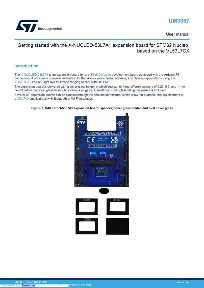
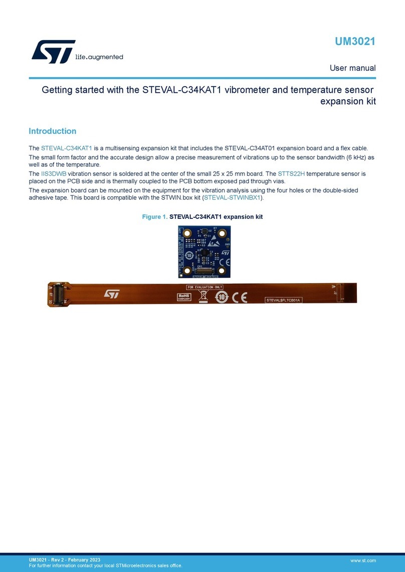
ST M41ST85W User manual

October 2011 Doc ID 7531 Rev 11 1/43
1
M41ST85W
3.0/3.3 V I2C combination serial RTC, NVRAM
supervisor and microprocessor supervisor
Features
■Automatic battery switchover and WRITE
protect for:
– Internal serial RTC and
– External low power SRAM (LPSRAM)
■400 kHz I2C serial interface
■3.0/3.3 V operating voltage
–V
CC = 2.7 to 3.6 V
■Ultralow battery supply current of 500 nA (max)
■RoHS compliant
– Lead-free second level interconnect
Serial RTC features
■400 kHz I2C
■44 bytes of general purpose NVRAM
■Counters for:
– Seconds, minutes, hours, day, date, month,
and year
–Century
– Tenths/hundredths of seconds
– Clock calibration register allows
compensation for crystal variations over
temperature
■Programmable alarm with repeat modes
– Functions in battery back-up mode
■Power-down timestamp (HT bit)
■2.5 to 5.5 V oscillator operating voltage
Microprocessor supervisor features
■Programmable watchdog
– 62.5 ms to 128 s time-out period
■Early power-fail warning circuit (PFI/PFO) with
1.25 V precision reference
■Power-on reset/low voltage detect
– Open drain reset output
– Reset voltage, VPFD = 2.60 V (nom)
– Two reset input pins
– Watchdog can be steered to reset output
NVRAM supervisor features
■Non-volatizes external LPSRAM
– Automatically switches to back-up battery
and deselects (write-protects) external
LPSRAM via chip-enable gate
– Power-fail deselect (write protect) voltage,
VPFD = 2.60 V (nom)
– Switchover, VSO = 2.50 V (nom)
■Battery monitor (battery low flag)
Other features
■Programmable squarewave generator (1 Hz to
32 KHz)
■–40°C to +85°C operation
■Package options:
– 28-lead SNAPHAT®IC (SOH28) SNAPHAT
battery/crystal top to be ordered separately
– 28-lead embedded crystal SOIC (SOX28)
28
1
SNAPHAT battery & crystal
SOH28
Embedded crystal
SOX28
www.st.com

Contents M41ST85W
2/43 Doc ID 7531
Contents
1 Description . . . . . . . . . . . . . . . . . . . . . . . . . . . . . . . . . . . . . . . . . . . . . . . . . 6
2 Operating modes . . . . . . . . . . . . . . . . . . . . . . . . . . . . . . . . . . . . . . . . . . . 12
2.1 2-wire bus characteristics . . . . . . . . . . . . . . . . . . . . . . . . . . . . . . . . . . . . . 12
2.1.1 Bus not busy . . . . . . . . . . . . . . . . . . . . . . . . . . . . . . . . . . . . . . . . . . . . . 13
2.1.2 Start data transfer . . . . . . . . . . . . . . . . . . . . . . . . . . . . . . . . . . . . . . . . . 13
2.1.3 Stop data transfer . . . . . . . . . . . . . . . . . . . . . . . . . . . . . . . . . . . . . . . . . 13
2.1.4 Data valid . . . . . . . . . . . . . . . . . . . . . . . . . . . . . . . . . . . . . . . . . . . . . . . . 13
2.1.5 Acknowledge . . . . . . . . . . . . . . . . . . . . . . . . . . . . . . . . . . . . . . . . . . . . . 13
2.2 Read mode . . . . . . . . . . . . . . . . . . . . . . . . . . . . . . . . . . . . . . . . . . . . . . . . 15
2.3 Write mode . . . . . . . . . . . . . . . . . . . . . . . . . . . . . . . . . . . . . . . . . . . . . . . . 17
2.4 Data retention mode . . . . . . . . . . . . . . . . . . . . . . . . . . . . . . . . . . . . . . . . . 17
3 Clock operation . . . . . . . . . . . . . . . . . . . . . . . . . . . . . . . . . . . . . . . . . . . . 19
3.1 Power-down time-stamp . . . . . . . . . . . . . . . . . . . . . . . . . . . . . . . . . . . . . . 19
3.2 TIMEKEEPER®registers . . . . . . . . . . . . . . . . . . . . . . . . . . . . . . . . . . . . . 19
3.3 Calibrating the clock . . . . . . . . . . . . . . . . . . . . . . . . . . . . . . . . . . . . . . . . . 21
3.4 Setting alarm clock registers . . . . . . . . . . . . . . . . . . . . . . . . . . . . . . . . . . 23
3.5 Watchdog timer . . . . . . . . . . . . . . . . . . . . . . . . . . . . . . . . . . . . . . . . . . . . 24
3.6 Square wave output . . . . . . . . . . . . . . . . . . . . . . . . . . . . . . . . . . . . . . . . . 25
3.7 Power-on reset . . . . . . . . . . . . . . . . . . . . . . . . . . . . . . . . . . . . . . . . . . . . . 25
3.8 Reset inputs (RSTIN1 & RSTIN2) . . . . . . . . . . . . . . . . . . . . . . . . . . . . . . 26
3.9 Power-fail input/output . . . . . . . . . . . . . . . . . . . . . . . . . . . . . . . . . . . . . . . 26
3.10 Century bit . . . . . . . . . . . . . . . . . . . . . . . . . . . . . . . . . . . . . . . . . . . . . . . . 27
3.11 Output driver pin . . . . . . . . . . . . . . . . . . . . . . . . . . . . . . . . . . . . . . . . . . . . 27
3.12 Battery low warning . . . . . . . . . . . . . . . . . . . . . . . . . . . . . . . . . . . . . . . . . 27
3.13 trec bit . . . . . . . . . . . . . . . . . . . . . . . . . . . . . . . . . . . . . . . . . . . . . . . . . . . . 28
3.14 Initial power-on defaults . . . . . . . . . . . . . . . . . . . . . . . . . . . . . . . . . . . . . . 28
4 Maximum ratings . . . . . . . . . . . . . . . . . . . . . . . . . . . . . . . . . . . . . . . . . . . 29
5 DC and AC parameters . . . . . . . . . . . . . . . . . . . . . . . . . . . . . . . . . . . . . . 30

M41ST85W Contents
Doc ID 7531 3/43
6 Package mechanical data . . . . . . . . . . . . . . . . . . . . . . . . . . . . . . . . . . . . 34
7 Part numbering . . . . . . . . . . . . . . . . . . . . . . . . . . . . . . . . . . . . . . . . . . . . 40
8 Environmental information . . . . . . . . . . . . . . . . . . . . . . . . . . . . . . . . . . . 41
9 Revision history . . . . . . . . . . . . . . . . . . . . . . . . . . . . . . . . . . . . . . . . . . . 42

List of tables M41ST85W
4/43 Doc ID 7531
List of tables
Table 1. Signal names . . . . . . . . . . . . . . . . . . . . . . . . . . . . . . . . . . . . . . . . . . . . . . . . . . . . . . . . . . . . 8
Table 2. TIMEKEEPER®register map . . . . . . . . . . . . . . . . . . . . . . . . . . . . . . . . . . . . . . . . . . . . . . . 20
Table 3. Alarm repeat modes . . . . . . . . . . . . . . . . . . . . . . . . . . . . . . . . . . . . . . . . . . . . . . . . . . . . . . 23
Table 4. Square wave output frequency . . . . . . . . . . . . . . . . . . . . . . . . . . . . . . . . . . . . . . . . . . . . . . 25
Table 5. Reset AC characteristics . . . . . . . . . . . . . . . . . . . . . . . . . . . . . . . . . . . . . . . . . . . . . . . . . . 26
Table 6. trec definitions . . . . . . . . . . . . . . . . . . . . . . . . . . . . . . . . . . . . . . . . . . . . . . . . . . . . . . . . . . . 28
Table 7. Default values . . . . . . . . . . . . . . . . . . . . . . . . . . . . . . . . . . . . . . . . . . . . . . . . . . . . . . . . . . . 28
Table 8. Absolute maximum ratings . . . . . . . . . . . . . . . . . . . . . . . . . . . . . . . . . . . . . . . . . . . . . . . . . 29
Table 9. DC and AC measurement conditions . . . . . . . . . . . . . . . . . . . . . . . . . . . . . . . . . . . . . . . . . 30
Table 10. Capacitance . . . . . . . . . . . . . . . . . . . . . . . . . . . . . . . . . . . . . . . . . . . . . . . . . . . . . . . . . . . . 30
Table 11. DC characteristics. . . . . . . . . . . . . . . . . . . . . . . . . . . . . . . . . . . . . . . . . . . . . . . . . . . . . . . . 31
Table 12. AC characteristics. . . . . . . . . . . . . . . . . . . . . . . . . . . . . . . . . . . . . . . . . . . . . . . . . . . . . . . . 32
Table 13. Power down/up AC characteristics . . . . . . . . . . . . . . . . . . . . . . . . . . . . . . . . . . . . . . . . . . . 33
Table 14. SOH28 – 28-lead plastic small outline, battery SNAPHAT®, package mechanical data . . 34
Table 15. 4-pin SNAPHAT®housing for 48 mAh battery & crystal, mechanical data. . . . . . . . . . . . . 35
Table 16. 4-pin SNAPHAT®housing for 120 mAh battery & crystal, mechanical data. . . . . . . . . . . . 36
Table 17. SOX28 – 28-lead plastic small outline, 300 mils, embedded crystal, mechanical data . . . 37
Table 18. Carrier tape dimensions for SOH28 and SOX28 packages . . . . . . . . . . . . . . . . . . . . . . . . 38
Table 19. Reel dimensions for 24 mm carrier tape (SOH28 and SOX28 packages) . . . . . . . . . . . . . 39
Table 20. Ordering information scheme . . . . . . . . . . . . . . . . . . . . . . . . . . . . . . . . . . . . . . . . . . . . . . . 40
Table 21. SNAPHAT®battery/crystal table. . . . . . . . . . . . . . . . . . . . . . . . . . . . . . . . . . . . . . . . . . . . . 40
Table 22. Document revision history . . . . . . . . . . . . . . . . . . . . . . . . . . . . . . . . . . . . . . . . . . . . . . . . . 42

M41ST85W List of figures
Doc ID 7531 5/43
List of figures
Figure 1. Logic diagram . . . . . . . . . . . . . . . . . . . . . . . . . . . . . . . . . . . . . . . . . . . . . . . . . . . . . . . . . . . . 7
Figure 2. 28-pin SOIC connections . . . . . . . . . . . . . . . . . . . . . . . . . . . . . . . . . . . . . . . . . . . . . . . . . . . 8
Figure 3. 28-pin, 300 mil SOIC connections . . . . . . . . . . . . . . . . . . . . . . . . . . . . . . . . . . . . . . . . . . . . 9
Figure 4. Block diagram . . . . . . . . . . . . . . . . . . . . . . . . . . . . . . . . . . . . . . . . . . . . . . . . . . . . . . . . . . . 10
Figure 5. Hardware hookup . . . . . . . . . . . . . . . . . . . . . . . . . . . . . . . . . . . . . . . . . . . . . . . . . . . . . . . . 11
Figure 6. Serial bus data transfer sequence . . . . . . . . . . . . . . . . . . . . . . . . . . . . . . . . . . . . . . . . . . . 14
Figure 7. Acknowledgement sequence . . . . . . . . . . . . . . . . . . . . . . . . . . . . . . . . . . . . . . . . . . . . . . . 14
Figure 8. Write cycle timing: RTC & external SRAM control signals . . . . . . . . . . . . . . . . . . . . . . . . . 14
Figure 9. Slave address location . . . . . . . . . . . . . . . . . . . . . . . . . . . . . . . . . . . . . . . . . . . . . . . . . . . . 15
Figure 10. Read mode sequence. . . . . . . . . . . . . . . . . . . . . . . . . . . . . . . . . . . . . . . . . . . . . . . . . . . . . 16
Figure 11. Alternate read mode sequence. . . . . . . . . . . . . . . . . . . . . . . . . . . . . . . . . . . . . . . . . . . . . . 16
Figure 12. Write mode sequence. . . . . . . . . . . . . . . . . . . . . . . . . . . . . . . . . . . . . . . . . . . . . . . . . . . . . 17
Figure 13. Crystal accuracy across temperature . . . . . . . . . . . . . . . . . . . . . . . . . . . . . . . . . . . . . . . . . 22
Figure 14. Calibration waveform . . . . . . . . . . . . . . . . . . . . . . . . . . . . . . . . . . . . . . . . . . . . . . . . . . . . . 22
Figure 15. Alarm interrupt reset waveform. . . . . . . . . . . . . . . . . . . . . . . . . . . . . . . . . . . . . . . . . . . . . . 23
Figure 16. Backup mode alarm waveform . . . . . . . . . . . . . . . . . . . . . . . . . . . . . . . . . . . . . . . . . . . . . . 24
Figure 17. RSTIN1 & RSTIN2 timing waveforms. . . . . . . . . . . . . . . . . . . . . . . . . . . . . . . . . . . . . . . . . 26
Figure 18. AC testing input/output waveforms . . . . . . . . . . . . . . . . . . . . . . . . . . . . . . . . . . . . . . . . . . . 30
Figure 19. Bus timing requirements sequence . . . . . . . . . . . . . . . . . . . . . . . . . . . . . . . . . . . . . . . . . . 32
Figure 20. Power down/up mode AC waveforms. . . . . . . . . . . . . . . . . . . . . . . . . . . . . . . . . . . . . . . . . 33
Figure 21. SOH28 – 28-lead plastic small outline, battery SNAPHAT®, package outline . . . . . . . . . . 34
Figure 22. 4-pin SNAPHAT®housing for 48 mAh battery & crystal, package outline . . . . . . . . . . . . . 35
Figure 23. 4-pin SNAPHAT®housing for 120 mAh battery & crystal, package outline . . . . . . . . . . . . 36
Figure 24. SOX28 – 28-lead plastic small outline, 300 mils, embedded crystal, package outline . . . . 37
Figure 25. Carrier tape for SOH28 and SOX28 package. . . . . . . . . . . . . . . . . . . . . . . . . . . . . . . . . . . 38
Figure 26. Reel schematic . . . . . . . . . . . . . . . . . . . . . . . . . . . . . . . . . . . . . . . . . . . . . . . . . . . . . . . . . . 39
Figure 27. Recycling symbols . . . . . . . . . . . . . . . . . . . . . . . . . . . . . . . . . . . . . . . . . . . . . . . . . . . . . . . 41

Description M41ST85W
6/43 Doc ID 7531 Rev 11
1 Description
The M41ST85W is a combination serial real-time clock, microprocessor supervisor, and
NVRAM supervisor. It is built in a low-power CMOS SRAM process and has a 64-byte
memory space with 44 bytes of NVRAM and 20 memory-mapped RTC registers (see
Table 2 on page 20). The RTC registers are configured in binary coded decimal (BCD)
format.
The M41ST85W combines a 400 kHz I2C serial RTC with an automatic backup battery
switchover circuit for powering an external LPSRAM as well as the internal RTC. When
power begins to fail, the switchover automatically connects to the backup battery to keep the
RTC and external LPSRAM alive in the absence of system power. Access to the LPSRAM is
also cut off via a chip-enable gate function, thereby write-protecting the memory. A
programmable watchdog and power-on reset/low voltage detect function are the key
elements in the microprocessor supervisor section.
The real-time clock includes a built-in 32.768 kHz oscillator (crystal-controlled), which
provides the time base for the timekeeping and calendar functions. Eight of the 20 clock
registers provide the basic clock/calendar functions while the other 12 bytes provide
status/control for the alarm, watchdog, and squarewave functions.
RTC addresses and data are transferred serially via the two-line, bidirectional I2C interface.
The built-in address register is incremented automatically after each WRITE or READ data
byte.
The M41ST85W has a built-in power sense circuit which detects power failures and
automatically switches to the backup battery when a power failure occurs. During an outage,
the power to sustain the SRAM and clock operations is typically supplied by a small lithium
button-cell battery as is the case when using the SNAPHAT®package option.
Functions available to the user include a non-volatile, time-of-day clock/calendar, alarm
interrupts, watchdog timer, and programmable squarewave generator. Other features
include a power-on reset as well as two additional debounce reset inputs (RSTIN1 and
RSTIN2) which can also generate an output reset (RST).
The eight registers for basic clock/calendar functions contain the century, year, month, date,
day, hour, minute, second, and tenths/hundredths of a second in 24-hour BCD format.
Corrections for 28, 29 (leap year - valid until year 2100), 30 and 31 day months are made
automatically.
The M41ST85W is offered in two 28-lead SOIC packages. The 300 mil SOH28 SNAPHAT®
IC package mates with ST’s SNAPHAT battery/crystal top (ordered separately). SNAPHAT
battery options include 48 mAh and 120 mAh. ST’s 300 mil SOX28 embedded crystal IC
includes the 32 KHz crystal and is perfect for applications where a low profile is a must.
The SOH28 SNAPHAT SOIC includes sockets with gold plated contacts at both ends for
direct connection to the SNAPHAT top. The SNAPHAT battery/crystal top is inserted atop
the IC package after the completion of the surface mount assembly process which avoids
potential battery and crystal damage due to the high temperatures required for device
surface-mounting. The unique design allows the battery to be replaced, thus extending the
life of the RTC and NVRAM indefinitely.
The SNAPHAT top is keyed to prevent reverse insertion. The SNAPHAT IC and SNAPHAT
tops are shipped separately. The ICs are available in plastic anti-static tubes or in tape &
reel form. The SNAPHAT tops are shipped in plastic anti-static tubes. The part numbers are
M41ST85W Description
Doc ID 7531 Rev 11 7/43
M4T28-BR12SH1 (48 mAh) and M4T32-BR12SH1 (120 mAh). For the extended
temperature requirement, the 120 mAh M4T32-BR12SH6 is available. For more information,
see Table 21 on page 40.
Caution: Do not place the SNAPHAT®battery/crystal top in conductive foam, as this will drain the
lithium button-cell battery.
The 300 mil SOX embedded crystal SOIC typically requires a user-supplied battery for non-
volatile operation. Capacitor backup can also be implemented with this package.
Figure 1. Logic diagram
1. For 28-pin, 300 mil embedded crystal SOIC only.
AI03658
SCL
VCC
M41ST85W
EX
VSS
VBAT(1)
SDA
RSTIN1
IRQ/FT/OUT
SQW
WDI
RSTIN2
PFI
ECON
RST
PFO
VOUT

Description M41ST85W
8/43 Doc ID 7531 Rev 11
Table 1. Signal names
Figure 2. 28-pin SOIC connections
ECON Conditioned chip enable output
EX External chip enable
IRQ/FT/OUT Interrupt/frequency test/out output (open drain)
PFI Power fail input
PFO Power fail output
RST Reset output (open drain)
RSTIN1 Reset 1 Input
RSTIN2 Reset 2 Input
SCL Serial clock input
SDA Serial data input/output
SQW Square wave output
WDI Watchdog input
VCC Supply voltage
VOUT Voltage output
VSS Ground
VBAT(1)
1. For 28-pin, 300 mil embedded crystal SOIC only.
Battery supply voltage
NC No connect
NF No function
AI03659
8
2
3
4
5
6
7
9
10
11
12
13
14
22
21
20
19
18
17
16
15
28
27
26
25
24
23
1
RSTIN1
RSTIN2
NC
NC
NC
NC
WDI
NC
NC
IRQ/FT/OUT
NC
VOUT
NC
NC
EX
NC
PFI
SCL
NCNC
PFO
ECON
VSS
SDA
RST
NC
SQW VCC
M41ST85W

M41ST85W Description
Doc ID 7531 Rev 11 9/43
Figure 3. 28-pin, 300 mil SOIC connections
Note: No function (NF) pins should be tied to VSS. Pins 1, 2, 3, and 4 are internally
shorted together.
AI06370d
8
2
3
4
5
6
7
9
10
11
12
13
14
22
21
20
19
18
17
16
15
28
27
26
25
24
23
1
RSTIN1
RSTIN2
NC
NF
NC
NC
SQW
WDI
NF
NC
IRQ/FT/OUT
NC
VOUT
NC
EX
PFI
SCL
NC
PFO
ECON
VSS VBAT
NC
SDA
RST
NF
NF VCC
M41ST85W

Description M41ST85W
10/43 Doc ID 7531 Rev 11
Figure 4. Block diagram
1. Open drain output.
2. Crystal integrated into SOIC package for MX package option.
AI03932
COMPARE
VPFD = 2.65V
VCC
COMPARE
VSO = 2.5V
VOUT
VBL= 2.5V BL
COMPARE
Crystal(2)
I2C
INTERFACE
REAL TIME CLOCK
CALENDAR
44 BYTES
USER RAM
RTC w/ALARM
& CALIBRATION
WATCHDOG
SQUARE WAVE
SDA
SCL
1.25V
PFI
PFO
RSTIN1
POR
SQW
RST(1)
WDI
WDS
AFE
IRQ/FT/OUT(1)
VBAT
32KHz
OSCILLATOR
COMPARE
RSTIN2
EX ECON
(Internal)

M41ST85W Description
Doc ID 7531 Rev 11 11/43
Figure 5. Hardware hookup
1. Required for embedded crystal (MX) package only.
AI03660
VCC
PFO
EX
SCL
M41ST85W
WDI
RSTIN1
RSTIN2
PFI
VSS
VBAT(1) IRQ/FT/OUT
SQW
RST
VOUT
ECON
SDA
Unregulated
Voltage
Regulator
VCC
VIN
Pushbutton
Reset
From MCU
LPSRAM
VCC
E
To RST
To LED Display
To NMI
To INT
R1
R2

Operating modes M41ST85W
12/43 Doc ID 7531 Rev 11
2 Operating modes
The M41ST85W clock operates as a slave device on the serial bus. Access is obtained by
implementing a start condition followed by the correct slave address (D0h). The 64 bytes
contained in the device can then be accessed sequentially in the following order:
1. Tenths/hundredths of a second register
2. Seconds register
3. Minutes register
4. Century/hours register
5. Day register
6. Date register
7. Month register
8. Year register
9. Control register
10. Watchdog register
11 - 16. Alarm registers
17 - 19. Reserved
20. Square wave register
21 - 64. User RAM
The M41ST85W clock continually monitors VCC for an out-of-tolerance condition. Should
VCC fall below VPFD, the device terminates an access in progress and resets the device
address counter. Inputs to the device will not be recognized at this time to prevent erroneous
data from being written to the device from a an out-of-tolerance system. When VCC falls
below VSO, the device automatically switches over to the battery and powers down into an
ultralow current mode of operation to conserve battery life. As system power returns and
VCC rises above VSO, the battery is disconnected, and the power supply is switched to
external VCC.
Write protection continues until VCC reaches VPFD(min) plus trec (min).
For more information on battery storage life refer to application note AN1012.
2.1 2-wire bus characteristics
The bus is intended for communication between different ICs. It consists of two lines: a bi-
directional data signal (SDA) and a clock signal (SCL). Both the SDA and SCL lines must be
connected to a positive supply voltage via a pull-up resistor.
The following protocol has been defined:
●Data transfer may be initiated only when the bus is not busy.
●During data transfer, the data line must remain stable whenever the clock line is high.
●Changes in the data line, while the clock line is high, will be interpreted as control
signals.

M41ST85W Operating modes
Doc ID 7531 Rev 11 13/43
Accordingly, the following bus conditions have been defined:
2.1.1 Bus not busy
Both data and clock lines remain high.
2.1.2 Start data transfer
A change in the state of the data line, from high to low, while the clock is high, defines the
START condition.
2.1.3 Stop data transfer
A change in the state of the data line, from low to high, while the clock is high, defines the
STOP condition.
2.1.4 Data valid
The state of the data line represents valid data when after a start condition, the data line is
stable for the duration of the high period of the clock signal. The data on the line may be
changed during the low period of the clock signal. There is one clock pulse per bit of data.
Each data transfer is initiated with a start condition and terminated with a stop condition.
The number of data bytes transferred between the start and stop conditions is not limited.
The information is transmitted byte-wide and each receiver acknowledges with a ninth bit.
By definition a device that gives out a message is called “transmitter,” the receiving device
that gets the message is called “receiver.” The device that controls the message is called
“master.” The devices that are controlled by the master are called “slaves.”
2.1.5 Acknowledge
Each byte of eight bits is followed by one acknowledge bit. This acknowledge bit is a low
level put on the bus by the receiver whereas the master generates an extra acknowledge
related clock pulse. A slave receiver which is addressed is obliged to generate an
acknowledge after the reception of each byte that has been clocked out of the slave
transmitter.
The device that acknowledges has to pull down the SDA line during the acknowledge clock
pulse in such a way that the SDA line is a stable low during the high period of the
acknowledge related clock pulse. Of course, setup and hold times must be taken into
account. A master receiver must signal an end of data to the slave transmitter by not
generating an acknowledge on the last byte that has been clocked out of the slave. In this
case the transmitter must leave the data line high to enable the master to generate the
STOP condition.

Operating modes M41ST85W
14/43 Doc ID 7531 Rev 11
Figure 6. Serial bus data transfer sequence
Figure 7. Acknowledgement sequence
Figure 8. Write cycle timing: RTC & external SRAM control signals
AI00587
DATA
CLOCK
DATA LINE
STABLE
DATA VALID
START
CONDITION
CHANGE OF
DATA ALLOWED
STOP
CONDITION
AI00601
DATA OUTPUT
BY RECEIVER
DATA OUTPUT
BY TRANSMITTER
SCL FROM
MASTER
START
CLOCK PULSE FOR
ACKNOWLEDGEMENT
12 89
MSB LSB
AI03663
EX
ECON
tEXPD
tEXPD

M41ST85W Operating modes
Doc ID 7531 Rev 11 15/43
2.2 Read mode
In this mode the master reads the M41ST85W slave after setting the slave address (see
Figure 9). Following the WRITE mode control bit (R/W=0) and the acknowledge bit, the word
address 'An' is written to the on-chip address pointer. Next the START condition and slave
address are repeated followed by the READ mode control bit (R/W=1). At this point the
master transmitter becomes the master receiver.
The data byte which was addressed will be transmitted and the master receiver will send an
acknowledge bit to the slave transmitter (see Figure 10 on page 16). The address pointer is
only incremented on reception of an acknowledge clock. The M41ST85W slave transmitter
will now place the data byte at address An+1 on the bus, the master receiver reads and
acknowledges the new byte and the address pointer is incremented to An+2.
This cycle of reading consecutive addresses will continue until the master receiver sends a
STOP condition to the slave transmitter.
The system-to-user transfer of clock data will be halted whenever the address being read is
a clock address (00h to 07h). The update will resume either due to a stop condition or when
the pointer increments to a non-clock or RAM address.
Note: This is true both in READ mode and WRITE mode.
An alternate READ mode may also be implemented whereby the master reads the
M41ST85W slave without first writing to the (volatile) address pointer. The first address that
is read is the last one stored in the pointer (see Figure 11 on page 16).
Figure 9. Slave address location
AI00602
R/W
SLAVE ADDRESS
START A
0100011
MSB
LSB

Operating modes M41ST85W
16/43 Doc ID 7531 Rev 11
Figure 10. Read mode sequence
Figure 11. Alternate read mode sequence
AI00899
BUS ACTIVITY:
ACK
S
ACK
ACK
ACK
NO ACK STOP
START
P
SDA LINE
BUS ACTIVITY:
MASTER
R/W
DATA n DATA n+1
DATA n+X
WORD
ADDRESS (An)
SLAVE
ADDRESS
S
START
R/W
SLAVE
ADDRESS
ACK
AI00895
BUS ACTIVITY:
ACK
S
ACK
ACK
ACK
NO ACK STOP
START
PSDA LINE
BUS ACTIVITY:
MASTER
R/W
DATA n DATA n+1 DATA n+X
SLAVE
ADDRESS

M41ST85W Operating modes
Doc ID 7531 Rev 11 17/43
2.3 Write mode
In this mode the master transmitter transmits to the M41ST85W slave receiver. Bus protocol
is shown in Figure 12. Following the START condition and slave address, a logic '0' (R/W=0)
is placed on the bus and indicates to the addressed device that word address An will follow
and is to be written to the on-chip address pointer. The data word to be written to the
memory is strobed in next and the internal address pointer is incremented to the next
memory location within the RAM on the reception of an acknowledge clock. The M41ST85W
slave receiver will send an acknowledge clock to the master transmitter after it has received
the slave address and again after it has received the word address and each data byte.
Figure 12. Write mode sequence
2.4 Data retention mode
With valid VCC applied, the M41ST85W can be accessed as described above with READ or
WRITE cycles. Should the supply voltage decay, the M41ST85W will automatically deselect,
write protecting itself (and any external SRAM) when VCC falls between VPFD(max) and
VPFD(min). This is accomplished by internally inhibiting access to the clock registers. At this
time, the reset pin (RST) is driven active and will remain active until VCC returns to nominal
levels. External RAM access is inhibited in a similar manner by forcing ECON to a high level.
This level is within 0.2 volts of the VBAT
. ECON will remain at this level as long as VCC
remains at an out-of-tolerance condition. When VCC falls below the battery backup
switchover voltage (VSO), power input is switched from the VCC pin to the SNAPHAT®
battery, and the clock registers and external SRAM are maintained from the attached
battery supply.
All outputs become high impedance. The VOUT pin is capable of supplying 100 µA of current
to the attached memory with less than 0.3 volts drop under this condition. On power-up,
when VCC returns to a nominal value, write protection continues for trec by inhibiting ECON.
The RST signal also remains active during this time (see Figure 20 on page 33).
Note: Most low power SRAMs on the market today can be used with the M41ST85W RTC
SUPERVISOR. There are, however some criteria which should be used in making the final
choice of an SRAM to use. The SRAM must be designed in a way where the chip enable
input disables all other inputs to the SRAM. This allows inputs to the M41ST85W and
SRAMs to be “Don’t Care” once VCC falls below VPFD(min). The SRAM should also
guarantee data retention down to VCC = 2.0 volts. The chip enable access time must be
sufficient to meet the system needs with the chip enable output propagation delays
included. If the SRAM includes a second chip enable pin (E2), this pin should be tied to
VOUT
.
AI00591
BUS ACTIVITY:
ACK
S
ACK
ACK
ACK
ACK STOP
START
PSDA LINE
BUS ACTIVITY:
MASTER
R/W
DATA n DATA n+1 DATA n+X
WORD
ADDRESS (An)
SLAVE
ADDRESS

Operating modes M41ST85W
18/43 Doc ID 7531 Rev 11
If data retention lifetime is a critical parameter for the system, it is important to review the
data retention current specifications for the particular SRAMs being evaluated. Most SRAMs
specify a data retention current at 3.0 volts. Manufacturers generally specify a typical
condition for room temperature along with a worst case condition (generally at elevated
temperatures). The system level requirements will determine the choice of which value to
use. The data retention current value of the SRAMs can then be added to the IBAT value of
the M41ST85W to determine the total current requirements for data retention. The available
battery capacity for the SNAPHAT®top of your choice can then be divided by this current to
determine the amount of data retention available (see Table 21 on page 40).
For a further more detailed review of lifetime calculations, please see application note
AN1012.

M41ST85W Clock operation
Doc ID 7531 Rev 11 19/43
3 Clock operation
The eight byte clock register (see Table 2 on page 20) is used to both set the clock and to
read the date and time from the clock, in a binary coded decimal format. Tenths/hundredths
of seconds, seconds, minutes, and hours are contained within the first four registers.
Note: A WRITE to any clock register will result in the tenths/hundredths of seconds being reset to
“00,” and tenths/hundredths of seconds cannot be written to any value other than “00.”
Bits D6 and D7 of clock register 03h (century/hours register) contain the CENTURY
ENABLE bit (CEB) and the CENTURY bit (CB). Setting CEB to a '1' will cause CB to toggle,
either from '0' to '1' or from '1' to '0' at the turn of the century (depending upon its initial
state). If CEB is set to a '0,' CB will not toggle. Bits D0 through D2 of register 04h contain the
day (day of week). Registers 05h, 06h, and 07h contain the date (day of month), month and
years. The ninth clock register is the control register (this is described in the clock calibration
section). Bit D7 of register 01h contains the STOP bit (ST). Setting this bit to a '1' will cause
the oscillator to stop. If the device is expected to spend a significant amount of time on the
shelf, the oscillator may be stopped to reduce current drain. When reset to a '0' the oscillator
restarts within one second.
The eight clock registers may be read one byte at a time, or in a sequential block. The
control register (address location 08h) may be accessed independently. Provision has been
made to assure that a clock update does not occur while any of the eight clock addresses
are being read. If a clock address is being read, an update of the clock registers will be
halted. This will prevent a transition of data during the READ.
3.1 Power-down time-stamp
When a power failure occurs, the halt update bit (HT) will automatically be set to a '1.' This
will prevent the clock from updating the TIMEKEEPER®registers, and will allow the user to
read the exact time of the power-down event. Resetting the HT bit to a '0' will allow the clock
to update the TIMEKEEPER registers with the current time. For more information, see
application note AN1572.
3.2 TIMEKEEPER®registers
The M41ST85W offers 20 internal registers which contain clock, alarm, watchdog, flag,
square wave and control data. These registers are memory locations which contain external
(user accessible) and internal copies of the data (usually referred to as BiPORT™
TIMEKEEPER cells). The external copies are independent of internal functions except that
they are updated periodically by the simultaneous transfer of the incremented internal copy.
The internal divider (or clock) chain will be reset upon the completion of a WRITE to any
clock address.
The system-to-user transfer of clock data will be halted whenever the address being read is
a clock address (00h to 07h). The update will resume either due to a stop condition or when
the pointer increments to a non-clock or RAM address.
TIMEKEEPER and alarm registers store data in BCD. control, watchdog and square wave
registers store data in binary format.

Clock operation M41ST85W
20/43 Doc ID 7531 Rev 11
Table 2. TIMEKEEPER®register map
Address
Data Function/range
BCD format
D7 D6 D5 D4 D3 D2 D1 D0
00h 0.1 seconds 0.01 seconds Seconds 00-99
01h ST 10 seconds Seconds Seconds 00-59
02h 0 10 minutes Minutes Minutes 00-59
03h CEB CB 10 hours Hours (24-hour format) Century/hours 0-1/00-23
04h TR 0 0 0 0 Day of week Day 01-7
05h 0 0 10 date Date: day of month Date 01-31
06h 0 0 0 10M Month Month 01-12
07h 10 years Year Year 00-99
08h OUT FT S Calibration Control
09h WDS BMB4 BMB3 BMB2 BMB1 BMB0 RB1 RB0 Watchdog
0Ah AFE SQWE ABE Al 10M Alarm month Al month 01-12
0Bh RPT4 RPT5 AI 10 date Alarm date Al date 01-31
0Ch RPT3 HT AI 10 hour Alarm hour Al hour 00-23
0Dh RPT2 Alarm 10 minutes Alarm minutes Al min 00-59
0Eh RPT1 Alarm 10 seconds Alarm seconds Al sec 00-59
0Fh WDF AF 0 BL 0 0 0 0 Flags
10h 0 0 0 0 0 0 0 0 Reserved
11h 0 0 0 0 0 0 0 0 Reserved
12h 0 0 0 0 0 0 0 0 Reserved
13h RS3 RS2 RS1 RS0 0 0 0 0 SQW
Keys: S = Sign bit RB0-RB1 = Watchdog resolution bits
FT = Frequency test bit WDS = Watchdog steering bit
ST = Stop bit ABE = Alarm in battery backup mode enable bit
0 = Must be set to zero RPT1-RPT5 = Alarm repeat mode bits
BL = Battery low flag (read only) WDF = Watchdog flag (read only)
BMB0-BMB4 = Watchdog multiplier bits AF = Alarm flag (read only)
CEB = Century enable bit SQWE = Square wave enable
CB = Century bit RS0-RS3 = SQW frequency
OUT = Output level HT = Halt update bit
AFE = Alarm flag enable flag TR = trec bit
Table of contents
Other ST Computer Hardware manuals

ST
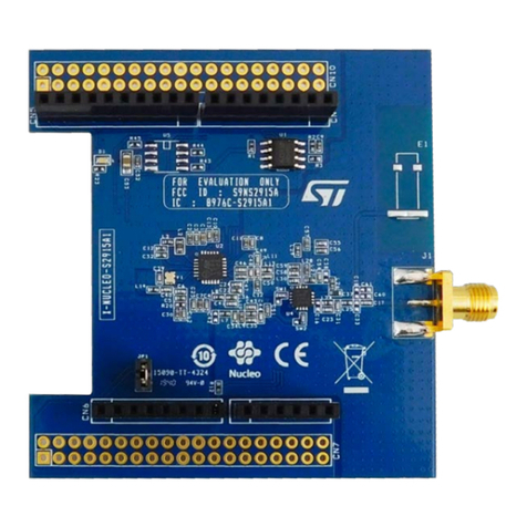
ST X-NUCLEO-OUT09A1 User manual

ST
ST ST25DV-DISCOVERY User manual

ST
ST STM32Cube User manual

ST
ST 32F412GDISCOVERY User manual

ST
ST X-NUCLEO-S915A1 User manual

ST
ST X-NUCLEO-IHM09M1 User manual

ST
ST STM32 Nucleo User manual

ST
ST X-NUCLEO-GFX01M Series User manual

ST
ST X-CUBE-CELLULAR User manual

ST
ST X-CUBE-OUT3 User manual
Popular Computer Hardware manuals by other brands

Simonds
Simonds CLP-274 Owners & safety manual

Seagate
Seagate Nytro 5350S NVMe SSD product manual

Avalue Technology
Avalue Technology ECM-TGUC user manual

PS Audio
PS Audio MultiWave II Installation and operation instructions

ekwb
ekwb EK-Quantum Vector FE RTX 3070 user guide

Cypress
Cypress CY62167DV18 Specification sheet