ST STEVAL-STWINBX1 User manual

Introduction
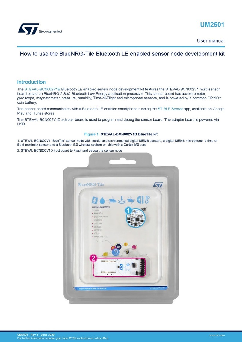
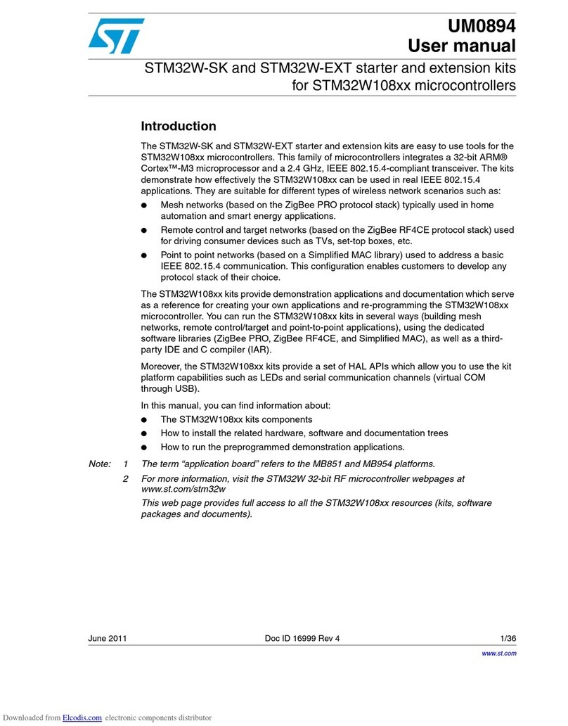
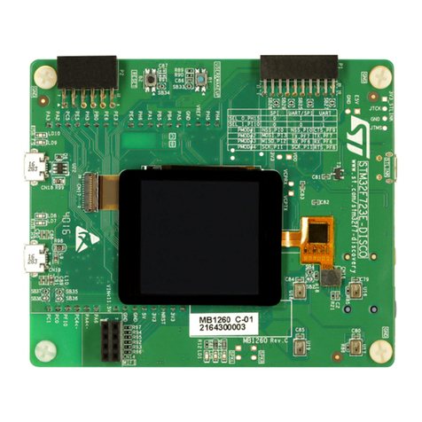
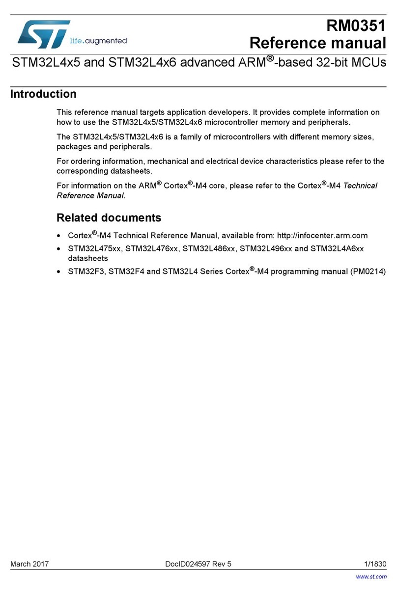
The STWIN.box (STEVAL-STWINBX1) is a development kit and reference design that simplifies prototyping and testing of
advanced industrial sensing applications in IoT contexts such as condition monitoring and predictive maintenance.
It is an evolution of the original STWIN kit (STEVAL-STWINKT1B) and features a higher mechanical accuracy in the
measurement of vibrations, an improved robustness, an updated BoM to reflect the latest and best-in-class MCU and industrial
sensors, and an easy-to-use interface for external add-ons.
The STWIN.box kit consists of an STWIN.box core system, a 480mAh LiPo battery, an adapter for the ST-LINK debugger, a
plastic case, an adapter board for DIL 24 sensors and a flexible cable.
The many on-board industrial-grade sensors and the ultra-low power MCU enable applications that feature: ultra-low power,
9 DoF motion sensing, wide-bandwidth vibration analysis, audio and ultrasound acoustic inspection, very precise local
temperature, and environmental monitoring.
A rich set of software packages is available in source code. Optimized firmware libraries and a complete companion cloud
application help to speed up the design cycle to develop end-to-end solutions.
The kit supports a broad range of connectivity options, including the built-in RS485 transceiver, BLE, Wi-Fi, and NFC.
The STWIN.box also includes a 34-pin expansion connector for small form factor daughter boards associated with the STM32
family, such as the STEVAL-C34KAT1 vibrometer and temperature sensors expansion board.
The STWIN.box is suitable for field trials, demonstrations, and PoC for industrial IoT applications that use ST software and
third-party software.
Figure 1. STWIN.box mounted with the plastic case
Getting started with the STEVAL-STWINBX1 SensorTile wireless industrial node
development kit
UM2965
User manual
UM2965 - Rev 1 - December 2022
For further information contact your local STMicroelectronics sales office. www.st.com

1Getting started
1.1 Precautions for use
Warning: Charge your device with a DC 5 V–500 mA USB charger at a temperature from 10°C to
35°C.
The kit must be used within the working temperature range. It must never be exposed to
excessive heat such as direct sunlight, fire, or heating equipment.
Danger: Use only USB chargers equipped with short-circuit protections to prevent fire hazard.
Danger: Use only the LiPo battery provided with the kit (HiMax 752535). A replacement of the battery
with an incorrect type can defeat a safeguard.
LiPo batteries can be damaged and even explode if they are short-circuited or overcharge
or with an improper usage, such as mechanical crushes, hot oven, or battery cutting.
1.2 Features
• Multisensing wireless platform for vibration monitoring and ultrasound detection
•Built around STWIN.box core system board with processing, sensing, connectivity, and expansion
capabilities
• Ultra-low power Arm® Cortex®-M33 with FPU and TrustZone at 160 MHz, 2048 kBytes Flash memory
(STM32U585AI)
• MicroSD card slot for standalone data logging applications
• On-board Bluetooth® low energy v5.0 wireless technology (BlueNRG-M2), Wi-Fi (EMW3080) and NFC
(ST25DV04K)
• Option to implement authentication and brand protection secure solution with STSAFE-A110
• Wide range of industrial IoT sensors:
– Ultra-wide bandwidth (up to 6 kHz), low-noise, 3-axis digital vibration sensor (IIS3DWB)
– 3D accelerometer + 3D gyro iNEMO inertial measurement unit (ISM330DHCX) with Machine
Learning Core
– High-performance ultra-low-power 3-axis accelerometer for industrial applications (IIS2DLPC)
– Ultra-low power 3-axis magnetometer (IIS2MDC)
– High-accuracy, high-resolution, low-power, 2-axis digital inclinometer with Embedded Machine
Learning Core (IIS2ICLX)
– Dual full-scale, 1.26 bar and 4 bar, absolute digital output barometer in full-mold package
(ILPS22QS)
– Low-voltage, ultra low-power, 0.5°C accuracy I²C/SMBus 3.0 temperature sensor (STTS22H)
– Industrial grade digital MEMS microphone (IMP34DT05)
– Analog MEMS microphone with frequency response up to 80 kHz (IMP23ABSU)
• Expandable via a 34-pin FPC connector
1.3 Kit components
The STEVAL-STWINBX1 development kit includes:
• the STWIN core system (main board);
• a plastic case with M3 bolts;
• a 480 mAh 3.7 V LiPo battery;
• STEVAL-MKIGIBV4 ST-LINK adapter with programming cable;
• an adapter board for DIL24 sensors with a flexible cable.
UM2965
Getting started
UM2965 - Rev 1 page 2/58

Figure 2. STEVAL-STWINBX1 components
1.4 Layout of the core system board (STEVAL-STWINBX1) components
Figure 3. Layout of the core system board top components
UM2965
Layout of the core system board (STEVAL-STWINBX1) components
UM2965 - Rev 1 page 3/58

Figure 4. Layout of the core system board bottom components
1.5 Core system board
Figure 5. STEVAL-STWINBX1 block diagram
UM2965
Core system board
UM2965 - Rev 1 page 4/58

Figure 6. STEVAL-STWINBX1 evaluation kit (top view)
Figure 7. STEVAL-STWINBX1 evaluation kit (bottom view)
1.6 Functional blocks
1.6.1 Sensing
The core system board offers a comprehensive range of sensors specifically designed to support industrial
applications and satisfy the demanding requirements of the Industry 4.0.
UM2965
Functional blocks
UM2965 - Rev 1 page 5/58

Figure 8. STEVAL-STWINBX1 - overview of the sensing components
The motion sensors communicate with the STM32U585AI microcontroller via SPI in order to accommodate the
high data rates, whereas the magnetometer and environmental sensors communicate via I²C. The suitably filtered
signal from the IMP23ABSU analog microphone is amplified by a TSV912 op-amp and then sampled by the
internal 12-bit ADC of the MCU. The signal from the digital microphone is directly managed by the audio digital
filter (ADF) interface of the MCU.
Figure 9. STEVAL-STWINBX1 - sensors on the top side
UM2965
Functional blocks
UM2965 - Rev 1 page 6/58

Figure 10. STEVAL-STWINBX1 - sensors on the bottom side
• U3: ILPS22QS MEMS pressure sensor
•U6: STTS22H digital temperature sensor
• U8: TSV912 wide-bandwidth (8 MHz) rail-to-rail I/O op-amp
• U9: ISM330DHCX iNEMO IMU, 3D accelerometer and 3D gyroscope with Machine Learning Core and
Finite State Machine
• U11: IIS3DWB wide bandwidth accelerometer
• U12: IIS2DLPC high-performance ultra-low-power 3-axis accelerometer for industrial applications
• U13: IIS2MDC 3-axis magnetometer
• U21: IIS2ICLX high-accuracy, high-resolution, low-power, 2-axis digital inclinometer with Machine Learning
Core
• M1: IMP23ABSU analog MEMS microphone
• M2: IMP34DT05 digital MEMS microphone
1.6.1.1 ILPS22QS
The ILPS22QS is an ultra-compact piezoresistive absolute pressure sensor, which functions as a digital output
barometer. It supports dual full-scale up to 4 bar, selectable by the user.
The ILPS22QS embeds a sensing element and an IC interface that communicates over I²C, MIPI I3CSM or SPI
interfaces from the sensing element to the application. It also supports a 1.2 V digital interface.
The ILPS22QS features an analog hub-sensing functionality, which is able to connect an analog input and convert
it to a digital signal for embedded processing.
The ILPS22QS is available in a full-mold, holed LGA package. It is guaranteed to operate over a temperature
range extending from -40°C to +105°C. The package is holed to allow the external pressure to reach the sensing
element.
Table 1. ILPS22QS I/O configuration
I/O Configuration
PH4 I2C2_SCL
PF0 I2C2_SDA
1.6.1.2 STTS22H
The STTS22H is an ultra-low-power, high-accuracy, digital temperature sensor. It offers a high performance over
the entire operating temperature range.
The STTS22H is coupled with an ASIC featuring A/D converter, signal processing logic, and an I²C/SMBus 3.0
interface.
UM2965
Functional blocks
UM2965 - Rev 1 page 7/58

The sensor is housed in a small 2 x 2 x 0.50 mm 6-lead UDFN package with the exposed pad down for a better
temperature match with the surrounding environment.
The STTS22H is factory-calibrated and requires no additional calibration.
The STTS22H units are 100% tested on a production setup that is NIST traceable and verified with equipment
calibrated in accordance with the IATF 16949:2016 standard.
Table 2. STTS22H I/O configuration
I/O Configuration
PH4 I2C2_SCL
PF0 I2C2_SDA
PF5 INT
1.6.1.3 TVS912
The TSV91x and TSV91xA operational amplifiers offer low voltage operation and rail-to-rail input and output.
They also offer an excellent speed/power consumption ratio, providing an 8 MHz gain-bandwidth product while
consuming only 1.1 mA maximum at 5 V.
The op amps are unity-gain stable and feature an ultra-low input bias current. The devices are ideal for sensor
interfaces, battery-supplied, and portable applications, as well as active filtering.
1.6.1.4 ISM330DHCX
The ISM330DHCX is a system-in-package that features a high-performance 3D digital accelerometer and a 3D
digital gyroscope tailored for Industry 4.0 applications.
The various sensing elements are manufactured using specialized micromachining processes, while the IC
interfaces are developed using CMOS technology that allows the design of a dedicated circuit, which is trimmed
to match the characteristics of the sensing element.
In the ISM330DHCX the sensing elements of the accelerometer and of the gyroscope are implemented on the
same silicon die, guaranteeing superior stability and robustness.
The ISM330DHCX has a full-scale acceleration range of ±2/±4/±8/±16 g and a wide angular rate range of
±125/±250/±500/±1000/±2000/±4000 dps that enables its usage in a broad range of applications.
All the design aspects and the calibration of the ISM330DHCX have been optimized to reach superior accuracy,
stability, extremely low noise, and full data synchronization. The embedded features (Machine Learning Core,
programmable FSM, FIFO, sensor hub, event decoding, and interrupts) enable smart and complex sensor nodes,
which deliver high performance at very low power.
The ISM330DHCX is available in a 14-lead plastic land grid array (LGA) package.
Table 3. ISM330DHCX I/O configuration
I/O Configuration
PI1 SPI2_CLK
PI3 SPI2_MOSI
PD3 SPI2_MISO
PH15 SPI_CS
PB8 INT1
PF4 INT2
1.6.1.5 IIS3DWB
The IIS3DWB is a system-in package that features a 3-axis digital vibration sensor with low noise over an
ultra-wide and flat frequency range.
The wide bandwidth, low noise, very stable, repeatable sensitivity, and the capability of operating over an
extended temperature range (up to +105°C) make the device particularly suitable for vibration monitoring in
industrial applications.
UM2965
Functional blocks
UM2965 - Rev 1 page 8/58

The high performance delivered at low power consumption, the digital output, and the embedded digital features,
such as FIFO and the interrupts, enable features for battery-operated industrial wireless sensor nodes.
The IIS3DWB has a selectable full-scale acceleration range of ±2/±4/±8/±16 g and is capable of measuring
accelerations with a bandwidth up to 6 kHz with an output data rate of 26.7 kHz.
The device integrates a 3 kB first-in, first-out (FIFO) buffer to avoid any data loss and to limit intervention of the
host processor.
The ST MEMS sensor module family leverages the robust and mature manufacturing processes already used for
the production of micromachined accelerometers and gyroscopes to serve automotive, industrial, and consumer
markets. The sensing elements are manufactured using the ST proprietary micromachining process, whereas the
embedded IC interfaces are developed using CMOS technology.
The IIS3DWB has a self-test capability, which allows checking whether the sensor is correctly working in the final
application.
The IIS3DWB is available in a 14-lead plastic land grid array (LGA) package and is guaranteed to operate over an
extended temperature range from -40°C to +105°C.
Table 4. IIS3DWB I/O configuration
I/O Configuration
PI1 SPI2_CLK
PI3 SPI2_MOSI
PD3 SPI2_MISO
PF12 SPI_CS
PF15 INT1
- INT2
1.6.1.6 IIS2DLPC
The IIS2DLPC is a three-axis linear accelerometer with digital I²C/SPI output interface.
It has full scales of ±2g/±4g/±8g/±16g selectable by the user and can measure accelerations with output data
rates from 1.6 Hz to 1600 Hz.
The IIS2DLPC has a high-performance mode and four low-power modes, which can be changed on-the-fly,
providing outstanding versatility and adaptability to the requirements of the application.
The accelerometer has an integrated 32-level first-in, first-out (FIFO) buffer that allows the user to store data in
order to limit intervention by the host processor. The embedded self-test capability allows checking whether the
sensor is correctly working in the final application.
The IIS2DLPC has a dedicated internal engine to process motion and acceleration detection, including free-fall,
wake-up, highly configurable single/double-tap recognition, activity/inactivity, stationary/motion detection, portrait/
landscape detection, and 6D/4D orientation.
The IIS2DLPC is available in a small thin plastic land grid array package (LGA) and it is guaranteed to operate
over an extended temperature range from -40°C to +85°C.
Table 5. IIS2DLPC I/O configuration
I/O Configuration
PI1 SPI2_CLK
PI3 SPI2_MOSI
PD3 SPI2_MISO
PH6 SPI_CS
PF1 INT1
PF2 INT2
UM2965
Functional blocks
UM2965 - Rev 1 page 9/58

1.6.1.7 IIS2ICLX
The IIS2ICLX is a high-accuracy (ultra-low noise, high stability, and repeatability) and low-power two-axis linear
accelerometer with digital output.
The IIS2ICLX has a selectable full scale of ±0.5/±1/±2/±3 g. It can provide the measured accelerations to the
application over an I²C or SPI digital interface. Its high accuracy, stability over temperature, and repeatability
make IIS2ICLX particularly suitable for inclination measurement applications (inclinometers).
The sensing element is manufactured using a dedicated micromachining process developed by
STMicroelectronics to produce inertial sensors and actuators on silicon wafers.
The IC interface is manufactured using a CMOS process that allows a high level of integration to design a
dedicated circuit, which is trimmed to match the characteristics of the sensing element.
The IIS2ICLX has an unmatched set of embedded features (programmable FSM, machine learning core, sensor
hub, FIFO, event decoding, and interrupts). These features are enablers for implementing smart and complex
sensor nodes, which deliver high accuracy and performance at very low power.
The IIS2ICLX is available in a high-performance (low-stress) ceramic cavity land grid array (CCLGA) package. It
can operate within a temperature range of -40°C to +105°C.
Table 6. IIS2ICLX I/O configuration
I/O Configuration
PI1 SPI2_CLK
PI3 SPI2_MOSI
PD3 SPI2_MISO
PI7 SPI_CS
PF3 INT1
PF11 INT2
1.6.1.8 IIS2MDC
The IIS2MDC is a high-accuracy, ultra-low-power, 3-axis digital magnetic sensor. It features a magnetic field
dynamic range up to ±50 gausses.
The IIS2MDC includes an I²C serial bus interface, which supports standard, fast mode, fast mode plus, and
high-speed (100 kHz, 400 kHz, 1 MHz, and 3.4 MHz), and an SPI serial standard interface.
You can configure the device to generate an interrupt signal for magnetic field detection.
The IIS2MDC is available in a plastic land grid array package (LGA) and is guaranteed to operate over an
extended temperature range from -40°C to +85°C.
Table 7. IIS2MDC I/O configuration
I/O Configuration
PH4 I2C2_SCL
PF0 I2C2_SDA
PF9 INT
1.6.1.9 IMP23ABSU
The IMP23ABSU is a compact, low-power microphone with a capacitive sensing element and an IC interface.
The sensing element, capable of detecting acoustic waves, is manufactured using a specialized silicon-
micromachining process to produce audio sensors.
The IMP23ABSU has an acoustic overload point of 130 dBSPL with a typical 64 dB signal-to-noise ratio.
The microphone sensitivity is -38 dBV ±1 dB at 94 dBSPL, 1 kHz.
The IMP23ABSU is available in a package compliant with reflow soldering and is guaranteed to operate over an
extended temperature range from -40°C to +85°C.
UM2965
Functional blocks
UM2965 - Rev 1 page 10/58

Table 8. IMP23ABSU I/O configuration
I/O Configuration
PC1 ADC1_IN2
PC0 ADC1_IN1 (REF)
1.6.1.10 IMP34DT05
The IMP34DT05 is an ultra-compact, low-power, omnidirectional, digital MEMS microphone with a capacitive
sensing element and an IC interface.
The sensing element, capable of detecting acoustic waves, is manufactured using a specialized silicon-
micromachining process dedicated to producing audio sensors.
The IC interface is manufactured using a CMOS process that allows designing a dedicated circuit able to provide
a digital signal in PDM format.
The IMP34DT05 features low distortion with a 64 dB signal-to-noise ratio and -26 dBFS ±3 dB sensitivity.
The IMP34DT05 is available in a top-port, SMD-compliant, EMI-shielded package and is guaranteed to operate
over an extended temperature range from -40°C to +85°C.
Table 9. IMP34DT05I/O configuration
I/O Configuration
PE10 ADF1_SDIO
PE9 ADF1_CCK0
1.6.2 Processing and connectivity
The STWIN.box core system board features several wired and wireless connectivity options and the
STM32U585AI ultra-low-power microcontroller.
The microcontroller belongs to the STM32U5 series of ultra-low-power MCUs based on the high-performance
Arm® Cortex®-M33 with TrustZone, which operates at up to 160 MHz and embeds 786 kbytes of SRAM and 2 MB
of dual bank Flash memory.
UM2965
Functional blocks
UM2965 - Rev 1 page 11/58

Figure 11. Main connectivity components and the STM32U585AI processing unit
Each connectivity component is connected to an independent bus on the STM32U585AI MCU, so all of them can
be individually configured.
Figure 12. MCU and connectivity components (top view)
UM2965
Functional blocks
UM2965 - Rev 1 page 12/58

Figure 13. MCU and connectivity components (bottom view)
• U20: STM32U585AI ultra-low-power Arm® Cortex®-M33 with FPU and TrustZone at 160 MHz;
• U5: BlueNRG-M2SA Bluetooth® low energy v5.2 wireless technology module;
• U7: STSAFE-A110 authentication and brand protection secure solution;
• U18: STR485 3.3 V RS485 up to 20 mbps;
• U23: MXCHIP EMW3080 (802.11 b/g/n compliant Wi-Fi module);
• U24: ST25DV04K dynamic NFC/RFID tag IC with 64-Kbit EEPROM;
• USB: USB Type-C™ connector (power supply and data);
• CN4: STDC14 programming connector for STLINK-V3MINI;
• SDCard: microSD card socket.
1.6.2.1 STM32U585AI
The STM32U585xx device belongs to an ultra-low-power microcontrollers family (STM32U5 series) based on the
high-performance Arm® Cortex®-M33 32-bit RISC core. They operate at a frequency of up to 160 MHz.
The Arm® Cortex®-M33 core features a single-precision FPU (floating-point unit), which supports all the Arm®
single-precision data-processing instructions and all the data types. It also implements a full set of digital signal
processing (DSP) instructions and a memory protection unit (MPU) that enhances the application security.
The device embeds high-speed memories (2 mbytes of Flash memory and 786 kbytes of SRAM), a flexible
external memory controller (FSMC) for static memories (for devices with packages of 90 pins and more), two
octo-SPI Flash memory interfaces (at least one quad-SPI available on all packages), an extensive range of
enhanced I/Os and peripherals connected to three APB buses, three AHB buses, and a 32-bit multi-AHB bus
matrix.
The device offers security foundation compliant with the trusted-based security architecture (TBSA) requirements
from Arm®. It embeds the necessary features to implement a secure boot, secure data storage, and secure
firmware update.
The device also incorporates a secure firmware installation feature that allows the customer to secure the
provisioning of the code during its production.
A flexible lifecycle is managed thanks to multiple levels of readout protection and debug unlock with password.
Firmware hardware isolation is supported thanks to securable peripherals, memories and I/Os, and privilege
configuration of peripherals and memories.
The device features several protection mechanisms for embedded Flash memory and SRAM: readout protection,
write protection, secure, and hide protection areas. They also embed several peripherals reinforcing security: a
fast AES coprocessor, a secure AES coprocessor with DPA resistance, and a hardware unique key that can be
shared by hardware with fast AES, a public key accelerator (PKA) with DPA resistance, an on-the-fly decryption
engine for octo-SPI external memories, a HASH hardware accelerator, and a true random number generator.
The device also features active tamper detection and protection against transient and environmental perturbation
attacks, thanks to several internal monitoring generating secret data erase in case of attack. This helps to fit the
PCI requirements for point of sales applications.
UM2965
Functional blocks
UM2965 - Rev 1 page 13/58

The device offers one fast 14-bit ADC (2.5 Msps), one 12-bit ADC (2.5 Msps), two comparators, two operational
amplifiers, two DAC channels, an internal voltage reference buffer, a low-power RTC, four 32-bit general-purpose
timers, two 16-bit PWM timers dedicated to motor control, three 16-bit general-purpose timers, two 16-bit basic
timers, and four 16-bit low-power timers. The device supports a multifunction digital filter (MDF) with six filters
dedicated to the connection of external sigma-delta modulators. Another low-power digital filter dedicated to audio
signals is embedded (ADF), with one filter supporting sound-activity detection.
The device embeds a Chrom-ART accelerator dedicated to graphic applications, and mathematical accelerators
(a trigonometric functions accelerator plus a filter mathematical accelerator). In addition, up to 24 capacitive
sensing channels are available.
The device also features standard and advanced communication interfaces such as: four I2Cs, three SPIs,
three USARTs, two UARTs, one low-power UART, two SAIs, one digital camera interface (DCMI), two SDMMCs,
one FDCAN, one USB OTG full-speed, one USB Type-C /USB Power Delivery controller, and one generic
synchronous 8-/16-bit PSSI (parallel data input/output slave interface). The device operates in the -40 to +85°C
(+105°C junction) and -40 to +125°C (+130°C junction) temperature ranges from a 1.71 to 3.6 V power supply.
A comprehensive set of power-saving modes allows the design of low-power applications. Many peripherals
(including communication, analog, timers, and audio peripherals) can be functional and autonomous down to stop
mode with direct memory access, thanks to low-power background autonomous mode (LPBAM).
Some independent power supplies are supported like an analog independent supply input for ADC, DACs,
OPAMPs and comparators, a 3.3 V dedicated supply input for USB and up to 14 I/Os, that can be supplied
independently down to 1.08 V. A VBAT input is available for connecting a backup battery in order to preserve the
RTC functionality and to back up 3232-bit registers and 2-Kbyte SRAM. The devices offer eight packages from 48
to 169 pins.
1.6.2.2 BlueNRG-M2
The BlueNRG-M2 is a Bluetooth® Low Energy system-on-chip application processor certified module, compliant
with BT specifications v5.2 and BQE qualified.
The module supports multiple roles simultaneously and can act at the same time as a Bluetooth® Low Energy
master and a slave device.
It is based on the BlueNRG-2 system-on-chip and embeds the entire Bluetooth® Low Energy stack and protocols.
The BlueNRG-2 module provides a complete RF platform in a tiny form factor. The integrated radio, the
embedded antenna, and the high frequency oscillators offer a certified solution to optimize the time-to-market
of the final applications.
• Operating band: 2402 MHz to 2480 MHz
• Channel spacing: 2 MHz
• RF power: +5 dBm
Table 10. BlueNRG2-M2 I/O configuration
I/O Configuration
PG9 SPI3_CLK
PB5 SPI3_MOSI
PB4 SPI3_MISO
PE1 SPI_CS
PF14 INT
PD13 RESET
1.6.2.3 MXCHIP EMW3080
The MXCHIP EMW3080 module is an embedded device for Internet wireless connectivity. The module uses the
SPI2 interface of the STM32U585AI to communicate with the MCU.
This Wi-Fi module requires no operating system and has a completely integrated TCP/IP stack that requires only
AT commands to establish the connection.
UM2965
Functional blocks
UM2965 - Rev 1 page 14/58

Figure 14. MXCHIP EMW3080
The main features of the MXCHIP EMW3080 module are:
•IEEE 802.11n D7.0, OFDM-72.2 Mbps, single-stream width of 20 MHz, and short GI;
• IEEE 802.11g, OFDM 54 Mbps;
• IEEE 802.11b, DSSS 11 Mbps;
• IEEE 802.11i, security–Wi-Fi protected access (WPA)–PSK/TKIP–Wi-Fi protected access 2 (WPA2)–AES/
CCMP/802.1x authentication;
• GPIO, five ADCs (the SPI interface uses the ADC pins);
• Operating band: 2400 MHz ~ 2483.5 MHz (2.4 GHz ISM band)
• RF power: 16 dBm
• Power-saving mode allows the design of low-power applications;
• Lead-free design compliant with RoHS requirements;
• EMI/EMC metal shield to achieve the best RF performance in noisy environments and to accommodate for
lower RF emissions/signature for easier FCC compliance;
• FCC/CE compliance certification.
Table 11. MXCHIP EMW3080 I/O configuration
I/O Configuration
PG2 SPI1_CLK
PG4 SPI1_MOSI
PG3 SPI1_MISO
PH7 SPI_CS
PG15 INT (Flow)
PE7 INT (Notify)
PE12 Chip_En
1.6.2.4 STR485
The STR485 is a low-power differential line transceiver for data transmission standard RS485 applications in
half-duplex mode.
Data and enable signals are compatible with 1.8 V or 3.3 V supplies.
Two speeds are selectable through the SLR pin: fast data rate up to 20 Mbps or slow data rate for extended cable
running to 250 kbps.
The thermal shutdown circuit prevents excessive power dissipation due to bus contention or faults. This circuit
forces the driver outputs into a high impedance state.
The receiver has a fail-safe feature, which guarantees a high output state when the inputs are left open, shorted,
or idle.
UM2965
Functional blocks
UM2965 - Rev 1 page 15/58

Table 12. STR485LV I/O configuration
I/O Configuration
PA7 USART3_TX
PA5 USART3_RX
PD12 USART3_RTS
1.6.2.5 USB connector
The on-board USB Type-C connector can be used for both power supply and data transfer (USB device only).
You can find several examples of USB class implementation in the STM32 software packages.
Table 13. USB connector I/O configuration
I/O Configuration
PA12 USB_OTG_DP
PA11 USB_OTG_DM
1.6.2.6 STSAFE-A110
The STSAFE-A110 is a highly secure element that provides authentication and secure data management services
to a local or remote host. It consists of a full turnkey solution with a secure operating system, which runs on the
latest generation of secure microcontrollers.
The STSAFE-A110 can be integrated in IoT devices, smart-home, smart-city, industrial applications, consumer
electronics devices, consumables, and accessories.
Table 14. STSAFE-A110 I/O configuration
I/O Configuration
PB6 I2C1_SCL
PB9 I2C1_SDA
PH9 RESET
1.6.2.7 MicroSD card socket
On the bottom side of the STWIN.box core system board is a microSD card socket that is accessible even when
the board is mounted in the plastic case.
A four-bit wide SDIO port allows accessing the card for the maximum performance.
Table 15. Micro-SD card socket I/O configuration
I/O Configuration
PC8 SDMMC_D0
PC9 SDMMC_D1
PC10 SDMMC_D2
PC11 SDMMC_D3
PC12 SDMMC_CK
PD2 SDMMC_CMD
PG1 SD_Detect
1.6.2.8 Clock sources
There are two external clock sources on the STWIN.box core system board:
UM2965
Functional blocks
UM2965 - Rev 1 page 16/58

• X1, which is a 16 MHz high speed external (HSE) oscillator for the MCU;
•X2, which is a 32.768 kHz low speed external (LSE) oscillator for the RTC embedded in the MCU.
1.6.3 Power management
The STWIN.box core system board includes a wide range of power management features that enable very low
power consumption in final applications.
The main supply is a lithium ion polymer battery (3.7 V, 480 mAh) and the integrated battery charger (STBC02)
with VIN from 4.8 to 5.5 V.
The STWIN core system board includes a range of power management features that enable very low power
consumption in final applications. The main supply is through a lithium ion polymer battery (3.7 V, 480 mAh) and
the integrated battery charger (STBC02) with Vin [4.8 -5.5 V].
Figure 15. Power management of the STWIN.box core system board
Figure 16. Power and protections
Power management IC
•U1: EMIF06-MSD02N16 six-line IPAD, EMI filter and ESD protection
• U10: LDLN025PU275R, 250 mA ultra low noise LDO
UM2965
Functional blocks
UM2965 - Rev 1 page 17/58

• U16, U19: ST1PS02CQ, 400 mA synchronous step-down converter
•U15: STBC02AJR Li-Ion linear battery charger
• U22: TCPP01-M12, USB Type-C™ port protection for Sink applications
• U25: STEF05SGR, electronic fuse for 5 V line
• Q1: STL6N3LLH6, N-channel 30 V, 6 A power MOSFET
Protections and connectors
• U17: USBLC6-2P6, low capacitance ESD protection for USB
• D4: STPS120M, 20 V, 1 A STmite power Schottky rectifier
• D6: ESDA25P35-1U1M, high-power transient voltage suppressor (TVS)
• TVS1, TVS2, TVS3: ESDALC6V1-1M2, single line low capacitance Transil
• TVS4: USBULC6-2M6, ultra large bandwidth ESD protection
• BATT, J4: battery connector
• J5: 5 V external power supply connector
• PWR: power button
1.6.3.1 TCPP01-M12
The TCPP01-M12 USB Type-C™ port protection is a single chip that facilitates the migration from USB legacy
connectors Type-A or Type-B to USB Type-C™ connectors.
The TCPP01-M12 features a 22 V tolerant ESD protection as per IEC61000-4-2 level 4 on the USB Type-C™
connector configuration channel (CC) pins.
For a safe and reliable USB Type-C™ implementation, the TCPP01-M12 provides overvoltage protection on
CC1 and CC2 pins when these pins are subjected to short-circuit with the VBUS pin. This might happen when
removing the USB Type-C™ cable from its receptacle.
For sink applications, the TCPP01-M12 triggers an external N-MOSFET on the VBUS line when a defective
power source applies a voltage higher than the selected OVP threshold. Moreover, the TCPP01-M12 integrates a
dead-battery management logic that is compliant with the latest USB power delivery specification.
The TCPP01-M12 power supply for sink applications operated with a battery can be provided by an MCU 3.3 V
GPIO to drop the power consumption in the "cable not attached” condition down to 0 nA. This low-power mode
extends the battery operating life when no source equipment is attached.
The TCPP01-M12 can also be used to protect source (provider) applications. It can support the programmable
power supply feature from the USB Type-C™ power delivery specification.
1.6.3.2 STEF05S
The STEF05S is an integrated electronic fuse optimized to monitor the 5 V DC power lines. When connected in
series to the main power rail, it is able to detect precisely and react to overcurrent and overvoltage conditions.
When an overload condition occurs, the device limits the output current to a user-defined safe value. If the
overload condition persists, the device enters an open state by disconnecting the load from the power supply.
In the case of an input overvoltage, the device regulates the output to a preset safe value.
The undervoltage lockout prevents the load from malfunctioning, switching the device off if the rail voltage is too
low.
The STEF05S features the adjustable turn-on slew rate, which is useful to keep the inrush current under control
during startup and hot-swap operations.
1.6.3.3 EMIF06-MSD02N16
The EMIF06-MSD02N16 is a six-line, highly integrated device designed to suppress EMI/RFI noise in all systems
exposed to electromagnetic interference. This filter includes an ESD protection circuitry, which prevents damage
to the application when subjected to ESD surges.
1.6.3.4 LDLN025
The LDLN025 is a 250 mA low-dropout voltage regulator, which works with an input voltage range from 1.5 to 5.5
V.
The typical dropout voltage at 250 mA load is 120 mV. The very low quiescent current, which is just 12 μA at
no-load, extends the battery life of applications that require a very long standby time.
UM2965
Functional blocks
UM2965 - Rev 1 page 18/58

Thanks to its ultra-low noise value and high PSRR, the LDLN025 provides a very clean output, suitable for
ultra-sensitive loads. It is stable with ceramic capacitors.
The enable logic control function makes the device enter shutdown mode, with a total current consumption lower
than 1 μA.
The device also includes short-circuit and thermal protections.
Typical applications are noise-sensitive loads such as ADC, VCO in mobile phones and tablets, and wireless LAN
devices.
The LDLN025 is designed to keep the quiescent current under control, at a low value also during the dropout
operation.
1.6.3.5 ST1PS02
The ST1PS02 is a nano-quiescent miniaturized synchronous step-down converter, which is able to provide up to
400 mA output current with an input voltage ranging from 1.8 to 5.5 V.
This converter is designed for applications where the key factors are high efficiency, PCB size, and thickness.
The output voltage can be set using three digital control inputs. A VOUT from 1.0 to 3.3 V can be dynamically
selected.
Thanks to the enhanced peak current control (PCC), the ST1PS02 reaches a very high efficiency conversion
using just a 2.2 µH inductor and two small capacitors.
The device embeds a controlled load switch to supply a subsystem with the same voltage rail. The advanced
design circuitry is implemented to minimize the quiescent current. The device is available in a thin plastic
package.
1.6.3.6 STBC02
The STBC02 is a highly integrated power management device. It embeds a linear battery charger, a 150 mA
LDO, two SPDT load switches, a smart reset/watchdog block, and a protection circuit module (PCM) to prevent
battery damage under fault conditions.
The STBC02 uses a CC/CV algorithm to charge the battery. You can program the fast charge and the precharge
current independently by using dedicated resistors.
The termination current is set by default, being 5% of the programmed fast charge current, but you can also fix it
at different values. Likewise, you can program the battery-floating voltage value and set it to a value up to 4.45 V.
The STBC02 also features a charger enable input to stop the charging process anytime.
The STBC02 is automatically powered off from the connected battery when the IN pin is not connected
to a valid power source (battery mode). An external circuitry (NTC thermistor) can detect any battery under/
overtemperature condition.
The STBC02 draws less than 10 nA from the connected battery in shipping mode conditions in order to maximize
the battery life. The device is available in a flip-chip package.
1.6.3.7 USBLC6-2
The USBLC6-2SC6 is a device specific for monolithic applications dedicated to ESD protection of high-speed
interfaces, such as USB 2.0, Ethernet links, and video lines.
The very low line capacitance secures a high level of signal integrity without compromising sensitive chip
protection against the most stringently characterized ESD strikes.
1.6.3.8 Battery connectors
Connect the 480 mA LiPo battery included in the STWIN.box kit to the dedicated battery connector (BATT1) in
order to provide the battery supply voltage (VBAT).
UM2965
Functional blocks
UM2965 - Rev 1 page 19/58

Figure 17. BATT1 connector
Table 16. BATT1 connector pins and signals
Signal BATT1 connector
GND Pin 1
BAT_NC Pin 2
VBAT Pin 3
1.6.3.9 Power supply
Different sources can supply the STWIN.box core system board:
•V_USB: through USB-Type C connector (sink only, 5 V).
• VIN: through J5 connector (4.8-5.5 V).
Note: Limit the current on this port to 2 A.
• VBAT: lithium ion polymer battery (3.7 V, 480 mAh) and the STBC02 battery charger integrated in the
board.
The battery is optional. The STBC02 battery charger automatically checks the available power inputs and selects
one of them to power the system. When the battery or another source is connected, the STBC02 automatically
charges the battery.
When battery-powered, the equipment is intended to work properly with an operating temperature of 35°C.
Without the battery, the equipment is intended to work properly with an operating temperature of 45°C.
UM2965
Functional blocks
UM2965 - Rev 1 page 20/58
Table of contents
Other ST Microcontroller manuals

ST
ST STM32H7B3I-DK User manual

ST
ST STM32F2 Series User manual

ST
ST STM32H7 3 Series Installation and operating instructions

ST
ST STM32F446 Series User manual

ST
ST STR71xF User manual

ST
ST STM32H745I-DISCO User manual

ST
ST ST624 B-EMU2 Series User manual

ST
ST STM32F7308-DK User manual

ST
ST STM32F423 Series User manual

ST
ST STM32L4 5 Series User manual
Popular Microcontroller manuals by other brands
Infineon
Infineon CY8CKIT-062-WIFI-BT quick start guide

Motorola
Motorola M68MPBF333 user manual

Espressif
Espressif ESP32--S3 Series Hardware Design Guidelines

NXP Semiconductors
NXP Semiconductors LPC824M201JHI33 user manual

Embedded Artists
Embedded Artists LPC3152 user guide

Sutter Instrument
Sutter Instrument TRIO MPC-165 Series Operation manual