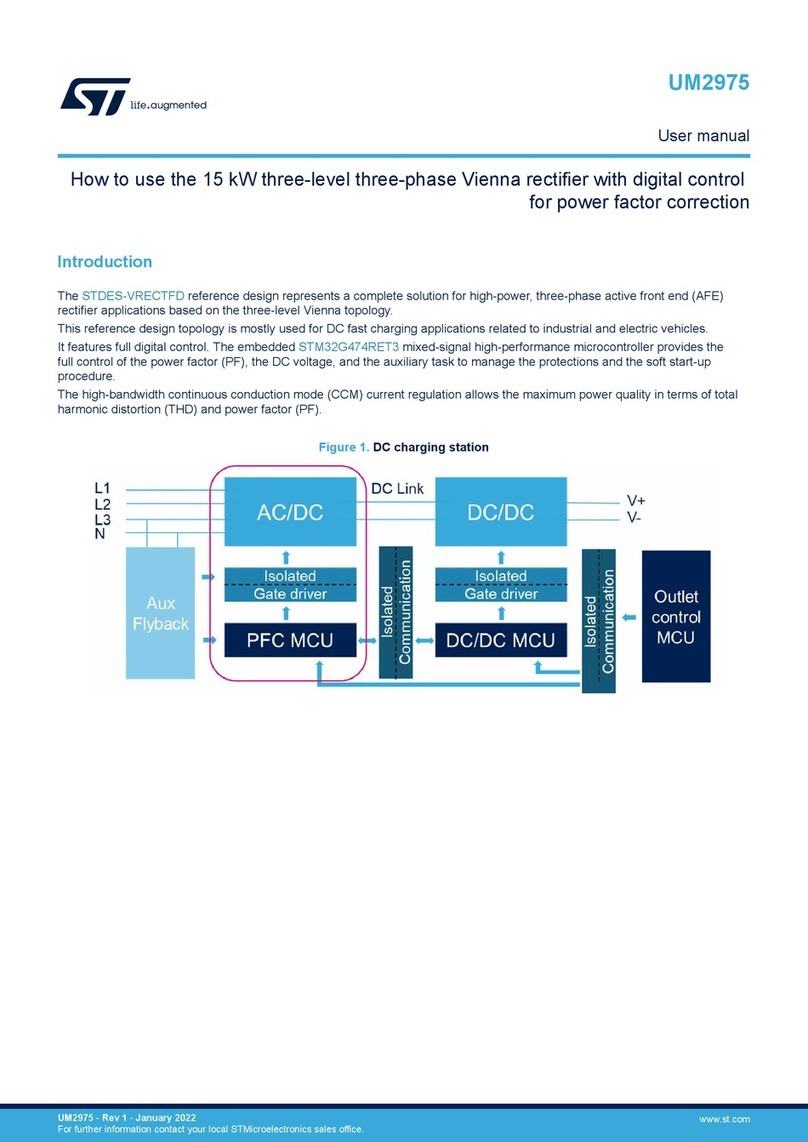
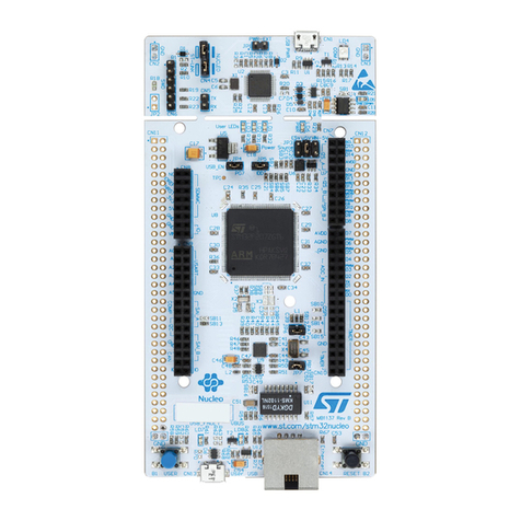
ST STM32F74 Series User manual

June 2015 DocID027559 Rev 2 1/45
1
AN4661
Application note
Getting started with STM32F74xxx/STM32F75xxx MCU hardware
development
Introduction
This application note is intended for system designers who require an hardware
implementation overview of the development board, with focus on features:
•Power supply,
•Package selection,
•Clock management,
•Reset control,
•Boot mode settings,
•Debug management.
This document describes the minimum hardware resources required to develop an
application based on the STM32F74xxx/STM32F75xxx devices.
Table 1. Applicable products
Type Part number
Microcontrollers
STM32F745IE, STM32F745VE, STM32F745IG, STM32F745VG,
STM32F745ZE, STM32F745ZG
STM32F746VG, STM32F746ZG, STM32F746IG, STM32F746BG,
STM32F746NG, STM32F746IE, STM32F746VE, STM32F746ZE,
STM32F746BE, STM32F746NE
STM32F756VG, STM32F756ZG, STM32F756IG, STM32F756BG,
STM32F756NG
www.st.com

Contents AN4661
2/45 DocID027559 Rev 2
Contents
1 Power supplies . . . . . . . . . . . . . . . . . . . . . . . . . . . . . . . . . . . . . . . . . . . . . 7
1.1 Introduction . . . . . . . . . . . . . . . . . . . . . . . . . . . . . . . . . . . . . . . . . . . . . . . . 7
1.1.1 Independent A/D converter supply and reference voltage . . . . . . . . . . . . 7
1.1.2 Independent USB transceivers supply . . . . . . . . . . . . . . . . . . . . . . . . . . . 7
1.1.3 Battery backup domain . . . . . . . . . . . . . . . . . . . . . . . . . . . . . . . . . . . . . . 8
1.1.4 Voltage regulator . . . . . . . . . . . . . . . . . . . . . . . . . . . . . . . . . . . . . . . . . . . 9
1.2 Power supply scheme . . . . . . . . . . . . . . . . . . . . . . . . . . . . . . . . . . . . . . . . 9
1.3 Reset & power supply supervisor . . . . . . . . . . . . . . . . . . . . . . . . . . . . . . . .11
1.3.1 Power-on reset (POR)/power-down reset (PDR) . . . . . . . . . . . . . . . . . . 11
1.3.2 Programmable voltage detector (PVD) . . . . . . . . . . . . . . . . . . . . . . . . . 11
1.3.3 System reset . . . . . . . . . . . . . . . . . . . . . . . . . . . . . . . . . . . . . . . . . . . . . 12
1.3.4 Internal reset ON . . . . . . . . . . . . . . . . . . . . . . . . . . . . . . . . . . . . . . . . . . 13
1.3.5 Internal reset OFF . . . . . . . . . . . . . . . . . . . . . . . . . . . . . . . . . . . . . . . . . 13
1.3.6 Regulator OFF mode . . . . . . . . . . . . . . . . . . . . . . . . . . . . . . . . . . . . . . . 14
1.3.7 Regulator ON/OFF and internal reset ON/OFF availability . . . . . . . . . . 16
2 Alternate function mapping to pins . . . . . . . . . . . . . . . . . . . . . . . . . . . . 17
3 Clocks . . . . . . . . . . . . . . . . . . . . . . . . . . . . . . . . . . . . . . . . . . . . . . . . . . . . 18
3.1 HSE OSC clock . . . . . . . . . . . . . . . . . . . . . . . . . . . . . . . . . . . . . . . . . . . . 18
3.1.1 External user clock (HSE bypass) . . . . . . . . . . . . . . . . . . . . . . . . . . . . . 18
3.1.2 External crystal/ceramic resonator (HSE crystal) . . . . . . . . . . . . . . . . . 19
3.2 LSE OSC clock . . . . . . . . . . . . . . . . . . . . . . . . . . . . . . . . . . . . . . . . . . . . . 19
3.2.1 External clock (LSE bypass) . . . . . . . . . . . . . . . . . . . . . . . . . . . . . . . . . 20
3.2.2 External crystal/ceramic resonator (LSE crystal) . . . . . . . . . . . . . . . . . . 20
3.3 Clock security system (CSS) . . . . . . . . . . . . . . . . . . . . . . . . . . . . . . . . . . 20
4 Boot configuration . . . . . . . . . . . . . . . . . . . . . . . . . . . . . . . . . . . . . . . . . 21
4.1 Boot mode selection . . . . . . . . . . . . . . . . . . . . . . . . . . . . . . . . . . . . . . . . . 21
4.2 Boot pin connection . . . . . . . . . . . . . . . . . . . . . . . . . . . . . . . . . . . . . . . . . 22
4.3 System bootloader mode . . . . . . . . . . . . . . . . . . . . . . . . . . . . . . . . . . . . . 22
5 Debug management . . . . . . . . . . . . . . . . . . . . . . . . . . . . . . . . . . . . . . . . 23
5.1 Introduction . . . . . . . . . . . . . . . . . . . . . . . . . . . . . . . . . . . . . . . . . . . . . . . 23

DocID027559 Rev 2 3/45
AN4661 Contents
4
5.2 SWJ debug port (serial wire and JTAG) . . . . . . . . . . . . . . . . . . . . . . . . . . 23
5.3 Pinout and debug port pins . . . . . . . . . . . . . . . . . . . . . . . . . . . . . . . . . . . 23
5.3.1 SWJ debug port pins . . . . . . . . . . . . . . . . . . . . . . . . . . . . . . . . . . . . . . . 24
5.3.2 Flexible SWJ-DP pin assignment . . . . . . . . . . . . . . . . . . . . . . . . . . . . . 24
5.3.3 Internal pull-up and pull-down on JTAG pins . . . . . . . . . . . . . . . . . . . . . 25
5.3.4 SWJ debug port connection with standard JTAG connector . . . . . . . . . 25
6 Recommendations . . . . . . . . . . . . . . . . . . . . . . . . . . . . . . . . . . . . . . . . . 26
6.1 Printed circuit board . . . . . . . . . . . . . . . . . . . . . . . . . . . . . . . . . . . . . . . . . 26
6.2 Component position . . . . . . . . . . . . . . . . . . . . . . . . . . . . . . . . . . . . . . . . . 26
6.3 Ground and power supply (VSS,VDD) . . . . . . . . . . . . . . . . . . . . . . . . . . . 26
6.4 Decoupling . . . . . . . . . . . . . . . . . . . . . . . . . . . . . . . . . . . . . . . . . . . . . . . . 26
6.5 Other signals . . . . . . . . . . . . . . . . . . . . . . . . . . . . . . . . . . . . . . . . . . . . . . 27
6.6 Unused I/Os and features . . . . . . . . . . . . . . . . . . . . . . . . . . . . . . . . . . . . 27
7 Reference design . . . . . . . . . . . . . . . . . . . . . . . . . . . . . . . . . . . . . . . . . . 28
7.1 Description . . . . . . . . . . . . . . . . . . . . . . . . . . . . . . . . . . . . . . . . . . . . . . . 28
7.1.1 Clocks . . . . . . . . . . . . . . . . . . . . . . . . . . . . . . . . . . . . . . . . . . . . . . . . . . 28
7.1.2 Reset . . . . . . . . . . . . . . . . . . . . . . . . . . . . . . . . . . . . . . . . . . . . . . . . . . . 28
7.1.3 Boot mode . . . . . . . . . . . . . . . . . . . . . . . . . . . . . . . . . . . . . . . . . . . . . . . 28
7.1.4 SWJ interface . . . . . . . . . . . . . . . . . . . . . . . . . . . . . . . . . . . . . . . . . . . . 28
7.1.5 Power supply . . . . . . . . . . . . . . . . . . . . . . . . . . . . . . . . . . . . . . . . . . . . . 28
7.2 Component references . . . . . . . . . . . . . . . . . . . . . . . . . . . . . . . . . . . . . . . 29
8 Recommended PCB routing guidelines for
STM32F745xx/STM32F756xx devices . . . . . . . . . . . . . . . . . . . . . . . . . . 34
8.1 PCB stack-up . . . . . . . . . . . . . . . . . . . . . . . . . . . . . . . . . . . . . . . . . . . . . . 34
8.2 Crystal oscillator . . . . . . . . . . . . . . . . . . . . . . . . . . . . . . . . . . . . . . . . . . . . 35
8.3 Power supply decoupling . . . . . . . . . . . . . . . . . . . . . . . . . . . . . . . . . . . . . 35
8.4 High speed signal layout . . . . . . . . . . . . . . . . . . . . . . . . . . . . . . . . . . . . . 36
8.4.1 SDMMC bus interface . . . . . . . . . . . . . . . . . . . . . . . . . . . . . . . . . . . . . . 36
8.4.2 Flexible memory controller (FMC) interface . . . . . . . . . . . . . . . . . . . . . . 37
8.4.3 Quadrature serial parallel interface (Quad SPI) . . . . . . . . . . . . . . . . . . . 38
8.4.4 Embedded trace macrocell (ETM) . . . . . . . . . . . . . . . . . . . . . . . . . . . . . 39
8.5 Package layout recommendation . . . . . . . . . . . . . . . . . . . . . . . . . . . . . . . 39
8.5.1 BGA 216 0.8 mm pitch design example . . . . . . . . . . . . . . . . . . . . . . . . 39

Contents AN4661
4/45 DocID027559 Rev 2
8.5.2 WLCSP143 0.4 mm pitch design example . . . . . . . . . . . . . . . . . . . . . . 41
9 Conclusion . . . . . . . . . . . . . . . . . . . . . . . . . . . . . . . . . . . . . . . . . . . . . . . . 43
10 Revision history . . . . . . . . . . . . . . . . . . . . . . . . . . . . . . . . . . . . . . . . . . . 44

DocID027559 Rev 2 5/45
AN4661 List of tables
5
List of tables
Table 1. Applicable products . . . . . . . . . . . . . . . . . . . . . . . . . . . . . . . . . . . . . . . . . . . . . . . . . . . . . . . 1
Table 2. Regulator ON/OFF and internal reset ON/OFF availability. . . . . . . . . . . . . . . . . . . . . . . . . 16
Table 3. Boot modes. . . . . . . . . . . . . . . . . . . . . . . . . . . . . . . . . . . . . . . . . . . . . . . . . . . . . . . . . . . . . 21
Table 4. STM32F74xxx/STM32F75xxx bootloader communication peripherals. . . . . . . . . . . . . . . . 22
Table 5. SWJ debug port pins . . . . . . . . . . . . . . . . . . . . . . . . . . . . . . . . . . . . . . . . . . . . . . . . . . . . . 24
Table 6. Flexible SWJ-DP assignment . . . . . . . . . . . . . . . . . . . . . . . . . . . . . . . . . . . . . . . . . . . . . . . 24
Table 7. Mandatory components . . . . . . . . . . . . . . . . . . . . . . . . . . . . . . . . . . . . . . . . . . . . . . . . . . . 29
Table 8. Optional components . . . . . . . . . . . . . . . . . . . . . . . . . . . . . . . . . . . . . . . . . . . . . . . . . . . . . 29
Table 9. Reference connection for all packages. . . . . . . . . . . . . . . . . . . . . . . . . . . . . . . . . . . . . . . . 31
Table 10. BGA 216 0.8 mm pitch package information . . . . . . . . . . . . . . . . . . . . . . . . . . . . . . . . . . . 39
Table 11. Wafer level chip scale package information . . . . . . . . . . . . . . . . . . . . . . . . . . . . . . . . . . . . 41
Table 12. Document revision history . . . . . . . . . . . . . . . . . . . . . . . . . . . . . . . . . . . . . . . . . . . . . . . . . 44

List of figures AN4661
6/45 DocID027559 Rev 2
List of figures
Figure 1. VDDUSB connected to VDD power supply . . . . . . . . . . . . . . . . . . . . . . . . . . . . . . . . . . . . . 8
Figure 2. VDDUSB connected to external power supply. . . . . . . . . . . . . . . . . . . . . . . . . . . . . . . . . . . 8
Figure 3. Power supply scheme. . . . . . . . . . . . . . . . . . . . . . . . . . . . . . . . . . . . . . . . . . . . . . . . . . . . . 10
Figure 4. Power on reset/power down reset waveform . . . . . . . . . . . . . . . . . . . . . . . . . . . . . . . . . . . 11
Figure 5. PVD threshold. . . . . . . . . . . . . . . . . . . . . . . . . . . . . . . . . . . . . . . . . . . . . . . . . . . . . . . . . . . 12
Figure 6. Reset circuit . . . . . . . . . . . . . . . . . . . . . . . . . . . . . . . . . . . . . . . . . . . . . . . . . . . . . . . . . . . . 13
Figure 7. Power supply supervisor interconnection with internal reset OFF . . . . . . . . . . . . . . . . . . . 13
Figure 8. NRST circuitry timing example for STM32F74xxx/STM32F75xxx . . . . . . . . . . . . . . . . . . . 14
Figure 9. BYPASS_REG supervisor reset connection. . . . . . . . . . . . . . . . . . . . . . . . . . . . . . . . . . . . 15
Figure 10. STM32CubeMX example screen-shot . . . . . . . . . . . . . . . . . . . . . . . . . . . . . . . . . . . . . . . . 17
Figure 11. HSE external clock . . . . . . . . . . . . . . . . . . . . . . . . . . . . . . . . . . . . . . . . . . . . . . . . . . . . . . . 18
Figure 12. HSE crystal/ceramic resonators . . . . . . . . . . . . . . . . . . . . . . . . . . . . . . . . . . . . . . . . . . . . . 18
Figure 13. LSE external clock . . . . . . . . . . . . . . . . . . . . . . . . . . . . . . . . . . . . . . . . . . . . . . . . . . . . . . . 19
Figure 14. LSE crystal/ceramic resonators . . . . . . . . . . . . . . . . . . . . . . . . . . . . . . . . . . . . . . . . . . . . . 19
Figure 15. Boot mode selection implementation example . . . . . . . . . . . . . . . . . . . . . . . . . . . . . . . . . . 22
Figure 16. Host to board connection . . . . . . . . . . . . . . . . . . . . . . . . . . . . . . . . . . . . . . . . . . . . . . . . . . 23
Figure 17. JTAG connector implementation . . . . . . . . . . . . . . . . . . . . . . . . . . . . . . . . . . . . . . . . . . . . 25
Figure 18. Typical layout for VDD/VSS pair. . . . . . . . . . . . . . . . . . . . . . . . . . . . . . . . . . . . . . . . . . . . . 27
Figure 19. STM32F756NGH6 reference schematic . . . . . . . . . . . . . . . . . . . . . . . . . . . . . . . . . . . . . . 30
Figure 20. Four layer PCB stack-up example . . . . . . . . . . . . . . . . . . . . . . . . . . . . . . . . . . . . . . . . . . . 34
Figure 21. Six layer PCB stack-up example . . . . . . . . . . . . . . . . . . . . . . . . . . . . . . . . . . . . . . . . . . . . 35
Figure 22. Example of bypass cap placed underneath the STM32F74xxx/STM32F75xxx . . . . . . . . . 36
Figure 23. BGA 0.8mm pitch example of fan-out. . . . . . . . . . . . . . . . . . . . . . . . . . . . . . . . . . . . . . . . . 40
Figure 24. Via fan-out . . . . . . . . . . . . . . . . . . . . . . . . . . . . . . . . . . . . . . . . . . . . . . . . . . . . . . . . . . . . . 40
Figure 25. FMC signal fan-out routing example. . . . . . . . . . . . . . . . . . . . . . . . . . . . . . . . . . . . . . . . . . 40
Figure 26. 143-bumps WLCSP, 0.40 mm pitch routing example. . . . . . . . . . . . . . . . . . . . . . . . . . . . . 42

DocID027559 Rev 2 7/45
AN4661 Power supplies
44
1 Power supplies
1.1 Introduction
The device requires a 1.8 to 3.6 V operating voltage supply (VDD), which can be reduced
down to 1.7 V with PDR OFF, as detailed in the product datasheets. The embedded linear
voltage regulator is used to supply the internal 1.2 V digital power.
The real-time clock (RTC), the RTC backup registers, and the backup SRAM (BKP SRAM)
can be powered from the VBAT voltage when the main VDD supply is powered off.
1.1.1 Independent A/D converter supply and reference voltage
To improve the conversion accuracy, the ADC has an independent power supply which can
be separately filtered and shielded from noise on the PCB.
•The ADC voltage supply input is available on a separate VDDA pin.
•An isolated supply ground connection is provided on pin VSSA.
To ensure a better accuracy of low voltage inputs, the user can connect a separate external
reference voltage ADC input on VREF
. The voltage on VREF ranges from 1.8 V to VDDA.
When available (depending on package), VREF– must be externally tied to VSSA.
1.1.2 Independent USB transceivers supply
The USB transceivers are supplied from a separated VDDUSB power supply pin.
VDDUSB can be connected either to VDD or an external independent power supply (3.0 to
3.6V) for USB transceivers (refer to Figure 1 and Figure 2). For example, when device is
powered at 1.8V, an independent power supply 3.3V can be connected to VDDUSB. When
the VDDUSB is connected to a separated power supply, it is independent from VDD or VDDA
but it must be the last supply to be provided and the first to disappear. The following
conditions VDDUSB must be respected:
•During power-on phase (VDD < VDD_MIN), VDDUSB should be always lower than VDD
•During power-down phase (VDD < VDD_MIN), VDDUSB should be always lower than VDD
•VDDSUB rising and falling time rate specifications must be respected (refer to operating
conditions at power-up / power-down (regulator ON) table and operating conditions at
power-up / power-down (regulator OFF) table of STM32F74xxx/STM32F75xxx
datasheet).
•In operating mode phase, VDDUSB could be lower or higher than VDD:
– If USB (USB OTG_HS/OTG_FS) is used, the associated GPIOs powered by
VDDUSB are operating between VDDUSB_MIN and VDDUSB_MAX.
–TheV
DDUSB supply both USB transceiver (USB OTG_HS and USB OTG_FS). If
only one USB transceiver is used in the application, the GPIOs associated to the
other USB transceiver are still supplied by VDDUSB.
– If USB (USB OTG_HS/OTG_FS) is not used, the associated GPIOs powered by
VDDUSB are operating between VDD_MIN and VDD_MAX.

Power supplies AN4661
8/45 DocID027559 Rev 2
Figure 1. VDDUSB connected to VDD power supply
Figure 2. VDDUSB connected to external power supply.
1.1.3 Battery backup domain
Backup domain description
To retain the content of the RTC backup registers, backup SRAM, and supply the RTC when
VDD is turned off, VBAT pin can be connected to an optional standby voltage supplied by a
battery or by another source.
9
''B0,1
WLPH
9
''
9
''$
9
''86%
3RZHURQ 3RZHUGRZQ
2SHUDWLQJPRGH
9
''B0$;
9''
069
069
9
''86%B0,1
9
''B0,1
WLPH
9
''86%B0$;
86% IXQFWLRQDODUHD
9
''
9
''$
86%QRQ
IXQFWLRQDO
DUHD
9
''86%
3RZHURQ 3RZHUGRZQ
2SHUDWLQJPRGH
86%QRQ
IXQFWLRQDO
DUHD

DocID027559 Rev 2 9/45
AN4661 Power supplies
44
When the backup domain is supplied by VBAT (analog switch connected to VBAT because
VDD is not present), the following functions are available:
•PC14 and PC15 can be used as LSE pins only.
•PC13 can be used as tamper pin (TAMP1).
•PI8 can be used as tamper pin (TAMP2).
1.1.4 Voltage regulator
The voltage regulator is always enabled after reset. It works in three different modes
depending on the application modes.
•In Run mode, the regulator supplies full power to the 1.2 V domain (core, memories
and digital peripherals).
•In Stop mode, the regulator supplies low power to the 1.2 V domain, preserving the
contents of the registers and SRAM.
•In Standby mode, the regulator is powered down. The contents of the registers and
SRAM are lost except for those concerned with the standby circuitry and the backup
domain.
Note: Depending on the selected package, there are specific pins that should be connected either
to VSS or VDD to activate or deactivate the voltage regulator. Refer to the voltage regulator
section in the datasheet for more details.
1.2 Power supply scheme
•VDD = 1.7 to 3.6 V: external power supply for I/Os and the internal regulator (when
enabled), provided externally through VDD pins. The VDD pins must be connected to
VDD with external decoupling capacitors: one single tantalum or ceramic capacitor
(min. 4.7 μF) for the package + one 100 nF ceramic capacitor for each VDD pin.
•VSSA, VDDA = 1.7 to 3.6 V: external analog power supplies for ADC, DAC, Reset
blocks, RCs and PLL. VDDA and VSSA must be connected to VDD and VSS, respectively.
The VDDA pin must be connected to two external decoupling capacitors (100 nF
ceramic + 1 μF tantalum or ceramic).
•VDDUSB can be connected either to VDD or an external independent power supply (3.0
to 3.6V) for USB transceivers. For example, when the device is powered at 1.8V, an
independent power supply 3.3V can be connected to VDDUSB.
The VDDUSB pin must be connected to two external decoupling capacitors (100 nF
ceramic + 1 μF tantalum or ceramic).
•VBAT = 1.65 to 3.6 V: power supply for RTC, external clock 32 kHz oscillator and
backup registers (through power switch) when VDD is not present.
The VBAT pin can be connected to the external battery (1.65 V < VBAT < 3.6 V). If no
external battery is used, it is recommended to connect this pin to VDD with a 100 nF
external ceramic decoupling capacitor.
Note: VDD/VDDA minimum value of 1.7 V is obtained when the internal reset is OFF (refer to
Section 1.3.5: Internal reset OFF).
•The VREF+ pin can be connected to the VDDA external power supply. If a separate,
external reference voltage is applied on VREF+, a 100 nF and a 1 μF capacitors must be

Power supplies AN4661
10/45 DocID027559 Rev 2
connected on this pin. In all cases, VREF+ must be kept between (VDDA-1.2 V) and
VDDA with minimum of 1.7 V.
•Additional precautions can be taken to filter analog noise:
–V
DDA can be connected to VDD through a ferrite bead.
–TheV
REF+ pin can be connected to VDDA through a resistor (typ. 47 Ω).
•For the voltage regulator configuration, there is specific BYPASS_REG pin (not
available on all packages) that should be connected either to VSS or VDD to activate or
deactivate the voltage regulator specific.
Note: Refer to the voltage regulator section of the related device datasheet for more details.
•When the voltage regulator is enabled, VCAP1 and VCAP2 pins must be connected to
2*2.2 μF low ESR < 2Ωceramic capacitor.
Figure 3. Power supply scheme
1. Optional. If a separate, external reference voltage is connected on VREF+, the two capacitors (100 nF and 1
06Y9
s
ϭϮϭϰϮϬ
Ŷ ĂůŽŐ
ZƐW>>
WŽǁĞƌ ƐǁŝƚĐŚ
s d
'W /KƐ
Khd
/E <ĞƌŶĞůůŽŐŝĐ
;Wh
ĚŝŐŝƚĂů
ΘZDͿ
ĂĐŬƵƉĐŝƌĐƵŝƚƌLJ
;K^ϯϮ<Zd
ĂĐŬƵƉƌĞŐŝƐƚĞƌƐ
ďĂĐŬƵƉZDͿ
tĂŬĞƵƉůŽŐŝĐ
ϭϵпϭϬϬŶ&
нϭпϰϳђ&
sdс
ϭϲϱƚŽϯϲs
sŽůƚĂŐĞ
ƌĞŐ ƵůĂ ƚŽƌ
s^^
ϭϮϭϰϮϬ
s
sZ&н
sZ&Ͳ
s^^
>ĞǀĞůƐŚŝĨƚĞƌ
/K
>ŽŐŝĐ
s
нϭђ&
sZ&
ϭϬϬŶ&
нϭђ&
s
&ůĂƐŚŵĞŵŽƌLJ
sWͺϭ
sWͺϮ
ϮпϮϮђ&
zW^^ͺZ'
WZͺKE
ZĞƐĞƚ
ĐŽŶƚƌŽůůĞƌ
ϭϬϬŶ&
Kd'&^
W,z
ϭϬϬŶ&
sh^
нϭђ&
sh^

DocID027559 Rev 2 11/45
AN4661 Power supplies
44
μF) must be connected.
2. VREF+ is either connected to VREF+ or to VDDA (depending on package).
3. VREF- is either connected to VREF- or to VSSA (depending on package).
4. 19 is the number of VDD and VSS inputs.
5. Refer to Section 1.3.7: Regulator ON/OFF and internal reset ON/OFF availability to connect
BYPASS_REG and PDR_ON pins.
1.3 Reset & power supply supervisor
1.3.1 Power-on reset (POR)/power-down reset (PDR)
The device has an integrated POR/PDR circuitry that allows proper operation starting from
1.8 V.
The device remains in reset mode when VDD/VDDA is below a specified threshold,
VPOR/PDR, without the need for an external reset circuit. For more details concerning the
power on/power-down reset threshold, refer to the electrical characteristics of the
datasheet.
Figure 4. Power on reset/power down reset waveform
1. tRSTTEMPO is approximately 2.6 ms. VPOR/PDR rising edge is 1.74 V (typ.) and VPOR/PDR falling edge
is 1.70 V (typ.). Refer to STM32F756xx datasheets for the actual value.
On the packages embedding the PDR_ON pin, the power supply supervisor is enabled by
holding PDR_ON high. On the other packages, the power supply supervisor is always
enabled.
1.3.2 Programmable voltage detector (PVD)
The PVD can be used to monitor the VDD power supply by comparing it to a threshold
selected by the PLS[2:0] bits in the PWR power control register (PWR_CR1).
The PVD is enabled by setting the PVDE bit.
9''9''$
P9
K\VWHUHVLV
3'5
3'5
069
5HVHW
7HPSRUL]DWLRQ
W5677(032
93253'5
ULVLQJHGJH
93253'5
IDOOLQJHGJH

Power supplies AN4661
12/45 DocID027559 Rev 2
A PVDO flag is available, in the PWR power control/status register (PWR_CSR1), to
indicate if VDD is higher or lower than the PVD threshold. This event is internally connected
to the EXTI line16 and can generate an interrupt if enabled through the EXTI registers.
The PVD output interrupt can be generated when VDD drops below the PVD threshold
and/or when VDD rises above the PVD threshold depending on EXTI line16 rising/falling
edge configuration. As an example the service routine could perform emergency shutdown
tasks.
Figure 5. PVD threshold
1.3.3 System reset
A system reset sets all the registers to their reset values except the reset flags in the clock
controller CSR register and the registers in the backup domain (see Figure 6).
A system reset is generated when one of the following events occurs:
1. A low level on the NRST pin (external reset).
2. Window watchdog end of count condition (WWDG reset).
3. Independent watchdog end of count condition (IWDG reset).
4. A software reset (SW reset) (see software reset).
5. Low-power management reset (see Low-power management reset).
069
9''
P9
K\VWHUHVLV
39'WKUHVKROG
39'RXWSXW
939'
ULVLQJHGJH
939'
IDOOLQJHGJH

DocID027559 Rev 2 13/45
AN4661 Power supplies
44
Figure 6. Reset circuit
1.3.4 Internal reset ON
On packages embedding the PDR_ON pin, the power supply supervisor is enabled by
holding PDR_ON high. On the other packages, the power supply supervisor is always
enabled.
For more details about the internal reset ON, refer to the datasheets (DS10915, DS10916).
1.3.5 Internal reset OFF
This feature is available only on packages featuring the PDR_ON pin. The internal power-on
reset (POR) / power-down reset (PDR) circuitry is disabled through the PDR_ON pin.
An external power supply supervisor should monitor VDD and NRST and should maintain
the device in reset mode as long as VDD is below a specified threshold. PDR_ON should be
connected to VSS. Refer to Figure 7: Power supply supervisor interconnection with internal
reset OFF.
Figure 7. Power supply supervisor interconnection with internal reset OFF
1567
538
9''9''$
::'*UHVHW
,:'*UHVHW
3XOVH
JHQHUDWRU 3RZHUUHVHW
([WHUQDO
UHVHW
PLQV
6\VWHPUHVHW
)LOWHU
6RIWZDUHUHVHW
/RZSRZHUPDQDJHPHQWUHVHW
DLF
670)
3'5B21 5HVHW
FRQWUROOHU
9ROWDJHUHJXODWRU 9W\S9PLQ
1567
Nȍ
)
9ROWDJHVXSHUYLVRU
DFWLYHORZRSHQGUDLQRXWSXW
287
6701
06Y9
9''9''$ 9%$7
9''
966966$

Power supplies AN4661
14/45 DocID027559 Rev 2
The supply ranges which never go below 1.8V minimum should be better managed by the
internal circuitry (no additional component needed, thanks to the fully embedded reset
controller).
When the internal reset is OFF, the following integrated features are no more supported:
•The integrated power-on reset (POR) / power-down reset (PDR) circuitry is disabled.
•The brownout reset (BOR) circuitry must be disabled.
•The embedded programmable voltage detector (PVD) is disabled.
•VBAT functionality is no more available and VBAT pin should be connected to VDD.
All the packages, except for the LQFP100, allow to disable the internal reset through the
PDR_ON signal when connected to VSS.
Figure 8. NRST circuitry timing example for STM32F74xxx/STM32F75xxx
1.3.6 Regulator OFF mode
Refer to “Voltage regulator” section in the datasheet for details.
•When BYPASS_REG = VDD, the core power supply should be provided through VCAP1
and VCAP1 pins connected together.
– The two VCAP ceramic capacitors should be replaced by two 100 nF decoupling
capacitors.
– Since the internal voltage scaling is not managed internally, the external voltage
value must be aligned with the targeted maximum frequency.
– When the internal regulator is OFF, there is no more internal monitoring on V12.
An external power supply supervisor should be used to monitor the V12 of the
2SHUDWLRQ 3RZHU'RZQSKDVH3RZHU2QSKDVH
069
9''
WLPH
9
9''GXULQJRSHUDWLRQNHSWDERYH9
WLPH
1567
1567.HSWORZE\
LQWHUQDOFLUFXLWU\
9''
5HVHWE\
LQWHUQDO
VRXUFHV
1567IRUFHGORZE\H[WHUQDO
VXSHUYLVRU
VXSHUYLVRU
ORZWULSSRLQW
VXSHUYLVRU
KLJKWULSSRLQW
1567.HSWORZE\
H[WHUQDOVXSHUYLVRU
75677(032
7VXSHUYLVRU
7VXSHUYLVRU!75677(032
7VXSHUYLVRU75677(032

DocID027559 Rev 2 15/45
AN4661 Power supplies
44
logic power domain (VCAP).
PA0 pin should be used for this purpose, and act as power-on reset on V12 power
domain.
•In regulator OFF mode, the following features are no more supported:
– PA0 cannot be used as a GPIO pin since it allows to reset a part of the V12 logic
power domain which is not reset by the NRST pin.
– As long as PA0 is kept low, the debug mode cannot be used under power-on
reset. As a consequence, PA0 and NRST pins must be managed separately if the
debug connection under reset or pre-reset is required.
– The over-drive and under-drive modes are not available.
– The Standby mode is not available.
Figure 9. BYPASS_REG supervisor reset connection
1. VCAP2 is not available on all packages. In that case, a single 100 nF decoupling capacitor is connected to
VCAP1
The following conditions must be respected:
•VDD should always be higher than VCAP to avoid current injection between power
domains.
•If the time for VCAP to reach V12 minimum value is smaller than the time for VDD to
reach 1.7 V, then PA0 should be kept low to cover both conditions: until VCAP reaches
V12 minimum value and until VDD reaches 1.7 V.
•Otherwise, if the time for VCAP to reach V12 minimum value is smaller than the time for
VDD to reach 1.7 V, then PA0 could be asserted low externally.
•If VCAP goes below V12 minimum value and VDD is higher than 1.7 V, then PA0 must
be asserted low externally.
([WHUQDO9&$3BSRZHU
VXSSO\VXSHUYLVRU
([WUHVHWFRQWUROOHUDFWLYH
ZKHQ9&$3B0LQ9
Ăŝϭϴϰϵϴsϱ
s^^
ϭϮE
ϮdžϭϬϬŶ&
;ϭdžϭϬϬŶ&Ϳ
;ŶŽƚĞϭͿ
WϬ
sWϭ
sWϮ
sϭϮ
sϭϮ
zW^^ͺZ'
s
ϭϮE
Eп ϭϬϬŶ&
нϭпϰϳђ&
s
EZ^d
ƉƉůŝĐĂƚŝŽŶƌĞƐĞƚ
ƐŝŐŶĂů;ŽƉƚŝŽŶĂůͿ

Power supplies AN4661
16/45 DocID027559 Rev 2
1.3.7 Regulator ON/OFF and internal reset ON/OFF availability
Table 2. Regulator ON/OFF and internal reset ON/OFF availability
Package Regulator ON Regulator OFF Internal reset ON Internal reset
OFF
LQFP100
Yes No
Yes No
LQFP144,
LQFP208
Yes
PDR_ON set to
VDD
Yes
PDR_ON set to
VSS
LQFP176,
WLCSP143,
UFBGA176,
TFBGA216
Yes
BYPASS_REG set
to VSS
Yes
BYPASS_REG set
to VDD

Clocks AN4661
18/45 DocID027559 Rev 2
3 Clocks
Three different clock sources can be used to drive the system clock (SYSCLK):
•HSI oscillator clock.
•HSE oscillator clock.
•Main PLL (PLL) clock.
The devices have the two following secondary clock sources:
•32 kHz low-speed internal RC (LSI RC) which drives the independent watchdog and,
optionally, the RTC used for Auto-wakeup from the Stop/Standby mode.
•32.768 kHz low-speed external crystal (LSE crystal) which optionally drives the RTC
clock (RTCCLK).
Each clock source can be switched on or off independently when it is not used, to optimize
power consumption.
Refer to the RM0385 reference manual for the description of the clock tree.
3.1 HSE OSC clock
The high speed external clock signal (HSE) can be generated from two possible clock
sources:
•HSE external user clock (see Figure 11).
•HSE external crystal/ceramic resonator (see Figure 12).
The resonator and the load capacitors have to be placed as close as possible to the
oscillator pins in order to minimize output distortion and startup stabilization time. The
loading capacitance values must be adjusted according to the selected oscillator.
3.1.1 External user clock (HSE bypass)
In this mode, an external clock source must be provided. The user selects this mode by
setting the HSEBYP and HSEON bits in the RCC clock control register (RCC_CR). The
external clock signal (square, sinus or triangle) with ~50% duty cycle has to drive the
OSC_IN pin while the OSC_OUT pin should be left HI-Z.
Figure 11. HSE external clock Figure 12. HSE crystal/ceramic resonators
06Y9
26&B,1 26&B287
+,=
([WHUQDO
VRXUFH
06Y9
26&B,1 26&B287
&/ &/
/RDG
FDSDFLWRUV

DocID027559 Rev 2 19/45
AN4661 Clocks
44
3.1.2 External crystal/ceramic resonator (HSE crystal)
The external oscillator frequency ranges from 4 to 26 MHz. The external oscillator has the
advantage of producing a very accurate rate on the main clock. The associated hardware
configuration is shown in Figure 12. Using a 25 MHz oscillator frequency is a good choice to
get accurate Ethernet, USB OTG high-speed peripheral, I2S and SAI.
The resonator and the load capacitors have to be connected as close as possible to the
oscillator pins in order to minimize output distortion and startup stabilization time. The load
capacitance values must be adjusted according to the selected oscillator.
For CL1 and CL2 it is recommended to use high-quality ceramic capacitors in the 5 pF-to-
25 pF range (typ.), designed for high-frequency applications and selected to meet the
requirements of the crystal or resonator. CL1 and CL2, are usually the same value. The
crystal manufacturer typically specifies a load capacitance that is the series combination of
CL1 and CL2. The PCB and MCU pin capacitances must be included when sizing CL1 and
CL2 (10 pF can be used as a rough estimate of the combined pin and board capacitance).
The HSERDY flag in the RCC clock control register (RCC_CR) indicates if the high-speed
external oscillator is stable or not. At startup, the clock is not released until this bit is set by
hardware. An interrupt can be generated if enabled in the RCC clock interrupt register
(RCC_CIR).
The HSE crystal can be switched on and off using the HSEON bit in the RCC clock control
register (RCC_CR).
3.2 LSE OSC clock
The low-speed external clock signal (LSE) can be generated from two possible clock
sources:
•LSE user external clock (see Figure 13).
•LSE external crystal/ceramic resonator (see Figure 14).
1. Figure 14: LSE crystal/ceramic resonators:
To avoid exceeding the maximum value of CL1 and CL2 (15 pF) it is strongly recommended to use a
resonator with a load capacitance CL ≤7 pF.
2. Figure 13: LSE external clock and Figure 14: LSE crystal/ceramic resonators:
OSC32_IN and OSC32_OUT pins can be used also as GPIO, but it is recommended not to use them as
both RTC and GPIO pins in the same application.
The LSE oscillator is switched on and off using the LSEON bit in RCC backup domain
control register (RCC_BDCR).
Figure 13. LSE external clock Figure 14. LSE crystal/ceramic resonators
06Y9
26&B,1 26&B287
+,=
([WHUQDO
VRXUFH
06Y9
26&B,1 26&B287
&/ &/
/RDG
FDSDFLWRUV

Clocks AN4661
20/45 DocID027559 Rev 2
The LSE oscillator includes new modes and has a configurable drive using the LSEDRV
[1:0] in RCC_BDCR register:
•00: Low drive.
•10: Medium low drive.
•01: Medium high drive.
•11: High drive.
The LSERDY flag in the RCC backup domain control register (RCC_BDCR) indicates if the
LSE crystal is stable or not. At startup, the LSE crystal output clock signal is not released
until this bit is set by hardware. An interrupt can be generated if enabled in the RCC clock
interrupt register (RCC_CIR).
3.2.1 External clock (LSE bypass)
In this mode, an external clock source must be provided. It must have a frequency up to
1MHz. The user selects this mode by setting the LSEBYP and LSEON bits in the RCC
backup domain control register (RCC_BDCR). The external clock signal (square, sinus or
triangle) with ~50% duty cycle has to drive the OSC32_IN pin while the OSC32_OUT pin
should be left HI-Z. See Figure 13.
3.2.2 External crystal/ceramic resonator (LSE crystal)
The LSE crystal is a 32.768 kHz low-speed external crystal or ceramic resonator. It has the
advantage of providing a low-power, but highly accurate clock source to the real-time clock
peripheral (RTC) for clock/calendar or other timing functions.
The resonator and the load capacitors have to be connected as close as possible to the
oscillator pins in order to minimize output distortion and startup stabilization time. The load
capacitance values must be adjusted according to the selected oscillator.
3.3 Clock security system (CSS)
The clock security system can be activated by software. In this case, the clock detector is
enabled after the HSE oscillator startup delay, and disabled when this oscillator is stopped.
•If a failure is detected on the HSE clock, this oscillator is automatically disabled, a clock
failure event is sent to the break inputs of advanced-control timers TIM1 and TIM8, and
an interrupt is generated to inform the software about the failure (clock security system
interrupt CSSI), allowing the MCU to perform rescue operations. The CSSI is linked to
the Cortex®-M7 NMI (non-maskable interrupt) exception vector.
•If the HSE oscillator is used directly or indirectly as the system clock (indirectly
meaning that it is directly used as PLL input clock, and that PLL clock is the system
clock) and a failure is detected, then the system clock switches to the HSI oscillator and
the HSE oscillator is disabled.
•If the HSE oscillator clock was the clock source of PLL used as the system clock when
the failure occurred, PLL is also disabled. In this case, if the PLLI2S or PLLSAI was
enabled, it is also disabled when the HSE fails.
This manual suits for next models
22
Table of contents
Other ST Microcontroller manuals
Popular Microcontroller manuals by other brands
Silicon Laboratories
Silicon Laboratories EFM8SB2-SLSTK2011A user guide

MaxStream
MaxStream XStream quick start guide

Cypress
Cypress MB2146-301A-E manual

Phytec
Phytec phyCORE-LPC3250 Quick start instructions

Cattron
Cattron S32 quick start guide

Texas Instruments
Texas Instruments LaunchPad MSP430FR2355 user guide