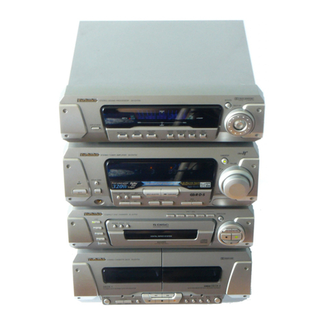
Technics SH-E5 User manual

ORDER
NO.
SD82062214c8
Service
Manual
Stereo
Graphic
Equalizer
OH-E5
[D],[EK],[EW],[EB],
[EF],[EGA],[EH],
[XA]
XL
]
SH-ES
(W)
]
[D],[EK],[
EW],
[EB],
[EF],[EGA],[EH],
[XA],[XL
*
[D]
is
available
in
Scandinavia.
*
[EK]
is
available
in
United
Kingdom.
*
[EW]
is
available
in
Switzerland.
*
[EB]
is
available
in
Belgium.
*
[EF]
is
available
in
France.
*
[EGA]
is
available
in
F.R.
Germany.
*
[EH]
is
available
in
Holland,
*
[XA]
is
available
in
Southeast
Asia,
Oceania,
Africa,
Middle
Near
East
and
Central
South
America.
*
[XL]
is
available
in
Australia.
*
The
cabinet
and
front
panel
are
available
in
black
color
and
silver
types.
*
The
black
type
model
is
provided
with
(K)
in
the
Service
Manual.
Specifications
(Specifications
are
subject
to
change
without
notice
for
further
improvement.)
(DIN
45
500)
Band
level
controls
:+12dB~-12dB
Frequency
response
(center
position)
:5
Hz~100
kHz,
—1
dB
(12
elements
continuously
variable
per
channel)
Maximum
output
Center
frequency
216
Hz,
31.5
Hz,
63
Hz,
125
Hz,
voltage
:
8V(1
kHz,
THD
0.01%)
250
Hz,
500
Hz,
1
kHz,
2
kHz,
Rated
output
voltage
:1V
4
kHz,
8
kHz,
16
kHz,
32
kHz
Rated
total
harmonic
distortion
:
0.005%
(20
Hz~20
kHz)
GENERAL
0.003%
(1
kHz)
Power
supply
:
AC
240
V
50
Hz
only
(For
Australia
Input
sensitivity
“1V
and
for
United
Kingdom)
Signal-to-noise
ratio:
100
dB
(110
dB,
IHF’
A)
AC
220
V
50
Hz
only
(For
Germany
Maximum
input
and
for
Switzerland)
voltage
:8V
(1
kHz)
AC
110
V/120
V/220
V/240
V,
Input
impedance
247kO
50
Hz/60
Hz.
(For
areas)
Gain
:0+1dB
Power
consumption
:17W
Channel
balance
Dimensions
250
Hz~6300
Hz
:+0.5dB
(HxWxD)
>50x315x240
mm
Channel
separation
(2’’X
12-13/32’’x
9-7/16"’)
1kHz
:60
dB
Weight
12.0
kg
(4.4
Ib)
B
CONTENTS
Page
Page
LOCATION
OF
CONTROLS
....................
2
SCHEMATIC
DIAGRAM...................0004
9
TOTAL
FREQUENCY
RESPONSE
................
3
EXPEODEDEVIEWE
tes
ee
os
a
a
ws
Go
ev
13
DISASSEMBLY
INSTRUCTIONS
.................
3
REPLACEMENT
PARTS
LIST
................00.4
15
BLOCK
DIAGRAM#ieclar..
<
.
cosecta
seesiecs
eee
ta
5
RESISTORS
&
CAPACITORS
...................
16
CIRCUIT
BOARDS
AND
WIRING
CONNECTION
DIAGRAM................000.
6
Matsushita
Electric
Trading
Co..
Ltd.
P.O.
Box
228,
Central
Osaka
Japan
‘Technics
li
LOCATION
OF
CONTROLS
Power
switch
Tape
monitor
(
M
source,
—
tape)
Equalization
switch
(EQ)
(
@
off,
=
on)
Equalization-position
Left
channel
band-level
control
Right
channel
band-level
control
switch
(position)
(16Hz
~
32kHz,
divided
into
(16Hz
~
32kHz,
divided
into
(
acu
rected)
12band
in
1
octave)
12band
in
1
octave)
(To
Amplifier)
LINE
IN
Direct
AC
outlet
connector
LINE
OUT
(unswitched)
=>
f=
iin
pie:
PLAYBACK
connector
REC
OUT
=
Voltage
selector
(From
Deck)
*
This
power
supply
for
this
unit
varies
depending
the
areas.
Also,
the
parts
use
for
power
supply
are
different.
So,
refer
to
the
circuit
diagram
and
replacement
parts
list.
*
[D],
[EB],
[EF],
[EH]
and
[XA]
areas
are
provided
with
voltage
selector.
as
Power
supply
circuit
Power
transformer.
;
a
Buffer/Operation
circuit,
muting
circuit
(
=)
a
:
oe
a
F
7
j
|
Right
channel
1
BPF
!
Se
J
i
iS
si
as
me
-
)
Ge
=I,
1!
|
D
i
i
i
“1
i
Left
channel
ae
)
nd
BPF
—)
cael
i}
1
ae
a
=
SS
i)
.
EF,
Vee
t |
0
)
/
0
|
f
i
|
:
()
0 (i
=
Bs
iis
ee
Ay
0
0
f)
4
Bisel
os
«
|
0
=
Ta
SSS
ss
NX
pci
oe
epee
ort
ae
aN
(L
dV,
‘
gaia
as
a
ae
(is gia
NP
ee
ee
ee
==
=
=
ee
:
oe
e
ie
Li
<
oo
CS
|
.
:
Cs
ss
LS
LL
.
La
Switch
circuit
Right
and
left
channel
band
level
control

Mi
TOTAL
FREQUENCY
RESPONSE
+12
+6
~
4
.
2%
Ss
SE
16
315
63
125
250 500
1k
2k
Frequency
(Hz)
li
DISASSEMBLY
INSTRUCTIONS
PWN
WON=—
@
iS
Setscrew
rf
Front
panel
Ss
LED
P.C.B.
setscrews
(3
pes)
Fig.
1
How
to
remove
the
front
panel
.
Remove
the
setscrew
(Fig.
1:
@
~
@),
and
then
the
cabinet
can
be
removed.
Shift
the
band
level
knobs
(24
pcs)
up
(+12dB).
Remove
the
3
setscrews
of
the
front
panel.
Release
the
claws(@
~
@)
at
top
of
the
front
panel
by
a
screwdriver.
Pull
the
front
panel
toward
you
with
care
not
to
scratch
the
knobs.
Remove
the
LED
P.C.B.
inside
the
front
panel.
Then
the
front
panel
can
be
removed.
Note:
When
remove
the
band
level
control
knobs,
remove
the
front
panel
first.
How
to
remove
the
P.C.B.
.
Remove
the
cabinet.
.
Pull
out
the
3
connectors
(J8,
9,
11).
.
Remove
the
rear
terminal
setscrews
(Fig.
2:
@,
@)
and
the
5
setscrews
(Fig.
2:
@
~
@
)
of
the
P.C.B.
.
Pull
the
P.C.B.
toward
you
and
lift
it.
Front
panel
Front
panel
4
4k
8k
16k
32k
Screw
driver
Y
Front
Panel
@
How
to
remove
the
slide
volume
1.
2
3
Remove
the
cabinet
and
front
panel.
Remove
the
2
setscrews
of
front
plate,
and
3
connectors
(J7,
10,
11).
(Fig.
3)
Remove
the
power
supply
knob.
Release
the
chassis
stopper
from
inside,
and
lift
the
front
plate
to
remove.
.
Pull
out
the
24
knobs
for
the
right
and
left
channels,
and
then
remove
the
film.
(Fig.
4)
Push
the
claw
of
the
ornament
from
inside
as
in
Fig.
4
to
remove
the
ornament.
(There
are
4
ornaments,
so
remove
the
other
orna-
ments
in
the
same
way.)
.
Remove
the
16
setscrews
of
the
slide
volume
and
remove
them
from
the
front
chassis
along
with
the
E:G:By
Ornament
Volume
setscrew
(16
pes)
Fig.
4
e
How
to
remove
the
direct
connector
1.
2
Remove
the
cabinet.
Remove
the
terminal
setscrews
(Fig.
6:
®@,
®)
and
6
setscrews
(Fig.
6:
@
~
@®)
of
the
rear
panel,
and
then
draw
out
the
rear
panel.
.
Pull
out
the
direct
connector
and
remove
it
in
the
the
numerical
order
@
~
©.
Power
supply
8
Front
plate
Lin
Chassis
Oe
Front
plate
setscrews
(2
pes)
Stopper
@
Release
by
screwdriver
e
How
to
set
the
film
Set
the
film
onto
each
volume
lever
with
the
face
(printed
side)
down
as
shown
in
Fig.
5.
Next,
fit
in
the
ornament
and
then
set
the
film
as
in
Fig.
5.
f
Printed
side
3
Volume
lever
Front
plate
plate
Ornament
Fig.
5
Direct
connector
®

li
BLOCK
DIAGRAM
4azj14
ssed
pueg
ZL
vel
—~
1010
ddd
pZlo
—~
lol
(493]1}
8010190
1)
ZHACE
~~
ZHO9I
po--a--
|
|
LiL
|
+
4a1j198H
1G
S2uy
9
a®
ao
(2/1)
191
BuryouiMg
(2A)
191
dwe
uolesado/saying
Sasa
ents
|
(uoi1isod
OF)
a94no0s
(S-2S)
©
40}99UU09
pasg
LNdLNO
/LNdNI
40}9UU0D
wag
©
[zno
ann]
[unooau]
[
avidoae
|

@
CIRCUIT
BOARDS
AND
WIRING
CONNECTION
DIAGRAM
Ground
(Earth)
Lines
TAPE
’
White
————
DIRECT
CONNECTOR
DIRECT
CONNECTOR
[LINE
IN]
[LINE
OUT]
[REC
OUT]
[PLAYBACK]
sige
Brown
®
Red
@
(
Yellow
Yellow
Power
transfor
Black
(TI)
——
left
channe|—
r——right’
channe|
——
=
B
=
ee
@
4
0
4
8
i
cee)
@-4£
o14
8
ge)
ae
Lb
bP
Perea
tera
iat
bf
sf
POWER
ah
ee
2
Ub
et
GROUND
POINT
bs
Lb
=
I
L*&oajit4
weld
L
J10

Ground
(Earth)
Lines
[—TAPE
—
ECT
CONNECTOR
[LINE
IN]
[LINE
OUT]
[REC OUT]
[PLAYBACK]
!
Waite
REC/PLAY
=
Orange
2
Brown
VOLTAGE
Red
SELECTOR
AC
OUTLET
Yellow
Brown
ae
Yellow
Power
transformer
|
|
Black
(Tt)
Blue
ial
AC
110/120/220/240V
(50/0Hz
)
Blue
GROUND
POINT
POWER
INDICATOR
fo)
awa,
Sf
S2
TAPE
E@
MONITOR]
POSITION

eS
SCHEMATIC
DIAGRAM
(
This
schematic
diagram
may
be
modified
at
any
time
with
the
development
of
new
technology.)
1
2
3
4
5
6
7
8
9
l
10
SUPK
498C
S3-1~$3-4
SUPK
498A
R13
150K
SUPK
498B
S2-tn
S2-4
cet
Sk
saa
LI
sss:
4
vas
POSITION)
IC
1,2
COM.
SVITA75559S
BUFF/OP.
AMP
A
LINE
IN
+15.2V
LINE
LINE
OUT
$4
mt
L
|
=
|
|
[o]
[
il
B
.
+o
3
Y
REC
OUT
=
x<
|
‘
:
Be
Ss
a
TAPE
a
z}
PLAY
aN
G
QIol
~
124
Ste
23
2502878
C304
C302
414
2SCI8I5L
ed
is
(4
nm
;
a=
oO
70
E
—14.4
C101
C201
g
25V3.3.
50V1
C113
C213
+¥
yt
/
R206
R406
D
INPUT,
S
OUTPUT
3
63Hz
Ss
R101
820
x
R105
820
R109
820
R121
820
R106
R501
R505
R50?
R521
R506
2.7K
C103.
=
C:203
——
2
50y
2.2
50V0.33
ii]
ee
Gor.
C207
+y
R208
=)
ao
E
Q
Ss
125Hz
9
~
3
R107
820
R111
820
R115
820
R123
820
R108
R319
10K
R507
R511
R515
R519
R523
R508
6.8K
G1)
G9)
C=
=O
=
Se”
ee
[ae
Se
Ga
Gane
SE
ee
ee
Soe
ee
ee
ee
S10
=a
S|
F
q
poe
Ue
Ue
1
—
SUPK
520B

10
11
12 13
14
15
16
D3,4
Q4
Q3
Ol
CIMAIIGOM
2SA968
2562238
g
SVDIB4B42
REGULATOR
REGUL
&
AXDic66
|
GROUND
POINT
At
(VOLTAGE
SELECTOR)
A
ea
Bale
F4
T200m
ac
ov"
TTRED
200
S.A
gg
R57
‘4wi0
oN
:
AN
F2._7200mA
+
©)
z
C57
25V
100
C55
(9)
BLK|
A
@
A
|
AC
50/60HZ
AC
on
110/120/220/240V
YEL!
A
R58
14W
10
C56
He.
C58
25V
100
(POWER)
—15.2V
LINE
et
Notes:
D9
*
The
part
No.
of
transistors,
IC
and
diodes
mentioned
in
the
schematic
diagram
stand
for
production
part
No.
Regarding
the
part
No.
with
©
mark,
the
production
part
L
N224
WP
No.
are
different
from
the
replacement
part
No.
Therefore,
when
placing
an
order
for
POWER
INDICATOR
replacement
parts,
please
use
the
part
No.
in
the
replacement
parts
list.
=
.
This
is
the
basic
circuit
diagram
(For
continental
Europe)
of
this
unit.
Note
that
part
of
the
circuit
is
subject
to
change
depending
on
the
areas,
2.
Regarding
the
circuits
to
be
changed
in
the
basic
circuit
diagram
(For
continental
Europe)
and
related
areas
[EK]
,
[EW]
,
[EGA]
and
[XL],
refer
to
speparated
service
manual
(Order
No.
SD82062214
C8—A).
3.
$1-1
~
$1-2
:
Tape
monitor
switch
in
“source”
position.
source
+
tape
4,
S$2-1
~
$2-6
:
Equalization
position
(position)
switch
in
“source’’
position.
source
@
rec
out
5.
S3-1
~
$3-4
:
Equalization
(EQ)
switch
in
“on”
position.
6.
SA
:
Power
switch
in
“on”
position.
7.
$5
:
Voltage
selector
switch
in
“220V”
position.
110V
+
120V
«
220V
©
240V
8.
The
R
and
L
channels
use
the
same
circuit.
For
the
resistance
and
capacity
of
R
channel,
refer
to
the
L
channel.
9.
Cc]
Indicated
voltage
values
are
the
standard
values
for
the
unit
measured
by
the
DC
electronic
circuit
tester
(high-impedance)
with
the
chassis
taken
as
standard.
There
fore,
there
may
exist
some
errors
in
the
voltage
values,
depending
on
the
internal
impedance
of
the
DC
circuit
tester.
10.
Signal
lines
of
left
channel.
11,
mmm
=
Positive
(+B)
voltage
lines.
=manp
Negative
(—B)
voltage
lines.
12.
Important
safety
notice:
Componetns
identified
by
A
mark
have
special
characteristics
important
for
safety.
When
replacing
any
of
these
components,
use
only
manufacturer’s
specified
parts.
a6
2SCl8I5
MUTING
PSA
1015
MA27\
MUTING
2
iC2878
ITCHING
25v220
+
TF
25V220
Cil0
=
=C210
C122
C222
102
C202
a
4
R202
I6Hz
R102
R502
C208
Cil2.
212
C116
C216
104
C204
t
ve:
C108
+¥
R204
e
Terminal
guide
of
transistors,
|C
and
diodes
31.5Hz
R104
SVITA75559S
2SA1015,
2SC1815,
2SA968,
SVDIB4B42
28C2827
2SC2238
MOUs
R504
MA162A
=
LN224wP
as
a
eee
ee
ul
es
5
—Ta—
|
16Hz
|
Sil
[31.512]
Z|
|
63Hz|
l125Hz|
|
250Hz|
1k
Hz
|
|
2kHz
|
|
&kHz_|
pr
ey
Cf
Oe
Ue
Cb
Ce
UP
Ue
7
20B

Hi
EXPLODED
VIEWS
*
*
*
Power
transformer
fy
AY
x
if
ml),
x
/
BUD
S
Y
{\S
Tk
\e—3W\a
\
See
5
Eee
Ly
CTD
{pS
==
Aa
\)
RTT
(i
GaSe
A
D'S
\&8
LY
Kp
\
LY]
WD
;
S
e977
<
Al
—
IU)
KY
i,
1S
5
5,
x;
R\
oF
gq.
‘
V
.
Lead
clamper
Connectors
e
Accessory
E
=
a
©
a
c
2
a
8
Ss
w
—
*
@
3)
©
©
i
ue
£
@
a
&
c<
>
©
2
*
EH]
is
available
in
Holland.
*
XA]
is
available
in
Southeast
Asia,
Oceania,
Africa,
*
Middle
Near
East
and
Central
South
America.
*
[XL]
is
available
in
Australia.

Mi
REPLACEMENT
PARTS
LIST
Mi
RESISTORS
&
CAPACITORS
Notes:
Notes:
1.
Part
numbers
are
indicated
on
most
mechanical
parts.
3.
The
‘S"
mark
is
service
standard
parts
and
may
differ
from
1.
Part
numbers
are
indicated
on
most
mechanical
parts.
Please
use
4.
The
‘’S’
mark
is
service
standard
parts
and
may
differ
from
Please
use
this
part
number
for
parts
orders.
Production
parts.
this
part
number
for
parts
orders.
production
parts.
2.
Important
safety
notice:
:
4.
Unless
otherwise
specified.
2.
Important
safety
notice:
5.
[®
-marked
parts
are
used
for
black
type
only,
while
Omarked
Components
identified
by
A
mark
have
special
characteristics
All
resistors
are
in
OHMS
(Q)
K
=
10009
,
M=
1000kQ
Components
indentified
by
A\
mark
have
special
characteristics
parts
are
for
silver
type
only.
important
for
safety.
When
replacing
any
of
these
components
All
capacitors
are
in
MICROFARADS
(xF)
P
=
uuF.
important
for
safety.
When
replacing
any
of
these
components,
6.
Parts
other
than
[)
and
O-marked
are
used
for
both
black
and
use
only
manufacturer's
specified
parts.
use
only
manufacturer's
specified
parts.
silver
types.
3.
Bracketed
indications
Ref.
No.
columns
specify
the
area.
7.
The
parenthesized
numbers
in
the
columns
of
description
N
. :
4
:
.
umbering
System
of
Resistor
Parts
without
these
indications
can
be
used
for
all
areas.
stand
for
the
quantity
per
set.
9
ey
7
System
of
Capacitor
xample
Black
type
model
No.
:
SH-E5
(K)
Example
ECKD
fi
102
=
ERD
25
F
J
101
Type
Voltage
Value
Tolerance
Peculiarity
Type
Wattage
Shape
Tolerance
Value
ECEA
50
M
R47
R
Description
Part
No.
Description
&
Pcs
Ref.
No.
Part
No.
Description
&
Pcs
(1/4)
(10082)
Type
Voltage
Peculiarity
use
Value
=
Special
use
INTEGRATED
CIRCUIT
SBC425—1
Button,
Power
Source
(1)
|
|
26[EK,XL]|
SMXA65
Cover,
Capacitor
(1)
50
Voltage
SBCK31
Button,
EQ
(1)
(C1001)
Wattage
Capacitor
Type
Tolerance
C1,
2
SVITA75559S_
|
Operation
SBCK31—1
_|
Button.
Tape
Monitor
(2)|
|
26
[Other]
|
SMXK26
Cover,
Capacitor
(1)
(1/2W)
ECEA
Type
—|_/Qthery
Amplifier
&
Position
(C1001)
SBDK4
Knob,
Band
Level
(24)
TRANSISTORS
Control
27
SMX663
Cover,
AC
Outlet
(1)
—
:
SGXK47—1
Ornament,
Band
Level
(4)
|
|
28
SJT347
Holder,
Fuse
[Other]
(4)
2SC2878A—T
|
Switching
Volume
[EW,EGA]
(6)
2SC2238—OLB
|
Regulator,
SDUK5—1
Filme
@B
Voltage
SUBK6
Coupling
Rod
SCREWS
2SA968—OLB_
|
Regulator,
N1
S
|
XTN3+8B
Tapping,
©
3x
8
©B
Voltage
9
(EK.XL,
|
SKUKHE5N
Bottom
Board
,
W/Feet
N2
XTB26+
6B
Tapping,
©26x
6
2SC1815L—G
|
Muting
Circuit
EW.EGA)
N3
XSN3+6S
@®3x6
Q7
2SA1015L—G
|
Muting
Circuit
9
[Other]
|
SKUKHE5D
Bottom
Board,
W/Feet
N4
XSN2+4
@2x4
Q101~124
2SC1815L—G
Band
Pass
Filter
N5
XTBS3+
8BFZ1|
Tapping,
@3x
8
10
SKL245—2
Foot
N6
XTB3+8BFN
|
Tapping,
63x
8
11
SJF3055—1N
Terminal,
Output
&
N7
XTN38+10B
Tapping,
®3x
10
Input
N8
XTN3+10BFZ
|
Tapping,
®3x
10
NQ
XTB3+10BFZ
|
Tapping,
®3x
10
Electrolytic
1A:
10V
|}
1H
=:
S5SOVDC
:
£5%
Ceramic
1E
:
25V
05
:
50V
:
+
10%
Ceramic
1V:
35V
KC
:
400VAC
:
+80%,
—20%
Polyester
1H
:
50V
:
+100%,
—0%
TF
50
:
50V
25
:
25V
Ref.
No.
PartNo.
Ref.
No.
Part
No.
R201,
202
ERD25TJ473
R203,
204
ERD25TJ563
Care
clTOn?
R205,
206
ERD25TJ104
C13,
14
S$
|
ECCD1H680K
R207,
208
ERD25TJ563
(EGA)
only
R209,
210
ERD25TJ104
C15,
16
S$
|
ECCD1H680K
R211,
212
ERD25TJ473
(EGA)
only
R213,
214
ERD25TJ563
C1,2
R215,
216
ERD25TJ563
C3,
4
R217,
218
ERD25TJ563
C5,
6
R219,
220
ERD25TJ563
C78
C9,
10
ERD25TJ563
C11,
12
ERD25TJ563
C51,
52
ERD25FJ103
C53,
54
ERD25TJ154
C55,
56
ERD25TJ104
C57,
58
ERD25FJ272
ERD25FJ272
C59,
60
ERD25FJ272
C61
ERD25FJ272
C62
ERD25FJ272
C63
C64
ERD25FJ272
C65
ERD25FJ272
C66,
67.
A
ERD25FJ682
C101,
102
ERD25FJ682
C103,
104
ERD25FJ682
C105,
106
ERD25FJ682
ERD25FJ682
C107,
108
ECEA50ZR33
ERD25FJ680
C109,
110
ECQM1H184KZ
ERD25FJ221
C111,
112
ECQM1H104JZ
ERD25FJ331
C113,
114
ECQM1H473JZ
C115,
116
ECQM1H223JZ
ERD25FJ680
C117,
118
ECQM1H123JZ
ERD25FJ221
C119,
120
ECQM1H562JZ
ERD25FJ221
C121,
122
ECQM1H272JZ
ERD25FJ221
C123,
124
ECQM1H122JZ
ERD25FJ181
C201,
202
ECEA50Z1
ERD25FJ151
ERD25FJ680
C208,
204
ECEA50ZR33
ERD25FJ101
C205,
206
ECQV05154JZ
ERD25FJ680
C207,
208
ECQV05124JZ
C209,
210
ECQM1H563JZ
C211,
212
ECQM1H273JZ
C213,
214
ECQ@M1H123JZ
C215,
216
ECQM
1
H682JZ
C217,
218
ECQM1H332JZ
Ref.
No.
Part
No.
C219,
220
ECQM1H152JZ
C221,
222
ECKD1H821KB
C223,
224
ECKD1H471KB
C301,
302
ECEA1ES220
C303,
304
ECEA1ES220
c1i001
«A
ECKDKC103PF
RESISTORS
R7.
8
S
|
ERD25FJ102
(EGA)
only
RQ,
10
S$
|
ERD25FJ102
{EGA}
only
R11,
12
R13,
14
R15,
16
R17,
18
R19,
20
R23,
24
R25,
26
R27,
28
R29,
30
R31,
32
SVD1B4B42
Rectifier
(Ew)
|
SGPK140—1B
|
Rear
Panel
MA162A
Rectifier
(EGA)
|
SGPK140—1C
|
Rear
Panel
N10
=
_O|
SNE2095—2
|
Cabinet,
(Silver)
SVDRD16EB
Zener,
16V
(EK)
SGPK140—2A
|
Rear
Panel
N10
Lo
SNE2095—3
Cabinet,
(Black)
MA162A
Switching
x
SGPK140—3A
|
Rear
Panel
MA162A
Rectifier
[Other]
|
SGPK140—1A
|
Rear
Panel
N11
S
|
XTB3+10BFZ
|
Tapping,
©3x
10
MA27W—A
Switching
LN224wP
Power
Indicator
A
|
SJS9227
Socket,
AC
Outlet
WASHERS
(EK)
only
13
A
|
SJS9225
Socket,
AC
Outlet
Spring.
$3
7
14
SHR127
Bushing,
AC
Cord
EVAH36P18G25
|
Band
Level
Control,
15
(EK)
A
|
SJA149
AC
Cord
PACKING
PARTS
200k2(G)
15
(XL)
A
|
QFC1208M
AC
Cord
P1
(EK,.XL)|
SPGK97
Carton
Box
15
A
|
SJA151
AC
Cord
P1(EF)
|
SPGK96
Carton
Box
TRANSFORMER
[Other]
P1
[Other]
|
SPGK95
Carton
Box
SJS9605
Direct
Connector,
T1
(EK,XL)
4
|
SLTK5J11—W
|
Power
Source
Input/Output
P2(EK,xL)|
SPSK43—1
Pad,
Front
Tl
[EW,EGA]
4
|
SLTK5J12—W__|
Power
Source
SJS9607
Direct
Connector,
P2
[Other]
|
SPSK43
Pad,
Front
T1
[Other]
4]
SLTK5U8—W__
|
Power
Source
Rec/Play
ERD25TJ154
ERD25TJ154
ERD25TJ333
ERD25TJ104
ERD25TJ154
ERD25FJ102
ERD25FJ822
ERD25FJ103
ERD25TJ104
ERD25TJ104
ECEA25Z4R7
ECCD1H101K
ECCD1H101K
ECCD1H101K
ECEA25Z4R7
ECEA1AS101
ECEA1VS102
ECEA1ES101
ECEA1ES101
ECEA1ES101
R221,
222
R223,
224
R319,
320
R405,
406
R409,
410
R501,
502
R503,
504
R505,
506
R507,
508
R509,
510
ANDNDDNDARNRDHAAnANH
ANNDNNDHURnDAN
R33,
34
R35,
36
R37,
38
R39,
40
R41,
42
ERD25TJ154
ERD25FJ822
ERD25FJ222
ERD25TJ104
ERD25FJ102
ERD25FJ181
ERD25FJ681
ERD25FJ391
ERDSOFJ100
ERD50FJ100
ECEA1ES221
ECEA1VS101
ECEA50Z1
ECEA1ES101
ECEA1HS100
ECEA1HS100
ECKD1
H103ZF
ECEA50Z3R3
ECEA50Z2R2
ECEA50Z1
ANDNADNHRUADRNDAUNDDHARVRHVURADUAUHDHRAHGRDAnN
P3(EK,XL)|
SPSK44—1
Pad,
Rear
SKCKHE5N
Cabinet
(Silver)
P3
[Other]
|
SPSK44
Pad,
Rear
FUSES
SKCKHE5KD
Cabinet
(Black)
R511,
512
R513,
514
R515,
516
R517,
518
R519,
520
R521,
522
R523,
524
R601,
602
R603,
604
R605,
606
R43,
44
R51,
52
R53,
54
R57,
58
R59,
60
ANNNNHAUAHnNH
P4
O
|
SPP691—1
Polyethylene
Bag,
F1,2
A
|
XBA2CO2TRO
[Beate
250V
SJT783
Terminal,
Socket
(Silver)
F3
(EW,EGA)
A
|
XBA2C12TRO
T1.25A,
250V
P4
Lo
SPP713
Polyethylene
Bag,
only
$JS5331
Socket
(3
Pin)
(Black)
SJS5425
Socket
(4
Pin)
SWITCHES
SJS5629
Socket
(6
Pin)
P5
SPHK17
Polyethylene
Sheet
SJS5047
Socket
(15
Pin)
P6
SGK1413
Label,
(Black
Type
$1,
2
SSHK23
EQ@
Position,
Tape
take
fa
SJT3319
Connector
(3
Pin)
ontyy
$3
SSHK22
EQ
SJT3415
Connector
(4
Pin)
S4
A
|
ESB90619S
Power
Source
SJT3611
Connector
(6
Pin)
ACCESSORIES
$5
[D.XA,EB,
A|
ESE3787
Voltage
Selector
SJT3027
Connector
(15
Pin)
A1(XA.XL)|
SQFK10014
__|
Instruction
Book
EF,EH]
only
A1[Other]
|
SQFK10015
Instruction
Book
BPR
Bb
aon
DDDDDDDHOOD
77)
R61
R62
R63
R64
R65
R66
R101,
R103,
R105,
R107,
ERD25FJ472
ERD25TJ183
ERD25FJ222
ERD25FJ562
ERD25FJ103
ERD25FJ102
ERD25FJ821
ERD25FJ821
ERD25FJ821
ERD25FJ821
ANNHRNDAHRVNRARADnA
R607,
608
R609,
610
R611,
612
R613,
614
R615,
616
R617.
618
R619,
620
R621,
622
R623,
624
ANNNHANDNARNRNAAnAN
HRNNHRHHHAAnANH
SJS5519
Connector
(5
Pin)
Ref.
No.
Description
&
Pcs
SJS5627
Connector
(6
Pin)
a“
R109,
R111,
R113,
R115,
R117,
R119,
R121,
R123,
ERD25FJ821
ERD25FJ821
ERD25FJ821
ERD25FJ821
ERD25FJ821
ERD25FJ102
ERD25FJ821
ERD25FJ821
°
Pi
CABINET
and
CHASSIS
PARTS
SWKKHES—2
|
Lead
Ass'y
ve
peat
spias
1
O
|
SGWK120A
Front
Panel
Ass‘y
(1)
SHE135
Pin
(Silver)
(Silver)
|
ig
ae
1
BEN
SGWK120BA
|
Front
Panel
Ass'y
(1)
SHE135—1
in
(Black)
(Black)
SHR301
Clamper,
Lead
Wire
ANRNNAHNHDAAnN
ANNNNHVAAnAN
Printed
in
Japan
82069500
®
TK

Stereo
Graphic
Equalizer
GSH-E5/GH-
E5\(k)
This
booklet
contains
the
specifications
for
SH-E5,
written
in
Germany,
France
and
Spanish,
and
the
circuits
to
be
changed
according
to
the
areas.
ORDER
NO.
SD82062214C8—A
DEUTSCH
File
this
manual
together
with
the
SH-E5
service
manual
(Order
No.
SD82062214C8).
(DIN
45
500)
Frequenzgang
(mittelstellung)
Maximalausgangs-
spannung
Nennausgangsspan-
nung
Nennklirrfaktor
Eingangsspannung
Gerauschabstand
Maximaleingangs-
spannung
Eingangsimpedanz
Verstarkung
Kanalsy
mmetrie
250
Hz~6300
Hz
Kanaltrennung
1kHz
Mi
CARACTERISTIQUES
(DIN
45
500)
Courbe
de
réponse
(position
centrale)
Tension
de
sortie
maximale
Tension
de
sortie
nominale
Distortion
harmonique
totale
Sensibilité
d’entrée
Signal/Bruit
Tension
d’entrée
maximale
impédance
d’entrée
Gain
Equilibrage
de
canal
250
Hz~6300
Hz
Séparation
de
canal
1
kHz
DEUTSCH
Be)
TECH
N
ISCH
E
DATE
N
(Spezifikationen
Kénnen
infolge
von
Verbesserungen
ohne
Ankiindigung
gedndert
werden.)
:5
HzZ~100
kHz,
—1dB
:8V
(1
kHz,
THD
0,01%)
:1V
:0,005%
(20
Hz~20
kHz)
0,003%
(1
kHz)
SV:
:
100
dB
(110
GB,
IHF,
A)
:8V
(1
kHz)
247
kO
:0+1dB
:+0,5dB
760dB
7
RYN
NKOyAVES
Frequenzgangregler
:+12dB~-—12dB
(12
Regler,
stufenlos
verstellbar)
:
16
Hz,
31,5
Hz,
63
Hz,
125
Hz,
250
Hz,
500
Hz,
1
kHz,
2
kHz,
4
kHz,
8
kHz,
16
kHz,
32
kHz
ALLGEMEINE
DATEN
Stromversorgung
:
Wechselstrom,
240
V,
50
Hz
nur
(Fur
Austral
und
fur
England)
Wechselstrom,
220
V,
50
Hz
nur
(Fur
Deutsch
und
fur
Schweizerisch)
Wechselstrom,
110
V/120
V/220
V/
240
V,
50
Hz/60
Hz
(Fir
andere
Larder)
Leistungsaufnahme
:17W
Abmessungen
(Hx
BxT)
Mittenfrequenzen
:
50x315x240
mm
(2”’X
12-13/32”’
x
9-7/16"’)
Gewicht
:
2.0
kg
(4.4
Ib)
FRANCAIS
:5
Hz~100
kHz,
—1dB
:8V
(1
kHz,
THD
0,01%)
:1V
:0,005%
(20
Hz~20
kHz)
0,003%
(1
kHz)
:1V
:
100
dB
(110
dB,
IHF’
A)
:8V
(1
kHz)
247kO
:0+1dB
:+0,5
dB
:60
dB
(Sujet
4
changement
sans
préaris.)
Commandes
de
niveau
de
gamme
>+12dB~—12dB
(12
éléments,
continuellement
variables)
Fréquences
charniéres
:
16
Hz,
31,5
Hz,
63
Hz,
125
Hz,
250
Hz,
500
Hz,
1
kHz,
2
kHz,
4
kHz,
8
kHz,
16
kHz,
32
kHz
GENERALITES
Alimentation
:
CA.
240
V,
50
Hz
seul
(Pour
Australie
et
pour
Angleterre)
CA.
220
V,
50
Hz
seul
(Pour
Allemagne
et
pour
Suisse)
CA.
110
V/120 V/220
V/240
V,
50
Hz/60
Hz
(Autres)
Consommation
:17W
Dimensions
(hxIxpr)
mm
>50X315x240
mm
(2’’x
12-13/32”
x
9-7/16’’)
Poids
:
2,0
kg
(4,4
Ib)

ESPANOL
Respuesta
de
frecuencia
(posicidn
central)
Tension
de
salida
maxima
Tension
de
salida
de
régimen
Distorsion
armonica
total
nominal
Sensibilidad
de
entrada
Relacion
de
senal
ruido
Tension
de
entrada
maxima
Impedancia
de
entrada
Ganancia
Equilibrio
de
canales
250
Hz~6300
Hz
Separacion
de
canales
1
kHz
ESPANOL
4
ESPECIFICACION
ES
(Estas
especificaciones
est4n
sujetas
a
cualquier
cambio
sin
previo
eviso.)
(DIN
45
500)
:5
Hz~100
kHz,
—1dB
:8V(1
kHz,
THD
0.01%)
:1V
:0,005%
(20
Hz~20
kHz)
0,003%
(1
kHz)
7a
V,
:
100
dB
(110
dB,
IHF’
A)
:8
V
(1
kHz)
247kO
:0+1dB
:+0,5dB
>
60
dB
Controles
de
nivel
de
banda
Frecuencia
central
EN
GENERAL
Alimentacion
de
corriente
Consumo
de
corriente
Dimensiones
(alto
x
anchox
prof.)
Peso
Hi
CIRCUITS
TO
BE
CHANGED
AND
THE
AREAS
>+12dB~-12dB
(12
elementos,
continuamente
variables)
>
16
Hz,
31,5
Hz,
63
Hz,
125
Hz,
250
Hz,
500
Hz,
1
kHz,
2
kHz,
4
kHz,
8
kHz,
16
kHz,
32
kHz
:C.A.
de
240
V,
50
Hz
solo
(Para
Australia
y
para
Inglaterra)
C.A.
de
220
V,
50
Hz
solo
'
(Para
Alemania
y
para
Suizo)
C.A.
de
110
V/120
V/220
V/240
V,
50
Hz/60
Hz
(Para
otros
paises)
:17W
*
50315240
mm
(2”"x12-13/32”
x9-7/16"”
:
2,0
kg
(4,4
Ib)
e
Power
source
circuit
[XL]
area
F2
T200m
AC
240V
(50Hz)
[EK]
area
Ci001
20.01
[os
(POWER)
=
ve
Ee
>
So
oO
=
AC
240V
<
(50Hz)

[EW,
EGA]
area
Fi
T200mA
4
(POWER)
AC
OUTLET
AC
220V
(50/Z0Hz
)
Notes
:
*
[XL]
is
available
in
Australia,
*
[EK]
is
available
in
United
Kingdom.
*
[EW]
is
available
in
Switzerland.
*
[EGA]
is
available
in
F.R.
Germany.
e
Input
terminal
circuit
[EGA]
area
only
*
[EGA]
is
available
in
F.R.Germany.
_}
Additional
parts
f
REC
OUT
TAPE
This manual suits for next models
1
Table of contents
Other Technics Recording Equipment manuals

Technics

Technics SH-8028 User manual

Technics
Technics SY-FD20 User manual

Technics
Technics SH-8055 User manual

Technics
Technics SH-8065 User manual

Technics
Technics SH-DV250 User manual

Technics
Technics SH-DV280EG User manual

Technics
Technics SH-8029 User manual

Technics
Technics SH-EH50 User manual

Technics
Technics SH-DV290EG User manual

Technics
Technics SH-8029 User manual