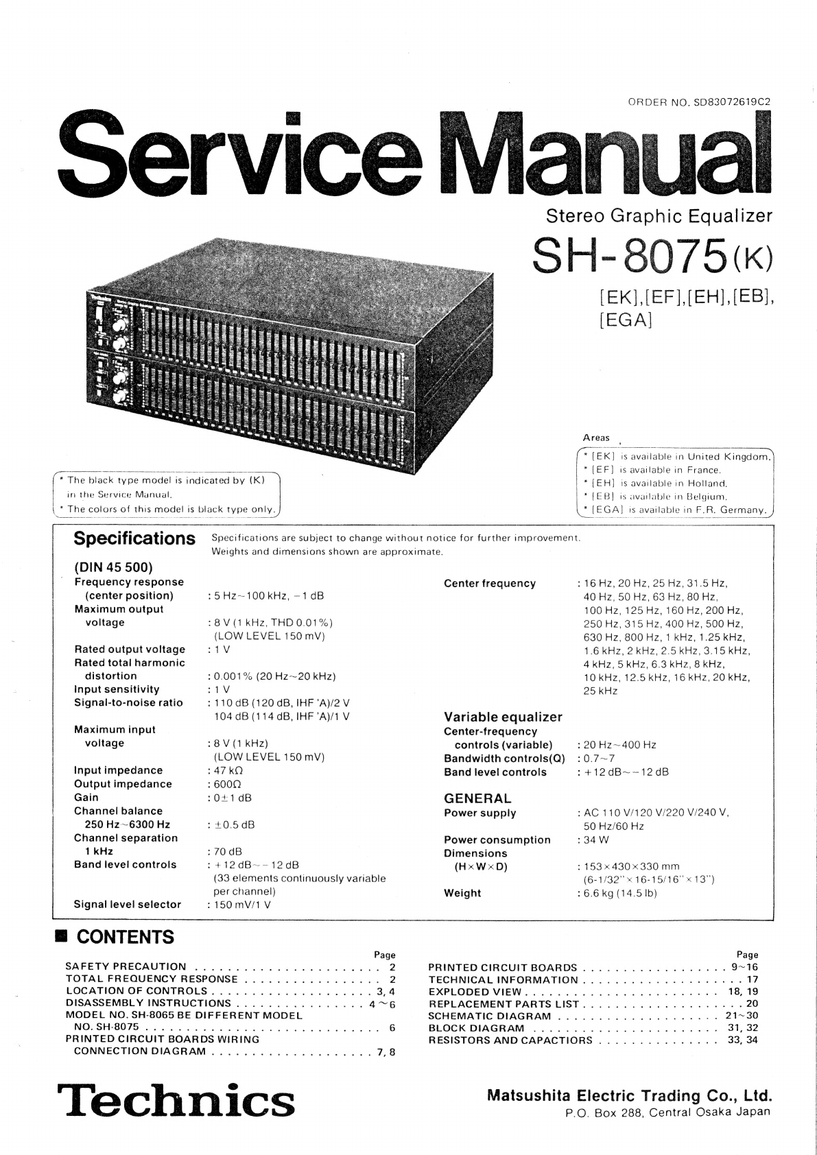
Technics SH-8075 User manual

|
\*
i
The
Bleek.
type
model
is
‘indicated
by
(K)
in
the
Service
Manual.
The
colors
of
this
model
|
1S
black
type
only.
"Naseperoctumsateleotinmnctoaity
cman
a
peta
in
ss
He
aces
Specifications
(DIN
45
500)
Frequency
response
(center
position)
Maximum
output
voltage
Rated
output
voltage
Rated
total
harmonic
distortion
Input
sensitivity
Signal-to-noise
ratio
Maximum
input
voltage
input
impedance
Output
impedance
Gain
Channel
balance
250
Hz~6300
Hz
Channel
separation
1
kHz
Band
level
controis
>5
HZ~100
kHz,
—1
dB
>8V
(1
kHz,
THD
0.01%)
(LOW
LEVEL
150
mV)
ames
>
0.001%
(20
Hz~20
kHz)
a
110
dB
(120
dB,
IHF
‘A)/2
V
104
dB
(114
dB,
IHF
’A)/1
V
8
V
(1
kHz)
(LOW
LEVEL
150
mv)
>
47
kQ
>
600Q
>O0+1dB
=+0:506
:70dB
+12dB~-12dB
Stereo
Graphic
Equalizer
Specifications
are
subject
to
change
without
notice
for
further
improvement.
Weights
and
dimensions
shown
are
approximate.
Center
frequency
ORDER
NO.
SD83072619C2
Areas
|,
[EH],
[EB],
*
EK]
is
cAvailieal
in
United
Kingdo
*
[EF]
is
available
in
France.
*{EH]
is
available
in
Holland.
*
(EB)
is
available
in
Belgium.
x
[EGA]
iS
available
in
F,
R.
Germ
an
a
TOA
202.
25
AZ
OV
oases
40
Hz,
50
Hz,
63-H2,:80:
Hz,
100:HZ,.125
Hz,
160
Hz,
200
Hz,
250
Hz.375-Hz,
400
Hz,.500
Hz,
630
Hz,
800
Hz,
1
KHz,
1.25
kHz,
16
KHz,
2
kHz;
2.5
KHZ,
3.15
kHz,
4
kHz,
5
KHz,
6.3
KHz,
8
KHz,
10
kHz,
12.5
KHz,
16
KHz,
20
kHz,
25
KHz
Variable
equalizer
Center-frequency
controls
(variable)
>
20
Hz~
400
Hz
Bandwidth
controls(Q)
:0.7~7
Band
level
controls
hie
dB]
1208
GENERAL
Power
supply
>
AC
110
V/120
V/220
V/240
V,
50
Hz/60
Hz
Power
consumption
>
34
W
Dimensions
(33
elements
continuously
variable
per
channel)
Signal
level
selector
7150
mV/1
V
&
CONTENTS
Page
SAFETY:PRECAUTION
2p
pei
ee
ERE
Baws
Seem
2
TOTAL
FREQUENCY
RESPONSE
ii
Bi
ity
Seah
Gas
Hes
hae
Cie
SO
aera
ean
LOCATION
OF
CONTROLS
.
Sk
WR
ote
lelctan
Woe
a
Ae
Ge
DISASSEMBLY
INSTRUCTIONS
.
;
fay
8k
ena
a
Oe
MODEL
NO.
SH-8065
BE
DIFFERENT
MODEL
NO.
SH-8075
:
:
ews:
&.
pay
“6
PRINTED
CIRCUIT
BOARDS
WIRING.
CONNECTION
DIAGRAM
i
a
iat
Bye
‘Technics
(HxWxD)
>
153x430
x
330
mm
(6-1/32"
«
16-15/16"
x
13")
Weight
:
6.6
kg
(14.5
Ib)
Page
PRINTED
CIRCUIT
BOARDS
..................
9°16
TECHNICAL
INFORMATION
.
ee
ee
ee
eee
|
EXPLODED
VIEW.......
le
18,19
REPLACEMENT
PARTS
LIST
.
Bi
eae
ole
ee
ea
ee
SCHEMATIC
DIAGRAM
..............
000-5.
21~30
BLOCK
DIAGRAM
.....
Say
&
bre
&
i
oe
SG
eee
RESISTORS
AND
CAPACTIORS
Pg
yk
he
BB
eA
Hata
ie,
Op
OA
Matsushita
Electric
Trading
Co.,
Ltd.
P.O.
Box
288,
Central
Osaka
Japan

B
SAFETY
PRECAUTION
mf
WN
-
Wh
-
©
_
Before
servicing,
unplug
the
power
cord
to
prevent
an
electric
shock.
.
When
replacing
parts,
use
only
manufacturer's
recommended
components
for
safety.
_
Check
the
condition
of
the
power
cord.
Replace
if
wear
or
damage
is
evident.
.
After
servicing,
be
sure
to
restore
the
lead
dress,
insulation
barriers,
insulation
papers,
shields,
etc.
.
Before
returning
the
serviced
equipment
to
the
customer,
be
sure
to
make
the
following
insulation
resistance
test
to
prevent
the
customer
from
being
exposed
to
a
shock
hazard.
INSULATION
RESISTANCE
TEST
.
Unptug
the
power
cord
and
short
the
two
prongs
of
the
plug
with
a
jumper
wire.
|
.
Turn
on
the
power
switch.
.
Measure
the
resistance
value
with
ohmmeter
between
the
jumpered
AC
plug
and
each
exposed
metal
cabinet
part,
such
as
screwheads
antenna,
control
shafts,
handle
brackets,
etc.
Equipment
with
antenna
terminals
should
read
between
3M22
and
5.2MQ
to
all
exposed
parts.
(Fig.
A)
Equipment
without
antenna
terminals
meule
read
approximately
infinity
to
all
exposed
parts.
(Fig.
B}.
Note:
Some
exposed
parts
may
be
isolated
from
the
chassis
by
design.
These
will
read
infinity:
Antenna
terminal
Exposed
metal
part
Ohmmeter
Ohmmeter’
(Fig.
A)
(Fig.
B)
Resistance
=
3M2
~
5.2M@Q
Resistance
=
Approx
OO
.
1f
the
measurement
is
outside
“he
specified
‘limits:
there
is
a
possibility
of
a
shock
hazard
The
equipment
should
be
saps
and
rechecked
before
it
is
returned
to
the
customer.
heed
@
TOTAL
FREQUENCY
RESPONSE
Frequency
response
(+12dB
position}
+12
poeta
ee
ee
ee
alee
die
2th
+10
PAAR
RAO
TAA
UTA
AA
wa
<p
PANINI
LIE
tee
oe
CONES
An
44
Ht
AAR
A
AAU
A
A
“4215
LL
A
AX
MARA
SAX
ee
Nrenuniel
0
ee
SSS
2
RAAT
OP
I
I
IO
ODI
AY
ALLA
—
4
DANO
MAK
KY
MY
TY
IXY
YI
TY
XIX
KAY
XX
AL
VARY
YY
yYVV
VV
YY
Vi
3
vuUW
Uh
ed
ori
a
SOFA
TA
A
TA
WUT
LT
A
“10
23.
§
7100
2.3
§
71%
23
5710k
23
§
Frequency
(H2)
Level
a

SH-8075
@
LOCATION
OF
CONTROLS
Power
switch
©
Band
ievel
control
Equalizer
on/of*
switch
|
B
oft,
=
on}
Recording
mode
switch
{
Mf
straight,
=
EQ)
tape
7
tase
2
@
Sand
level
contro!
@
Bandwidth
{Q)
control
©
Variable
equalizer
switch:
Lch.
{
EE
off,
=
on)
@
Bandwidth
(Q)
contral
Band
jevel
controls
:
L
ch,
+12d8
@
Frequency
control
{Hz)
Band
level
controls
:
R
ch.
+12dB
@
Frequency
control
(Hz)
@
Variable
equalizer
switch
:
Rich.
(
M
off,
=
on)
input
selector
input
signal
level
saleetec
@
VARIABLE
EQUALIZER
os
“Technica:
Information”
on
page
17
also
describes
me)
variable
equalizer.
The
variable
2qualizer
can
be
used
for
corrections
of
low-frequenc.
characteristics.
The
functions
in
this
unit
are
as
follows:
@
Center
frequency
contro!
knob
(frequency,
Hz)
is
able
to
cantinuously
vary
the
frequency
in
a
range
Of
20Hz
~
400Hz
to
set
it
to
the
desired
point.
@
Band
width
knob
fhandwidth.
O)
ie
able
to
conti-
hudusly
.aty
the
resonance
peak
{Q)
of
frequency
set
by
knob
6
@_
in
a
range
of
0.7~7.
Turning
it
counters
7ckwise
decreases
the
value
of
Q,
making
H
9a
te
ri
a
a
an
an
Ahn
Sie
ma
To
©
iets
A
hab
fs
dee
rh
MN
wate
on
LINE
IN
!
——PLAYBACK
=
:
ae
Dba
eh
I
To
Tape
deck
2
Pa
REC
OUT
el
cae
sn
4
PLAYBACK—————y
=
-
Low
level
~
150m
V
side
{Input
from
“REC
OUT"
of
amplifier:
Output
to
“"PLAYBACK"’)
High
level
>
1V
side
(Input
from
“PRE
OUT"
of
amplifier
:
Output
to“MAIN
IN’)
Voltage
setector
(110V/120V/220V/240V)
=
To
Tape
deck
1
the
peak
and
dip
gentle,
while
turning
it
clockwise
increases
the
value
of
Q,
making
the
peak
and
dip
sharp,
resulting
in
less
interference
given
by
or
to
adjacent
channels.
©)
Variable
equatizer
band
level
control
is
able
to
vary
the
frequency
set
by
knob
@
by
+12
dB.
If
the
frequency
set
by
knob
@
is
63
Hz,
then
it
can
be
varied
+24
dB
by
using
the
knob
@
and
the
22-division
GB
Hz
band
terel
conirel
Kage.
4)
Variable
equalizer
switch
(variable
£Q)
is
a
switch
to
turn
on/off
the
control
knobs
@
~
@.
(16H2~25kHz,
divided
into
33
band
in
1/3
octave.)
(16Hz~25kHz,
divided
into
33
band
in
1/3
octave.)
ook
Sa
S29
@®
OTHER
SWITCHES
*
Equalizer
on/off
switch
(EQ)
This
switch
is
used
to
turn
on/off
the
equalizer
circuit.
With
it
set
to
“on”,
the
frequency
characteristic
can
be
varied
by
the
upper
and
lower
band
level
controls
(33
sets
each)
and
the
variable
equalizer
band
level
controls
(1
set
gach)...
hy
Bas
*
With
Jit:
‘set,
to,
"off
“a
signal
is.
‘obtained
not
to
make
%
“off,
the
signal
comes
out
through
the
unit.
*
Record
mode
switch
(rec
mode)
When
recording
on
a
tape
deck,
correction
mode
is
selected
by
this
switch.
“EQ”
is
the
position
for
recording
with
correction
given,
@
DISASSEMBLY
INSTRUCTIONS
@
How
to
remove
the
bottom
board
.
Remove
the
8
setscrews
{red)
as
in
[Fig.
1]
to
reomve
the
bottom
board.
*Remove
the
bottom
board
from
andenesih
the
front
pane!
as
shown
by
the
arrows.
a
Red
‘<
(8
pes)
pte
oi
Input
selectar
switch
:
1
ie,
“Source”
is
the
position
“for
record
say:
and
radio
‘broadcast.
%
2
>
#
,
“equalizer
cotrection.4
flan
a7
*
Even
when
power
switch
is
off
with
this
switch
turned
yee
lf
the
equalizer
on/off
switch
is
set
to
“off’’,
the
“straight”
indicator
lights
up
and
signal
without
correc-
tion
will
be
recorded.
“Straight”
is
the
position
for
recording
without
correc-
tion
sae
“tape
1”
is
the
position
for
playback
on
a
tape
deck
connected
to
“TAPE
1°
terminal
on
the
rear
chassis
or
for
dubbing
from
tape
deck
1
to
2.
“tape
2”
is
the
position
for
playback
on
tape
deck
2
or
for
dubbing
from
tape
deck
2
to
1.
How
to
remove
the
front
panel
1.
Remove
the
setscrews
@
~
@
[Fig.
2]
to
remove
the
cabinet.
2.
Remove
the
5
setscrews
[Fig.
2]
of
the
front
panel.
3.
Pull
out
the
6-pin
connector
{terminals
@
~
@]
from
the
switch
P.C.B.
on
the
left
side.
[Fig.
3]
4.
Remove
the
front
panel
with
care
not
to
scratch
the
knobs.
Power
switch
and
bottom
connecting
rod
Pull
out
the
connector
before
removing
the
front
panel.
Front
panet
~—
Panel
setscrews
(5
pes)
Fig.
2

®
How
to
remove
the
band
level
controj
P.C.B.
if
2:
3;
Remove
the
front
panel.
Remove
the
band
level
contro!
knob.
(The
light
guide
plate
is
removed
with
it.)
Remove
the
light
shielding
cloth.
[Fig.
4]
_
Remove
the
9
setscrews
which
secure
the
R
or
L
channel
P.C.B.
[Fig.
5}
.
Remove
the
band
level
control
P.C.B.
*Each
control
LED
is
inserted
into
the
volume
lever
with
longer
pin
side
down.
Setscrews
af
switch
P.C.B.
(4
pes.)
P.C.B.
of
teft
ch.
band
level
contro!s
Light
guide
plate
Knob
\
epe
Light
guide
plate
Knob
2
insert
with
long
leg
down,
Ss
Setscrews
of
rith
ch.
band
fevei
control
P.C.B.
{9
pes.)
Fig.
5
@
How
to
remove
the
switch
P.C.B.
and
variable
equalizer
P.C.B.
1.
Remove
the
front
panel.
2.
Remove
the
4
setscrews
of
switch
P.C.B.
[Fig.
5].
3.
Pull
out
the
switch
P.C.B.
fixing
pin
[Fig.
8].
4.
Remove
the
6-pin
[terminals
(43)
~
(48)
]
and
7-pin
[terminals
(37)
~
(42)
]
connectors
from
the
variable
equalizer
P.C.B.
and
then
remove
the
switch
P.C.B.
as
in
Fig.
6.
5.
Check
the
P.C.B.
as
shown
in
Fig.
7.
Variable
equalizer
P.C.B.
Switch
P.C.B.
connector
6-pin
;
~
as
jy
7-pin
connector
SS
ACH
L
ua
TRRD
Woy
ass
ay
Power
supply
circuit
After
repair,
keep
the
lead
wire
away
from
the
power
supply
circuit.
Fig.
8
s
F
After
repair
a
Button
of
power
Push
switch
buttons
Level
control
knobs
1.
Make
the
wiring
away
from
the
power
supply
switch
knob
bight
guide
circuit
as
in
Fig.
8.
plat
2.
Be
sure
to
fit
each
button
and
switch
in
correct
positions.
[Fig.
9]
.
3
.
Side
down
Side
down
Gate
hole
side
of
malding
;
should
be
down.
Fig.
9
m@
MODEL
NO.
SH-8065
BE
DIFFERENT
MODEL
NO.
SH-8075
Center
frequency
33
elements
(16
Hz
~
25
kHz,
1/3
octave}
Right
and
(No,
of
BPF
elements}
left,
independent
of
each
other.
Recording
selector
|
“EQ
position’
switch
“rec
mode”
switch
source
tape
1
(dubbing
from
tape
1
to
2}
tape
2
(dubbing
fron
tape
2
to
1)
source
tape
{Playback}
Input
selector
ot
Positive/negative
characteristic
Characteristic
can
be
selected
Not
poss:
bie
selection
with
the
switch.
(Selecting
switch
is
not
provided.}
Variable
range
selector
+12
dB/+3
dB
can
be
selected
Not
possible
(+12
dB
only)
(*)
Variable
equalizer
selector
Possible
{*}
Band
width
control
(Q)
Possible
:
(0.7
~
7
continuously
variable)
(*)
Center
frequency
control
of.
©
Possible
“]
band
level
control
(*)
SH-8075
is
provided
with
variable
equalizer
circuit
so
that
the
center
frequency
(20
Hz
~
400
Hz)
end
its
band
width
other
than
the
other
band
levels
can
be
varied
by
variable
EQ
switch.
‘None
(6)

SH-8075
SH-8075
™@
PRINTED
CIRCUIT
BOARDS
WIRING
CONNECTION
DIAGRAM
Orange
AC
110/420/220/240V
[sigwat
Lever
_](se)
a
>
LOW
LEVEL
==
HIGH
LEVEL
~~
-
:
=
TAPE
2-7
p
TAPE
i
4
“~
AMP
i
ue
os
PLAYBACK
=
RECOUT
PLAYBACK
RECOUT
LINEOUT
LINEIN,
:
oe
+s
f
(58-1)
{
aan
ee
’
a
eee
A
08
018
~-IS
aes
=
.
VOLTAGE
749
ta
ia
i
eto
fe
.
i
.
J
of
J
($8+4)
SELECTOR
P.C.B.
(Top
view)
R
wR}
ifw
al
iiwr”
1
lw
i
'
P
p
2
a
69
—s«g
8
67
.
ale
ons
ak
itty
;
($1001)
0)
Input/Output
terminal,
power
supply
lt
ra
thy
aa
ane
Yellow
and
band
pass
filters
ao
(T1001)
Red]
Power
transformer
(Bottom
view
Se
ae
|
|
|
Band
level
control
of
variable
equalizer
S~o
o~%
|
P.C.B.
(Top
view)
.
Input/Output
controls
t
—
:
’
25
P.C.B.
(Top
view)
zs
7
7
Variable
equalizer
é
level
controls
(R
ch.)
che
P.C.8.
{Bottom
view)
VARIABLE
Indicators
EQ
(Q)
(Me)
EQ
«1
@)
(He)
I
Lery
——!
—
Rignt
——

SH-8075
H
PRINTED
CIRCUIT
BOARDS
[ej
P.C.B.
(INDICATORS)
To
fe
PCB.
ToB}PC.B.
|
(-
B)
ae
To
‘(LINE
OUT)
termina
eiay
Fro
From
Pj
PC.B.
Muting
sw
a
a
B
From
(LINE
IN)
terminal
—(‘uobing
1»
S
|
ae
¥
dubbing
2>
—
2
PLAYBACK)
(CUMIN
Bo
SN
es
;
=
To
(tane?
RFC
un)
terminal
-
me"
:
Font
—
PLAYBACK)
Tp
(tepef
REC
OUT)
A
To
inverter
of
BPF.
|
SiG
NAL
LEVEL
|

SH-8075
SH-8075
P.C.B.
(BAND
LEVEL
CONTROLS,
LEFT
CH.)
J102
I
{
ake
‘
J
Or!
gel.
a
-
.
J104
f
x
~~
at.
oh:
“yeh
AL
O°
3106
oj
Dp
BOB.
(BAND
LEVEL
CONTROLS.
RIGHT
cH,)

Fil
.c.8.
(POWER
SUPPLY
AND
BAND
PASS
FILTERS)
TAPE
2
AMP—~
TAPE
j
,
[LINE
IN
|[LINE
OUT
|[REC
OUT}[PLAYBACK]
[REC
OUT][PLAYBACK]
From
EY
PCB,
ACK
eo

SH-8075
SH-8075
[a
Pcs.
(
BAND
LEVEL
CONTROL
\.
OF
VARIABLE
EQUALIZER
Ee!
P.C.B.
(VARIABLE
EQUALIZER)
“
S
:
LEFT
bes
Leon]
|
[VARIABLE
Ea
i
S&
5n
——~
Off
Gutput
circuit
\7p-
0
E
Fe
CG,
aa
ges
aA
ae
er?
7
eel
egite®
~
ts
4
oe
ure
2
res
.
#
-
“a
bch
BL
fain
ae
Preah
F
-
LS
aes
eRe
SE
lag
"AR
ee
ee
een
¥
sine,
3
ecu!
a
age
:
“ae
%
=
“a.
a
f
aS
er
ae
5
2
os
f
%
aoe
%
:
sa
Se
eT
oe
‘
ee:
’
é
A
:
%
.
;
¢
se
opted
*,
ere
,
,
F,
A,
:
y
2.
:
:
SD
ito
Sake
q
R
:
ps
P
#
£
i
coe
:
:
*
cy
3
AEG
ROB
BB
ey
.
ros,
a
$
%
F
i
°
.
:
f
-
“he
:
i.
2
Bg
;
:
%
‘
4g.
*$
3
gh
;
cea
elas
5
5
¥
:
eo
ber
Be,
7
;
r,
”~
F
mee
F
‘
%
‘
wat
x,
je
>
aed
a
Ss
3%
,
=
ais
.
P
we
J
3
«
3
||
[BAND
siDTH(@)
+8
-B
To
EY
2C.8
Muting
|
|
[FREQUENCY
(Hz)
eae
Relay
Power
supply
circuit
|
Muting
From
EY
PCB.
+B-
RIGHT
}j
action]
]
[vaRiaBce
Ea
S7
on
——~
Off
|]
[Bano
widTH
(a)
|
|
TEREQUENCY
(H
Me
ile
vee
ae
ee
me
*
Pe
ie
20~400HzZ
BAND
LEVEL

SH-8075
@
TECHNICAL
INFORMATION
@
Variable
equalizer
circuit
(for
varying
the
center
frequency
and
band
width)
Integrator
Integrator
|
Adder/Subtractor
The
band
pass
filter
of
this
unit
is
designed
so
that
the
resonance
peak
characteristic
(band
width:
Q)
is
constant
at
5.
With
the
variable
equalizer
switch
set
at
“on”,
the
center
frequency
and
resonance
peak
characteristic,
only
for
20
Hz
~
400
Hz,
and
the
frequency
band
level
as
well
as
the
other
band
level
can
be
varied.
-
Fig.
1
is
a
variable
equalizer
circuit
consisting
of
3
operation
amplifiers
(1
adder/subtractor
and
2
integrators).
The
center
frequency
(fo)
of
band
pass
*
Band
ievel
is
at
+12
dB.
filter
is
determined
by
the
time
constant
of
R
and
C,
:
e
pay
ee
A
and
the
frequency
is
varied
by
double-acting
volume
poodle!
preauency
(fo)
Bandwidth
(Q)
varies
by
r.
R.
The
resonance
peak
characteristic
is
varied
by
:
double-acting
volume
r.
.
Fig.
1
©
Band
level
control
circuit
|
(for
varying
the
center
frequen):
by
#12
dB)
abe
Loe
eae
ss
*
¥
Fig.
2
is
a
circuit
that
‘ibs
the
frequency
charac:
eee
teristic
of
peak
anddip.
a
When
the
band
level
control
volume.
is
at
middle
position
@,
BPF
is
off
the
circuit,
therefore
the
input/output
gain
(G)
is
as
follows:
As
VR
is
shifted
t
to
0
®.
i
input
Gon
R3
and
output
of
(ore
cer
BPF
are
added
as
the
output
to
give
the
following:
.
or
a
Shifted
from
@—-@
R.,
_
(Peak
characteristic)
(=7+4
aT)
G=
Band
leval
control.
Tg
:
gain
characteristic
of
BPF
As
VR
is
shifted
to
©,
synthesized
NFB
of
BPF
and
Fig.
2
R2
is
given,
thereby
making
a
frequency
characteris-
tic
having
a
dip.
Response
of
bandwidth
contro!
(Q)
Definition
ne
|
|
|
INN
|
oN
ZING
“NA
.
“nq
expresses
the
sharpness
of
~
the
peak
and
the
dip,
and
its
value
is
expressed
as
the
value
Steere!
a
ary
obtained”
“when”
the’
“center
9
aOR
Se
sete:
frequency
(fo)
is
decreased
by
3
06
less
than
the
peak
point
(the
dip
point
is
increased
by
3
dB),
and
is
divided
by
the
frequency
range(Af
=
f,
—
f,).
fo
:
Af

in
i
=)
i
x
7
=
ul
>
Q
ry)
Q
Oo
=I
3
a
oT
oo
ee
ae
Q15),2
“gos
el
Se
a
“FRAME,
Bil
Bec
oS
ier
Lessee
PAGE
UE
re
ae
ees
t
;
ate
oe
;
ee
coe
Lat
2
neste
ist
oS
“Rcd
nea
hE
bee
GUNN
E
©
aPipesne
7
#8
lh,
ded
cielo
ae
SA
AER
PREETI
NE
S
REE
“CINEREA
EEO
SRE
SOOO
ECR
SIRE
TER
i
Sere
AR
Tt
eee
Bag
ee
Peres
2
gac
ss
PREY
<i
we
“
as
Mies
HIRES
ae
;
anes
=
’
>
- -
a
ae
Book
:
aoe
4
:
ef
tS
=
- a
on
‘
oe
a
;
i
;
Bea
F
ae
Mista
Hopman
tena
be
CIs
7
x
eat
it
ek
+9
SM
NE
RLM
ae
weet
aute
Ee
yo
Sy
Transformer
(T1001)
ORT)
®
©©8
@
®

™@
REPLACEMENT
PARTS
LIST
Notes:
1.
Part
numbers
are
indicated
on
most
mechanical
parts.
Please
use
this
part
number
for
parts
order.
2.
Important
safety
notice:
Components
identified
by
A
mark
have
special
characteristics
important
for
safety.
When
replacing
any
of
these
components,
use
only
manufacturer's
specified
parts.
3.
Bracketed
indications
in
Ref.
No.
Columns
specify
the
area.
Parts
without
these
indications
can
be
used
for
all
areas.
4.
The“
©
“
mark
is
service
standard
parts
and
may
differ
from
production
parts.
5.
The
parenthesized
numbers
in
the
column
of
description
stand
for
the
quantity
per
set.
ee
INTEGRATED
CIRCUITS
AN78M24
Regulator,
24V
SVIUPC7918H
Regulator,
—18V
SVINJM2043DE
=|
Invertor
Spring,
Power
Switch
(2)
Button,
Power
Switch
(1)
Spring,
EQ
Switch
(2)
Button,
EQ
Switch
(2)
1C5~11,22~27
|SVINJM4558SE
|
Band
Pass
Filter
1C12~21,28~37
|SVINJM2043SE
|
Band
Pass
Filter
SVIHA12017
Buffer,
Adder,
Subtractor
10705~707
SVINJM2043SE
=
{Integrator
TRANSISTORS
Q1,2
2SC458T
—C
Relay
Drive
Q3
2SA1015—Y
Switching
Ol
A
|SV01B4B42
Rectifier
02
©
Switching
LED,
(EQ,
Source
Button
(4)
Button,
Push
Switch
(5)
Button,
Levei
Control
6
Spacer,
Level
Screw,
@3X8
Screw,
©2.6X5
(2)
Washer,
$2.6
Screw,
3X8
Screw,
©3X
10
11
12
13
14
15
LN824WP
D4
LN424WP
Bracket,
Power
Switch
Screw,
©3X16
Screw,
83X10
Washer,
¢3
Washer,
¢3
08,704
b9
010,11
012,667
MA1180M
MA1220M
MA1062M
SVD1S2076A
16
17
Holder,
PCB
(2)
Bracket,
PCB
Switching,
Pulse
Killer
Sone
18(EK)
A
A
QFC1205M
ee
~666,701,
{|
LN251RCPP
LED(Band
Lebel
Control)
POWER
eee
VARIABLE
pee
VR601
~666,
EVAJN2J15G25_
jLevel
cont.
200k0
701,702
(G)
18
(other)
SJA138—3
SQFK10050
SQFK10053
SQFK10052
Instruction
Book
(1)
Instruction
Book
(1)
Instruction
Book
(1)
19
SKCKH8075KN
|Cabinet
Ass'y
=
(1)
SPJ15
20(EK)
SHR129
Bushing,
AC
Cord
(1)
Bushing,
AC
Cord
(1)
20{other)
SHR127
P1(EF)
Carton
Box
VR703,
704
P1
(other)
Carton
Box
EWKENAS530A15
|Band
Width
cont.,
100kN
(A)
SGPKH8075—KE
SJF3049—2N
Rear
Panel
Ass’y
(1)
Termina!
Board,
in/Output
(1)
Spacer
(1)
Bottom
Board
(1)
Foot
Pad,
Left
&
Right
(2)
VR705,
706
EWKENAS530C15
|Frequency
cont.,
100kN(C)
SHGK459
iSKUK
100-1
SKL227—2
Polyethylene
Sheet
‘))
RELAY
RLY]
ssy9
‘
Muting
SWITCHES
SMXA65
SMN1635
Cover
Bracket.
Voltage
Selector
(2)
Holder
(1)
Terminal,
Fuse
(2)
Clamper,
Read
Wire
Input
Selector
EQ
Selector,
Rec
Mode
Variable
Equalizer
Signal
Level
sag
Power
Source
Voltage
Selector
XBAZC10TRO
—
|250V,
TIA
Note:
*The
instruction
book
is
provided
with
3
sheets
of
frequency
level
recording
chart
(SQXK50007)
and
1
sheet
of
recording
method
explana-
tion
chart
(SQXK50007-2)
@
Terminal
guide
of
transistors,
IC’s
and
diodes
SVINJM2043SE
SVINJM4558SE
2.
Ground
3.
V
output
1.
Ground
2.
V
output
3.
V
input
SVIHA12017
SVD1B4B42
LN424WP,
LN8S24WP
MA1062M
MA1220M
MA1180
gn
0
OD
ae
K
—~q@—
A
MA150
$VD1S2076
ee
6
ee
K
—+q—
A
LN251RCPP

at
any
time
with
the
development
of
new
technology.)
-
LINE
IN
[
TAPE
1
PLAYBACK
TAPE
2
PLAYBACK
L
TAPE
1
REC
OUT
[
TAPE
2
REC
OUT
LINE
OUT
q
L
R
L
R
L
L
R
L
R
(Input/Output
circuit,
Variable
equalizer
control
circuit
and
Band
level
control
circuit)
2
3
4
5
6
7
8
9
10
a
INPUT
SIGNAL
LEVEL
SELECTOR
Sie
_
NLL
e
i
!
¢
G0
1
si-e
(MUTING)
EQUALIZER
ee.
MA?
4
—_
Z
’
€
Et
gmp
|
ON/OFF
—_SVIHAT2017
(BUFFER)
Leh
SVIHAIZ017
(SUBTRACTOAI
SVINATIOIT
ADDER
?
Lch.
input
aeee
ie
SELECTOR
foe
signal
(INPUT
SELECTOR)
ss
Tap
|
cous
Eels
:
To
Band
Pass
Filter
-&-
Pipes
(Osta
aA
od
source__
Sf;
St-2
|
2
of
left
ch.
aaa
ps
be.
ee
“
:
fd
a2
2)
@
Ae
A:
eee
ae
ae
eee
:
3
bad
ah
ee
oe
ee
It
[hoes
‘scamnenncenenenin
cemeen
Cail
mn
Sk
ee
ro?
ERoot
eso
FU
ae
re:
:
(11) (11)
x
|e
R
=
Z
.
:
=
ss
ae
=
eS
eae
21%
=
|
kb
3
=
=f
3
S
A
a
aiePeoy
te
|
ef
-
ne:
ae
;
Cee
(13) (13)
21S
$
S|
«
=
3
2
<
Z
ee
rom
>
ae
«|S
&
el
«
a
a
|
e
$
3
gia
(800H:
ee
ot
TL
ie
REEL
|
Lec
memmmasmmmnfsl
Geese
sti
af
a
eh
rT
1C602
1c604
|
or
24V
line
we
SV1IHA12017
SVIHA12017
2
SVIHA12017
=
al
(BUFFER)
(SUBTRACTOR
(ADDER)
er
le
:
3
2
©
O-M-D-O-9-O
2
O.—-O—-O)-O-O-®
R602
fe
|
ae
ae
fee
ied
ae
ae
a
i
a
333m
w+
38
|
93
*
:
:
eva
:
$
source®
}
o
|*
8
|
x
|
ej)
«
©
7
a
S|
=
a
a
R15
2.7K
Df
MA1062M
_}-
6.2V
ZENER
LN824WP
Ri4
zener
6.8K
Hg
D4
LN424WP
Q3.
INDICATORS
2SA101S
SWITCHING
re
Y
R647
1K
°
y
o
-
=
3
Dé67
—¥
SVDIS2076A
Db01~
646
LN254RCPP
Oo
J101
J
103
3
|
aga
EEE
z
00>:
00-00
O-
O—S
es
4
:
Lh
G
yet
Y
665
65)
er
he
ee
(38
ey
0623~
643
OY
Oy
055
~
665
8
\
|
a
\
a
<r
MAI{80M
18V
ZENER
BAND
LEVEL
CONTROLS
OF
LEFT
CH.
ye
ae
ee
ae
oT
oe
Equalizing
signal
of
left
channel
J105
Jloe
3104
J
106
Ye
Sire
Ae
Sy
hae
2
ae
O-O--
C—O
--O
O
O---
Oe
TO
[po]
rand
D646:
he
a”
\
ey
5
Rcn
s
,
2
A
WN
BAND
LEVEL
CONTROLS
OF
RIGHT
Ck

10
11
_12
|
13°
14
|
15
16
17
18
INPUT
SIGNAL
LEVEL
SELECTOR___(,-----------
Te
BAND
LEVEL
VARIABLE
EQUALIZER
CONTROL
OF
(20Hz
~
400Hz)
(SUBTRACTOR)
(ADDER)
VARIABLE
EQ.
'
=
eas
(20~400HzZ
BAND
LEVEL)
ass
Filter
sek!
VARIABLE
<i
VRI01
200KG
ere
EQUALIZER
a
eS
’
(L
ch.)
cs
[0]
|
S672
1
Sé
|
cm
!
ee
3
RRR
RTI
SOOO
5
EE
SORE
OO
SOUUOUSC
OU
CCCOOSO
CCE
nes
>
SLi
z
Variable
equalizer
signal
I
:
:
a
/_
From
B.P.F.
:
:
o
|
Ltt
|
(800Hz
~
25kHz)
:
:
ie
sch
ate
x
From
B.P.F.
86-3
EP
:
R701
[SK
R7215.6K
:
R725
1.5K
Til
|
2
(16Hz
~
630Hz)
=a
SET
ETE
EES
VEN
ESSE
VNU
ENE
ST
ENEVEC
TENTS
E
SN
FOU
U
TRV
ONY
EYE
RENN
TET
ESTES
TTT
TTEr
Ter
4
|
24V
line
2
aaa
4
Ge
wag
eetors
vine
2
s
SVINJM2043SE_
(INTEGRATOR)
SVINJM2043SE
(INTEGRATOR)
iE
os
Tuk
=
z
+
_1C705
‘
IC
706
:
>
Z
LN251
RCPP
60
/
i
it
/
221}
[0]
To}
fo}
(0)
Fa
:
—24V
line
LN
ce
en
eIS<
VARIABLE
Slee
EQUALIZER
a
2
(R
ch.)
Z|
+
sone
rene
al
aig
=
R751
C721
i
1.5K
25v22
WA
(+
24)
MY
(-24V)
25V
100
25V100
ZVARIABLE
EQ
em
(4-24V)
line
quam
(—24V)
line
©
R753
270
Ps
61)
¢2)
MUTING)—3)
RELAY
}—()
D104
MA1{80M
19V
ZENER
0644
~
666
ee
ee
ee
ee
oe
——
ee
ee
eee
ee
ONTROLS
OF
RIGHT
CH.
19

29
28
23
24
25
26
27
22
To
(Lch.)
16Hz~630Hz
BPF
21
20
BAND
PASS
FILTERS
OF
LEFT
CHANNEL
ee
eee
Lch.
IC15
SVINJM2043SE
Lch.
1C12.
SVINJM2043SE
258.9888
Lu
P
Y)
i:
©
f
“Ww
|S
a
=
[13
>
”
Lch.
IC18
SVINJM2043SE
Lch.
Pa
INJM2043SE
___B.P
1C21
ee
es
B.P.F
B.P.F.
B.P.F.
B.P.F.
o.¢
nA
io,
ioe
wees
a
a
re
Wee
L9LY
+.
ge00'0F
€99
6coo'ot
€929
Roe
OO
:
mo
cso00!
»
~)
s729
VI
22000
$919
+
1A0S
=n
Beeeee
ceases
«eosoes
OLAS2
ve
SVINJM2043DE
INVERTER
C801
DIOP
i
€Soy
+
WSL
COPY
WSL
6Sb¥
fam)
:
S
9900°0*
6519
&
.
=
9500°0F
4620)
FX
3
°
Oo
°
x
=
Lrooo#
BES
$x
w
72D
a
-
Oo
oO
©
N
6c00
0+
919]
|
w
ao
Mas
2
WSL
SPY
LAOS
1969)
=
JASL
19ey
“
-
zé
35
B.P.F
HSt
1Sby
Lch.
1C17
SVINJM2043SE
R253
220
R153
12K
tAOS
LeED
+
g10'oF
ani
N22
bey
tAQS
we
B.P.F.
AOL
6£¢Y
uw
—”Y
fap)
La
718
x
5/3
4\z
>
(7p)
zt
-
Wel
ley
oO
0
go
=<
ee
P.F.
IC8
ePekpte%etet
B.P.F.
SVINJM4558SE
COO
OR
IC6
E
R801
47K
F
Setetetetnts®
aM
aB
HY
tees
=a
te
ee
ddd
ZHAGZ
WS
ZHO08
("497)
OL
LEAS2
2124:
IAS2
LE£9
OOO
WS)
Leoy
MS)
b0by
R149
12K
MS't
SEvy
R237
470
WS
Loy
co
WS't
Ceey
WwW
”
st
oF
£219
ad
rs
=
9
gl
Of
€229
c
vt
o}/2
x
7
x
°
diz
srof
FS
+
>
6229
“
2]
200
$29
a
x
a
jess
©)
Ge
S2Su]
+,
HS
t
620
_
O1AS2
$2£9
AGL
S2oy
(-)
mx
ren
Can]
N
2
an
Th
C)—
ta
a.
LoAse
169
ma
WS't
tipy
ae
Wey
Ww
610
#
49d
ws
.
0
gVo
#
1129
aw
<=
|W
Olgt
=a
-
acer)
2
.
GW
2
&
bM8'l
€l+y
E
R13
2
120K
oP
etetetets
“R205
2.2K
Tec
=
ch.
1019
SVINJM2043SE
_
B.F
(23)
(5)
R257220O
WSt
LSdY
R157
12k
B.P.F.
MSL
£oou
IC16
SVINJM2043SE
1A0S
SeCD
HS
Step
R145
12K
B.P.F.
R233
470
1C13.
SVINJM2043SE
OlAS2
kD
AS't
€&ey
B.P.F.
Wei
dieu
ws
+
3
13
<
5/3
Oo
4i2
S
>
~
a
avoF
izio]
fa
o
W9S
L2ey
O
—
LVAS2
1269
Wet
levy
a=
x
(w]
u.
a.
L¥AS2
499
8S
LORY
[oa}
.
|
Lch.
C7
SVINJM4558SE
AA
OCT
toe
meee
B.P.F.
+
SVINJM4558SE
R201
2.2K
wel
u
LYAS2
109
©
:
MS't
10ey
13
W
12
skh
(16kh)
(az
OkHz
(25k
Hz
}-——
OmOnOsO)
12
10
ZH»Ap)->_)
ZHASL'E}>C)
Z2HAG'Z}>(_)
0
ZHAZPO(
)
-
1.6kHz
1.25
kHz
12.13
Lch.
WI
y
3
ZtHOSZ)e(_)
+
z1H00z
ztHO9L
ZHGZ
tL}
)
-
(100Hz
2H0S}+(e)
©
(ZHOp)>(F)
&
ZH’
ber
(o)
»
10
Lch.
J
105
J
103
Lch.
J101
+«—
To
Band
Level
Control

29
oonee
<<
4-4
R365
22K
C165
40.0027
SVINJM2043S
+
1C20
1)
a
(-—S)
Cc
|
_
3
i
>
elo
v4
o1o'™
Sma
>>>
R159
i)
oO
12k
R161
12K
R461
1.5K
R261
220
Lch.
loners
C259
0.0056
ear
eeee
eeteteete
Oeeeatetea
eeeee
emcee
E
C159
40.0056
—
R259
220
CINE
eee
mr
Ty
Pee
ees
gO
PO
eT
ree
ee
Se
pee
ch
aes
SVINJM2043SE
|
+
R463
1.5K
R459
1.5K
+
C359
50v1
C363
50V)
30
EO
a
ree
Me
OO
CN
20.022
‘
C&1{
C809
tH
K4
31
32
33
BAND
PASS
FILTERS
OF
RIGHT
CHANNEL
Ax
Fo
|e.
-
R805
47K
iC4
ee
i
Se
SVINJM2043DE
INVERTER
Rech.
Cat
X
1C26
SVINJM4558SE__—B-P.F.
se
OW)
-)-~O-9-O-
csi3
20
022
ieee
:
x
Cai4
20.022
;
6
ae
Sd
gt
Lo
Sa
te
ds
of
S
Ri22
Oo 3S
oO
roe
ae
eae
R120
=
R220
R222
Vx
2
g2
Rech.
Rch.
B.P.F.
1C23.
SVINJM4558SE
__
B.P.F.
SVINJM4558SE
: :
q
=e
Qee
a
°
OS
wn
©
mn
[yaelo6
a
rae)
@
i,
o
3°
Qe
Ss
Fe
So
gs
)
O
R110
O
O
oO
R108
8
R208
R20
a
°
+
<t
pe
a
N
es
=)
2
Y
S
x
>
o/s
-
a
+t
=
o}|9°
> a
2
‘=
‘Se
rs
)
7
oT
Fe
3
ff
3
S
°
bt
2
O
O15
m
Oo,
os
R106
oO
27s
eee
°
Gens
en
G
Semen
R157
x
R257
220
in
R104
R204
R206
s
12K
=
220
-
<
3
nw
Dal
Be
nm
w
o
a
wy
wz
nu
wc
12.
5kHz
xn
wn WN
N
x=
oN
ee
(16kHz}——
S$
5
is
£
F
63H
IX
(20kHz
gSa-sa
sd
OHz
os
a
¢
2
80Hz)
@
6.0
6.6.6.6
.0.06.0.0
6
7
8
9
WwW
HN
12
BY
YL
1
2
3
4
5
6
7
8
$
0
11
12
>
105
|
Lch.
J
102
Rch.
34
35
SVINJM2043SE
—
1029
~
T
:
Cam
m
nm
rm
«
o
:
:
a
ou
im
-
S
faa)
[
Cc
La)
wn”
oO
SS
R134
oO
Ss
oO
R132
a
R232
R234
=
hy
<+
w a
Rech.
B.
P.
F.
IC28.
SVINJM2043SE
Gene]
+
+
(23)
x
C330
R430
B.P.F.
1C27
SVINJM4558SE
=
=
160Hz
Ls
L
4
125Hz
rr
Trriz?
o
9
mw
OO
9
(1.25kHz
S&8&
45
$88
3
OOOO
OOOO
Cm)
Roe
Rs
Si
BR
BP
ge
90
AGS
A
2
Is
J
104
Rch.
36
37
38
:
Rech.
Reh.
IC32
SVINJM2043SE
+
+
a
Y
X
=
Y
x
©
wv
es
o
”
vt
r
ww
x
=<.
)
0
2
>
oS
)
sf
zt
tg
#3
Sa
3
Sr
7k
¥S
ro)
D
R146
S)
5
oO
o
oO
R158
oO
<
O°
al
ie
eee
See
ie
PRS
ae
R144
wg
R244
R246
bed
R156
r
R2s6
R258
¢
+
+
wn
ax
+
oa
z
re
«
Rch.
IC31
SVINJM2043SE
1C34_
SVINJM2043SE
+
+
CP
CA
1C33.
SVINJM2043SE
+
*
a
©
(
e(10kHz
(2kHz
OO)
nN
Wats
u
Ce:
~
(
(5kHz-—~
3
*
(
)e(4kHz
~
(
€(6.3kHz
x
(
}H8kHz
GQ
—e
oO
Oo

33
Rech.
1C26
SVINJM4558SE
__
B.P.F.
Hz]
—-F
*
"Sal?
2)—-O)
-)-)-
Xx
OOO
°
wl
Os
oO
C
322
n
rw)
N
O
C320
C122
a
C120
R122
R220
R222
R420
R422
1,8K
Rech.
1C25
SVINJM4558SE
___B.P.F.
az]
is
ars
ele
2)—O)-9)-)-O—-O--8)
x
R316
+
,
R318
cia
|
R518
|
C318
=
AS)
oO
R
C316"
C218
118
R2ié
R
218
C116
R&%
R418
Rech.
IC24
SVINJM4558SE___B.P.F.
pot
Bl
a]
EE
i
al
O—-2-O-O)-)
OnmO
x
+
C214
C314
C22
R314
cia
[RSI
C312
Reie
R24
R412
R4i4
34
1C28
SVINJM2043SE
+
+
1C27
>Y
INJM4558SE_
35
B.P.F.
a
O—-)—~9)—-)
+
oO
A
Cay
oO
R430
B.P.F.
e
yA
(
)e(800Hz
©
(
)(630Hz
_
oS
-_
_
125Hz
Ir
=r
8
8
2
3
a
Nn
no
<
@.6.6
6.6
86
2
3
4
5
6
T
J
104
1C31
36
Rech.
SVINJM2043SE
37
38
Rech.
[sx
J
4
(
)e(6.3k
Hz
*
(
ei4kHz
xe
(
)\H(8kHz
(
)e(SkHz
Q
=
fo)
ow
1C34
SVINJM2043SE
+
+
we!
©
(
)e(10kHz
R358
C158
C358
o
w
+
x
12.5kHz
(16kHz
l
(20kHz
10
«11
«Te
13
(25kH
39
40
Rech.
C
366
R466
R462
Catz
20022
C7
25v100
D12
(Band
pass
filter
circuit
and
Power
supply
circuit)
41
42
Operation
of
muting
circuit
0.7V
(Q1
Base)
—0.9V
Q1
ee)
Q2
Base
(Q2
Collector)
OV
Relay
Relay
OFF
OFF
AC110/120/220/240V
(50/60Hz)
Power
ON
Power
OFF
a
re
BLU
BRN
qunmem
(—23V)
line
POWER
SUPPLY
Quam
(+23)
line
51002
:
A
C)
VOLTAGE
©
O
(erect
ido
f
nD
|
POWER
SUPPLY
31332
GH)
=f
ici
|,
Gey
C1
20022
ARIEIE
r
|
sl
zlelt
z
2
11001
wis
ole
{
|
|
(POWER)
L—-qy
S001
A
VO
m=O
Soe
ee
AT
Es
O
C1001
0.01
O
SVD1S2076
D9
D140
D2
MAI220M
MAIG62M
=
@9
MA50
22V
ZENER
42V
ZENER
at,
2
1C{
1C2
DI
280458
AN18
M24.
SvIuPC7918H
SVD
1B4B42
MUTE
SWITCHING
+B
VOLTAGE
-B
VOLTAGE
RECT
RELAY
DRIVE
REGULATOR
REGULATOR
REGULATOR
IC1
(AN78M24)
—=
Output
voltage
24V,
IC2
(SViu
PC7918H)
—~
Output
voltage
—18V,
Max.
input
yaoltage
40V
Max.
input
veltage
—35V
Peak
output
current
0.7A,
Peak
output
current
2.1A,
30)

SH-8075
SH-8075
m@
BLOCK
DIAGRAM
REC
OUT
1
REC
OUT
2
LINE
OUT
bthy..,
Variable:
6
Qe
os
eat
tet
eee
Ae
eae
eae
eee
ea
_
(
)
nn
ee
we
ee
ee
ee
ee
ee
ee
ee
ee
ee ae
ee
ee
ad
ee
eer
wren
|
(S4-3)
Muting
relay
on
source
source
0
me
tape
2
tape
|
7
O
|
0
a
Shes
|
Uae
a
~
“6
Band
level
control
\
tape2y
\
7
of
variable
equalizer
($2-3),
(s3-2)\
(s8-2)fe0
|
|
a0eer
[=
SUBTRUCTOR
O
:
|
|
O
|
|
|
straight
lai.2
Set
eke
«Birt
(Wises
te:
a
ee
RAI
:
|
!
|
|
i
!
|
IC
|
VR703
source
§
I
AN78S8M24
.
Q
L
|
|
tapel,2
Y
-
rer’
lisa
Te
yO
|
of
‘
!
|
Input
selector
!
:
;
INTEGRATOR
|
!
IC601.603.605.701.703
sevice
|
|
|
Ane
!
SVIHA1
2017
LINE
IN
°
|
off
ice
13
|
|
om
!
:
|
|
VR705
|
R735
2
|
‘J
|
ta
Ic2
*
iL___Frequency(hz)
|
|
;
ze
tapel,2
(si-2)¥
sy
-
i
OM
SVIUPC7918H
~-
~.-
as
ea
:
ee
aad
VR703
!
1
ne
ft
-
eee
| | —
L__
Bandwidth(Q)
J
{
—
PLAYBACK
|
(O°
i
Rec
mode
|
a
| |
|
|
7
|
ates,
<a
a
Input
signal
level
selector
:
5
fs
_1C705~707
‘apes
!
Jee
eee
eee
RE
eee
eee
Se
Se
ee
er
a
ee
ena
ee
i
SVINJM2043SE
:
|
+Vcc
|
-2)
|
wep
|
|
ic60i.
Pe
!
\
8
source
“S
|
|
PLAYBACK
2(O>
‘a
!
SUBTRACTOR
.
I
|
|
|
|
|
|
O
Eugalizer
on/off
Variable
Variable
equalizer
on/off
|
Se
ee
See
ee
ite
ert
(S4-1)
on
f
(S6-1)
|
|
-B
Rec
mode
selector
|
t
|
|
|
|
lo
IC3.4
©
SVINJM2043DE
le
|
|
|
I
|
IiC5™
11
1C12
~
21
(SB8—3)
|
O
he
SVINJM4558SE
SVINJM2043SE
~
™
16,
20,
25,
31.5,
40,
50,
63,
80,
100,
(IC5
~
IC15)
800Hz,!,
1.25,
1.6,
2,
25,
3.15,
4,(1C14
~
1C21)
125,
160,
200,
250
315,
400,
500,
630Hz
5,6.3,8,10,
125,16,
20,
25kHz
!
;
;
Pe
aba,
;
Bet
RET
gh
the
Sa
Re
a
et
Mae
ret
DS
Cae
A
eB
era
ob
ogee
mole
er
ee
oo
: F
:
;
fee
(‘$2-1)
Input
selector
Se
+
e
7
ae
“4
aoe
r
-
a)
Y
“eee
PEATE
ORE
Nia
eo
ICs
PERRET
-VR6OI~VR665
INDICATORS
7
: 7

SH-8075
SH-8075
Mm
RESISTORS
&
CAPACTIORS
®@
RESISTORS
Notes:
1.
Part
numbers
are
indicated
on
most
mechanical
parts.
3.
The
“©”
mark
is
service
standard
parts
and
may
differ
from
R615,616
ERD25FJ122
Please
use
this
part
number
for
parts
orders.
production
parts.
R617,618
ERO2SCKF4701
2.
Important
safety
notice:
4,
The
unit
of
resistance
is
2(ohm),
R619,620
ERO25CKFA701
R625,626
ERD25TJ473
Components
identified
by
AV
mark
have
special
characteris-
K
=
10002,
M=
1000k2.
R629,630
ERO25CKF4701
tics
important
for
safety.
When
replacing
any
si
ESE:
com-
:
5.
~
ponents
use
only
manufacturer’s
specified
parts.
Se
ue
Pesistor
Type
:
Carbon
:
Fuse
type
Metal
Film
:
Metal
Film
ERD
ERQ
25
12
Numbering
system
of
resistor
Example
ERD
Type
@
RESISTORS
R3
R4
R5
R6
R7
R8
R10
Ril
R12
R13
R14
R15
R16
R17
R101,102
R103,104
R105,
106
R107,
108
R109,110
R111,112
R113,114
R115,116
R117,118
R119,120
R121,122
R123,124
R125,
126
R127,128
R129,
130
R131,132
R133,134
R135,
136
R137,138
R139,140
R141,142
R143,144
R145,146
R147,148
R149,150
2)
>
©
©
AS
©
©
©
&
©
©
©
So
©
©
©
©
©
©
©
©
©
©
©
©
©
©
©
©
©
©
©
©
©
©
©
©
©
SC)
©
iS)
ERQ12HJ100
ERD25FJ101
ERD25TJ224
ERD25FJ221
ERD25FJ102
ERD25TJ563
ERD25TJ683
ERDSIFJ152
ERD25FJ222
ERD25FJ470
ERD25F
J682
ERD25TJ223
ERD25FJ272
ERD25FJ272
ERD25TJ223
ERD25TJ124
ERD25TJ124
ERD25TJ124
ERD25TJ124
ERD25TJ124
ERD25TJ124
ERD25TJ124
ERD25TJ273
ERD25TJ273
ERD25TJ273
ERD25TJ273
ERD25TJ273
ERD25TJ273
ERD25TJ273
ERD25TJ273
ERD25TJ273
ERD25TJ273
ERD25TJ273
ERD25TJ273
ERD25TJ273
ERD25TJ273
ERD25TJ123
ERD25TJ123
ERD25TJ123
ERD25TJ123
Wattage
F
Shape
R151,152
R153,154
R155,156
R157,158
R159,
160
R161,
162
R163,164
R165,
166
R201,202
R203,204
R205,
206
R207,208
R209,210
R211,212
R213,214
R215,216
R217,218
R219,220
R221,222
R223,224
R225,226
R227,228
R229,230
R231,232
R233,234
R235,236
R237,238
R239,240
R241,242
R243,244
R245,246
R247,248
R249,250
R251,252
R253,254
R255,
256
R257,258
R259,260
R261,262
R263,
264
>
1/4W
:
1/2W
J
Tolerance
OQOQGQOQGOOHOHOHOH
OOOOOGHOOHOHH
OOOO
OOOOHH
OOGOOOQOHOOHOD
ERD25TJ123
ERD25TJ123
ERD25TJ123
ERD25TJ123
ERD25TJ123
ERD25TJ123
ERD25TJ123
ERD25TJ123
ERD25FJ222
ERD25F
J222
ERD25FJ222
ERD25FJ222
ERD25F
J222
ERD25F
J222
ERD25F
J222
ERD25FJ471
ERD25FJ471
ERD25FJ471
ERD25FJ471
ERD25F
J471
ERD25FJ471
ERD25FJ471
ERD25FJ471
ERD25FJ471
ERO25FJ471
ERD25FJ471
ERD25FJ471
ERO25FJ471
ERD25FJ471
ERD25FJ221
ERD25FJ221
ERD25FJ221
ERD25F
J221
ERD25F
J221
ERD25FJ221
ERD25F
J221
ERO25FJ221
ERD25F
J221
ERO25FJ221
ERO25FJ221
101
Valve
The
unit
of
capacitance
i
is
s
WF
(microfarad).
P=
10°ouF
.
ECEA
ECKD
ECOM
:
Electrolytic
:
Ceramic
:
Polyester
Numbering
system
of
capacitor
Example
ECKD
Type
R265,266
R301,302
R303,
304
R305,
306
R307,
308
R309,
310
R311,312
R313,314
R315,316
R317,318
R319,
320
R321,322
R323,324
R325,326
R327,328
R329,
330
R331,332
R333,334
R335,
336
R337,
338
R339,
340
R341,342
R343,344
R345,
346
R347,
348
R349,
350
R351,352
R353,
354
R355,
356
R357,358
R359,
360
R361,
362
R363,364
R365,
366
R401,402
R403,
404
R405,
406
R407,
408
R409,
410
R411,412
©
©
©
©
©
S
S
S
©
©
©
©
©
©
©
©
©
©
©
©
©
©
©
©
©
©
©
©
©
©
©
S
©
©
©
©
©
SC)
©
‘S
1H
Voltage
ERD25FJ221
ERD25TJ334
ERD25TJ224
ERD25TJ224
ERD25TJ334
ERD25TJ224
ERD25TJ224
ERD25T
J334
ERD25TJ563
ERD25TJ683
ERD25T
J563
ERD25T
J563
ERD25T
J683
ERD25T
J683
ERD25T
J563
ERD25T
J683
ERD25TJ563
ERD25T
J683
ERD25TJ563
ERD25T
J683
ERD25TJ563
ERD25TJ563
ERD25TJ223
ERD25T
J223
ERD25TJ273
ERD25TJ223
ERD25TJ223
ERD25TJ273
ERD25TJ223
ERD25TJ223
ERD25TJ273
ERD25T
J273
ERD25TJ223
ERD25TJ223
ERD25FJ152
ERD25FJ152
ERD25FJ152
ERD25F
J152
ERD25FJ152
ERD25F
5152
Tolerance
R413,414
R415,416
R417,418
R419,
420
R421,422
R423,424
R425,426
R427,428
R429,430
R431,432
R433,434
R435,
436
R437,438
R439,
440
R441,442
R443~450
R451
~460
R461,462
R463,
464
R465,
466
R501,502
R507,508
R513,514
R517,518
R523,524
R525,526
R529,530
R533,534
R537,538
R547,548
R553,554
R559,
560
R561,562
R601,602
R603,604
R605,
606
R607,608
R609,610
R611,612
R613,614
Z
ODQOQGOOOHHGHOH
GQOOOOOOHOHH
OOOH
OOOOOQOOH
OVOOOOHVOHOH
:
+0.5pF
:
+5%
:
+10%
:
+80%,
—20%
ERD25FJ182
ERD25FJ152
ERD25FJ152
ERD25FJ182
ERD25F
5182
ERD25FJ152
ERD25FJ152
ERD25FJ152
EROD25FJ152
ERD25FJ182
ERD25FJ152
ERD25FJ152
ERD25FJ152
ERD25FJ182
ERD25FJ182
ERD25F
5152
ERD25FJ152
ERD25FJ152
ERD25F
J152
ERD25FJ152
ERD25T
J824
ERD25TJ824
ERD25T
J824
ERD25TJ224
ERD25T
J224
ERD25TJ224
ERD25TJ224
ERD25TJ224
ERD25TJ224
ERD25TJ224
ERD25TJ224
ERD25T
J224
ERD25TJ224
EROD25F
J681
ERD25TJ104
ERD25FJ392
ERD25TJ473
ERD25FJ152
ERD25TJ104
ERD25F
J682
i
}
rs
F
L.
MOLES
Seg
yt?
Peculiarity
Bier.
©.
R631,632
SESE
oe
R637,638
R639,640
R641,642
R643,644
R645,646
ERO25CKF4701
ERD25TJ473
ERD25FJ152
ERD25FJ122
ERD25FJ152
ERD25F
J821
@
CAPACITORS
C3
C4
C5,6
C7,8
C9
C10
C11,12
C13
C14
C15
C16,17
C18
C51,52
C101,102
C103,104
C105,106
C107,108
C109,110
C111,112
C113,114
C115,116
C117,118
C119,120
C121,122
C123,124
C125,
126
C127,128
C129,
130
C131,132
C133,134
C135,136
C137,138
C139,140
C141,142
ee
OO
QOOOVOOOHOOOO
OOOOH
POOYHOHOOOOO
Part
No.
ECEA1HS102
ECEAIES221
ECEAIES331
ECKD1H223ZF
ECEA1ES101
ECEAS0Z1
ECEA1AS221
ECKD1H223ZF
ECEA1HS100
ECEAIES220
ECEAIASI101
ECEAIES101
ECKD1H223ZF
ECKD1H223ZF
ECQM1H394JZ
ECQM1H334JZ
ECQM1H274JZ
ECQM1H224JZ
ECQM1H184JZ
ECQMIH154JZ
ECQMI1H104JZ
ECQM1H394JZ
ECQM1H334JZ
ECQM1H224JZ
ECQM1H184JZ
ECQM1H154JZ
ECQM1H124JZ
ECQM1H104JZ
ECQM1H823JZ
ECQM1H563JZ
ECQM1H473J2Z
ECQM1H393JZ
ECQM1H333JZ
ECQM1H223JZ
ECQM1H183JZ
R647
R649,650
R651,652
R661,662
663,664
R665,666
R701,702
R703,
704
R705,
706
R711,712
R713,714
C143,144
C145,
146
C147,148
C149,150
C151,152
C153,
154
C155,
156
C157,158
C159,
160
C161,162
C163,164
C165,
166
201,202
C203,204
205,206
C207,208
C209,210
C211,212
C213,214
215,216
C217,218
C219,220
C221,222
C223,224
225,226
C227,228
C229,
230
C€231,232
C233,234
C235,
236
C237,238
C239,240
C241,242
C243,244
C245,
246
Ss
Ss
S)
S
Ss
©
CS
©
©
OOOOH
OHUOOO
OOo
ERO25FJ102
ERD25TJ273
ERD25TJ273
ERD25FJ102
ERD25FJ102
ERD25FJ102
|.
ERD25TJ563
ERO25CKF3901
ERO25CKF4701
ERD25TJ473
ERD25FJ152
ECQM1H333JZ
ECQM1H273JZ
ECQM1H223JZ
ECQM1H183JZ
ECQM1H153JZ
ECQM1H103JZ
ECQM1H822JZ
ECQM1H682JZ
ECQM1H562JZ
ECQM1H392JZ
ECQM1H332JZ
ECQM1H272JZ
ECQM1H474JZ
ECQM1H394JZ
ECQM1H334JZ
ECQM1H224JZ
ECQM1H184JZ
ECQMI1H154JZ
ECQM1H124JZ
ECQM1H394JZ
ECQM1H334JZ
ECQM1H274J5Z
ECQM1H224JZ
ECQM1H184JZ
ECQM1H154JZ
ECQM1H104JZ
ECQM1H823JZ
ECQM1H683J2
ECQM1H563JZ
ECQM1H393JZ
ECQM1H333JZ
ECQM1H273JZ
ECQM1H223JZ
ECQM1H393JZ
ECQM1H333JZ
R715,716
R717,718
R719,720
R721,722
R723,724
R725,726
©
R727,728
R729,730
R731,732
R733,734
R735,
736
C247,248
C249,250
C251,252
C253,254
C255,
256
C257,258
C259,
260
C261,262
C263,264
C265,
266
C301~310
C311~320
C321,322
C323,324
C325,
326
C327,328
C329,
330
C331
~340
C341,342
C343,344
C345,
346
C347,348
C349,
350
C351~360
C361,362
C363,
364
C365,
366
C601,602
C603,604
C605,606
C607,608
C609,610
C611,612
C613,614
C615,616
©®©®OHOHOOG@
@
j)
Oy
~)
OOOOQDOHOOODO
OOOOOW
OOOOOHOHOOO®H
QOWOWoW®
ERO25CKF4701
ERO25CKF4701
ERD25FJ471
ERD25FJ562
ERD25TJ473
ERD25FJ152_
ERD25FJ682
ERD25TJ274
ERD25TJ224
ERD25FJ103
ERD25FJ472
ngcemunesatz
ECQM1H183JZ
ECQM1H153JZ
ECQM1H123JZ
ECQM1H103JZ
ECQM1H822JZ
ECQM1H562JZ
ECQM1H472JZ
ECQM1H392JZ
ECQM1H332JZ
ECEA1ES470
ECEALES470
ECEALES470
ECEA1HS100
ECEA1HS100
ECEA1HS100
ECEA1HS100
ECEAIHS100
ECEA1HS100
ECEAS0Z1
ECEA50Z1
ECEAS0Z1
ECEAS0Z1
ECEA50Z1
ECEA50Z1
ECEAS0Z1
ECEAS0Z1
ECEA25M4R7R
ECKD1H471KB
ECEA1ES220
ECCD1H680K
ECKD1H101KB
ECKD1H101KB
ECEA1ES470
ECEA1ES470
R737,738
R739,740
R741,742
R743,744
R745,
746
R747,748
R749,
750
R751,752
R753,754
R755,
756
C617,618
C619,620
C621,622
C623,624
C625,626
C627,628
C629,630
C631,632
C633,634
C635,636
C701,702
C703,
704
C705,
706
C707,708
709,710
C711,712
C713,714
C715,716
C717,718
719,720
C721,722
C723,724
C725,726
C727,728
729,730
C731,732
C733,734
C801,802
C803,804
C805,806
C807,808
C809,810
C811,812
C813,814
C1001
@@O@OOOOGOOaGH
R801~808
cate
No
|
PartNo.
|
No
ca
a)
DO
OO
OW
WWW
WH
Ww)
»)
)
)
W)
“
»)
MD)
GD
~
¢
(
w)
Ow
DOAWAWOWMH@OWM®
re
DHOAOA
ERD25F
J682
ERD25TJ274
ERD25F
J682
ERO25F
J392
ERD25TJ334
-
ERD25F392
|»...
ERD25TJ334
ERD25FJ152_
ERD25FJ271
ERD25FJ221
ERD25TJ473
Part
No.
|
ECCD1H330KC
ECKD1H101KB
ECEAILAS221
ECEA1AS470
ECKDIH471K8
ECKDIH101KB
ECEALAS221
ECCD
1H220KC
ECKD1H101K8
ECKD1H223Zf
ECEA1ES220
ECEALES220
ECKD1H471K8
ECEAIES220
ECKD1H101K3
ECKD1H471K3
ECEA1ES220
ECKDIH1OI1KB
ECQM1H124J
ECQMIH124J2
ECEALES220
ECEAILES101
ECKDIH101K3
ECKD1H101K3
ECCD1H10000
ECKD1H101K3
ECKD1H2232!
ECCD1H10000
ECKDOLH2232!
ECCO1H10000
ECKD1H2232!
ECKD1H2232t
ECKD1H22232}
ECKD1H2232}
ECKDKC103F/2
Printel
im
Japan
84029400
KH
KK/IM
J.
8507
D0
©)

ORDER
NO.
HAD8709283S2
|
~SH-8075
Service
Manual
eee
:
Ref.
No.
:
Equalizer
OLD
NEW
;
CAPACITORS
—
nn
SH-8075
:
mM
HOW
TO
READ
THE
SERIAL
NUMBER
Description
Remarks
Please
file
and
use
this
supplement
manual
together
with
the
service
manual
for
Model
No.
SH-8075,
Order
No.
..United
Kingdom
A
E
:
es
4
1
3
1
A
2
6
5
$D83072619C2.
—
....France
bee
-
Holland
|
Number
Note:
....Belgium
eThis
supplement
has
been
issued
to
inform
you
that
the
input
circuit
has
been
...F.R.
Germany
|
Siittix
changed
in
units
having
serial
number
suffixes
“C”
or
later.
(Refer
to
“How
to
read
the
serial
number”
on
page
2.)
Sei
Month
1~9
—
Jan.~Sep.
CHANGES
|
=
oct
:
Year
6
~
1986
L
—
Dec.
7
—
1987
m
SCHEMATIC
DIAGRAM
—
8
1988
Production
Line
9
—
1989
Lech.
input
Lech.
input
signal
signal
Resi
1K
\.
¥
7
a
LINE
IN
[
Y
R
Oo
R662
L
LINE
IN
5
R
TO
Tape
1
PLAYBACK
R
Tape
2+
PLAYBACK
|_
odd
R
TAPE
1
[
()
7
PLAYBACK
TAPE
2
[
PLAYBACK
R
oO
Change—_,!
|
&
w
it
GaGa
R
R664
|
R665
9)
|
=)
@
rf
i
gale
nee
+
csi
10V
100
ioe
bee
C52
Ov
00
4
&@
ra
! I
{
oa
len
{
t
t
4
>
vu
m
|
ll
mil
L
TAPE
1
L
REC
OUT
+R
REC
OuT
LR
tape
2[¢
REC
OUT|_,
Tape
2[-¢
REC
OUT|_,
L
LINE
OUT
[
R
CFE)
L
LINE
OUT
I
R
@
‘Te
chnics
Matsushita
Electric
Trading
Co.,
Ltd.
P.O.
Box
288,
Central
Osaka
Japan
bri
ited
in
Japar
‘87
0903100AM
TC
TREN
LG An
“NORIO
AE
TRON
OA
Om
+
neo
tnt
Nts
tet
Ste
mp
NO
NN
RNR
ree
sees
se
eee
asters
om
eres
This manual suits for next models
5
Other Technics Stereo Equalizer manuals

Technics
Technics SH-GE50 User manual

Technics
Technics SH-8066 User manual

Technics
Technics SH-8066 User manual

Technics
Technics SH-GE70 User manual

Technics
Technics SH-Z200 User manual

Technics
Technics SH-8020 - SERVICE User manual

Technics
Technics SH-8016 User manual

Technics
Technics SH-9010 User manual

Technics
Technics SH-8058 User manual

Technics
Technics SH-8038 User manual