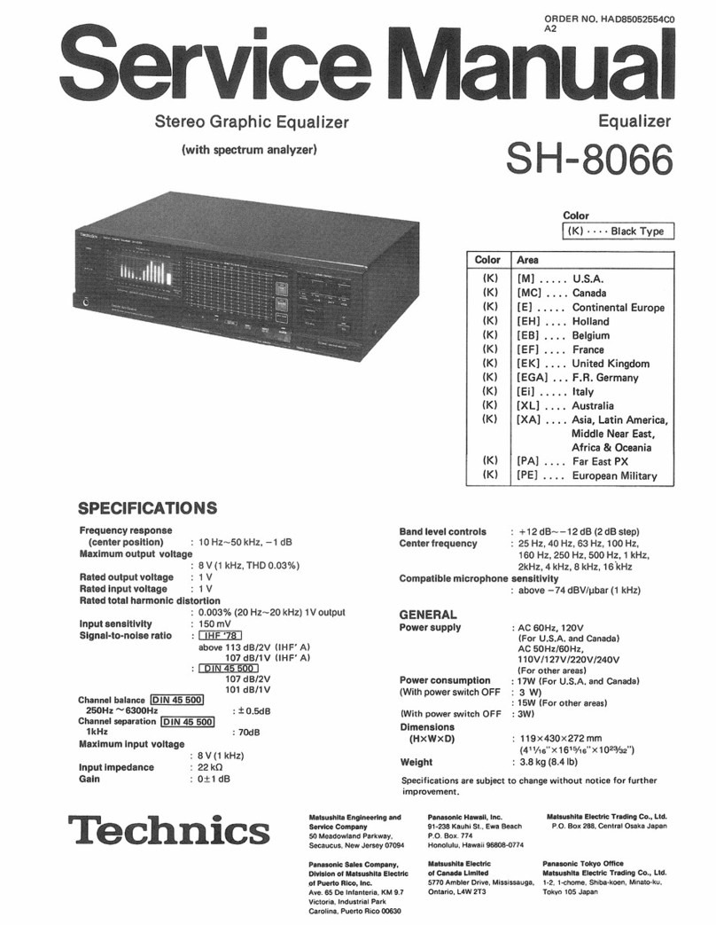
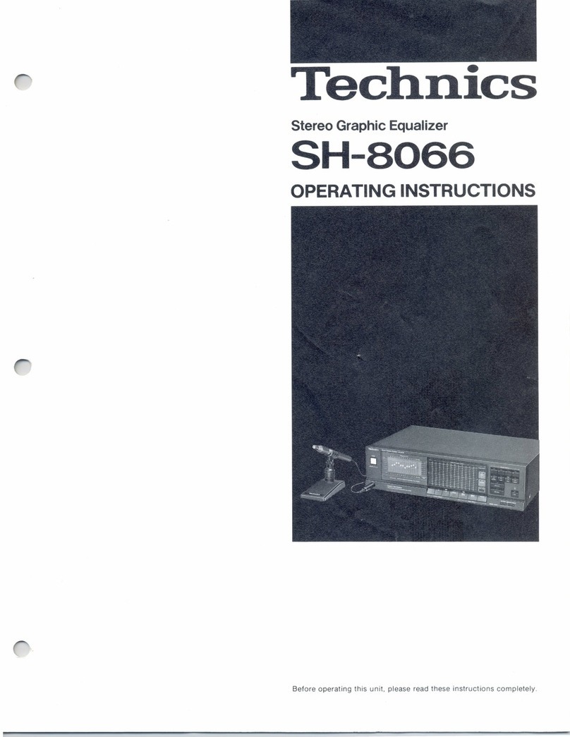
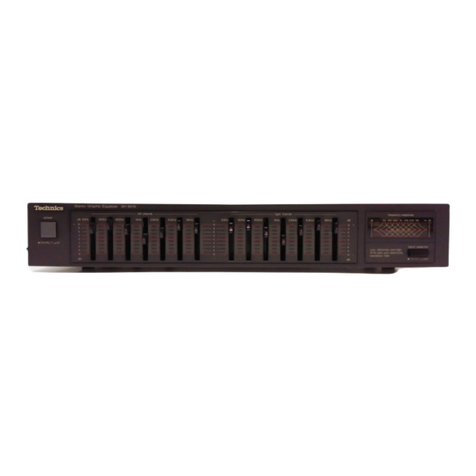
Technics SH-GE50 User manual

B
Specifications
@
Equalizer
Section
Frequency
response(center
position)
Viaximum
output
voltage
Rated
output
voltage
Rated
total
harmonic
distortion
nput
sensitivity
Signal
-to
-noise
ratio
Maximum
input
voltage
Input
impedence
Gain
Band
level
controls
5Hz~100kHZ,
-3dB
6V(1kHz)
1V
0.007%(20Hz~20kHz)
0.005%(1kHz)
1V
110dB(IHF'A)
6V
33
kQ
0+1
dB
+12dB
to
-12dB
(7
continuous
variable
elements
per
channel)
—
Contents
Page
CAUTIONS
FOR
AC
MAIN
LEADG.............:cccccccessseseeseeesseeeesseaees
2
OPERATION
CHECKS
iiiscsvecucicdeticavainccmdccavbrstaurcpintamanncentepeedeas
3~4
TERMINAL
GUIDE
OF
ICs
TRANSISTORS
AND
DIODES
........
5
SCHEMATIC
DIAGRAM.
...........cccccceessseseeeesensseeeesseesenesesaaeeensaaes
5~7
PRINTED
CIRCUIT
BOARD
..........c00cssscercssssssnssancsacssanccarssacseaeare
8~10
ORDER
NO.
MD9707075C2
Service
Manual
Stereo
Graphic
Equalizer
Equalizer
SH-GE50
=
:
ene
Black
Type
Area
Suffix
for
A
eB
W
(EG)
Germany
and
Italy
|
Center
frequency
63Hz,
160Hz,
400Hz,
1kHz
2.5kKHz,
6.3kKHz,
16kKHz
@
General
Power
supply
AC
230
-
240
V,
50
Hz
Power
consumption
11W
Dimensions
(W
x
H
x
D)
430
x
80.4
x
192.5
mm
|
(16°9/,."
X
3/55"
X
7'%/,5")
Weight
1.8kg
(3.95ib.)
Notes
:
1.
Specifications
are
subject
to
change
without
notice.
Weight
and
dimensions
are
approximate.
2.
Total
harmonic
distortion
is
measured
by
the
digital
spectrum
analyzer.
Page
WIRING
CONNECTION
DIAGRAM.
..........ccccececceeeneeeeeseeseesesenenenees
11
CABINETPARTS
LOCATION
Sickie
te
eee
12
REPLACEMENT
PARISLISDE
wisisstisuceseatcais
nsiiavnnuavianene
came
13
RESISTORS
&
CAPACITORS
xecicsustenceetietiscatenimcinics
14
4.
WARNING
This
service
information
is
designed
for
experienced
repair
technicians
only
and
is
not
designed
for
use
by
the
general
public.
It
does
not
contain
warnings
or
cautions
to
advise
non-technical
individuals
of
potential
dangers
in
attempting
to
service
a
product.
Products
powered
by
electricity
should
be
serviced
or
repaired
only
by
experienced
professional
technicians.
Any
attemptto
service
or
repair
the
product
or
products
dealt
with
in
this
service
information
by
anyone
else
could
result
in
serious
injury
or
death.
Technics’
©
1997
Matsushita
Electronics
(S)
Pte.
Ltd.
All
rights
reserved.
Unauthorized
copying
and
distribution
is
a
violation
of
law.
SH-GE50
|
—
Caution
for
AC
Main
Leads
(For
“EB”
area
code
model
only.)
|
For
your
safety,
please
read
the
following
text
carefully.
This
appliance
is
supplied
with
a
moulded
three
pin
mains
plug
for
your
safety
and
convenience.
A
5-ampere
fuse
is
fitted
in
this
plug.
|
Should
the
fuse
need
to
be
replaced
please
ensure
that
the
replacement
fuse
has
a
rating
of
5-ampere
and
that
itis
approved
by
ASTA
or
BSI
to
BS1362.
Check
for
the
ASTA
mark
@®
or
the
BSI
mark
CY
on
the
body
of
the
fuse.
If
the
plug
contains
a
removable
fuse
cover
you
must
ensure
that
it
is
refitted
when
the
fuse
is
replaced.
If
you
lose
the
fuse
cover,
the
plug
must
not
be
used
until
a
replacement
cover
is
obtained.
A
replacement
fuse
covercan
be
purchased
from
your
local
dealer.
CAUTION
!
IF
THE
FITTED
MOULDED
PLUG
IS
UNSUITABLE
FOR
THE
SOCKET
OUTLET
IN
YOUR
HOME
THEN
THE
FUSE
SHOULD
BE
REMOVED
AND
THE
PLUG
CUT
OFF
AND
DISPOSED
OFF
SAFELY.
THERE
IS
A
DANGER
OF
SEVERE
ELECTRICAL
SHOCK
IF
THE
CUT
OFF
PLUG
IS
INSERTED
INTO
ANY
13-AMPERE
SOCKET.
If
a
new
plug
ts
to
be
fitted,
please
observe
the
wiring
code
as
shown
below.
if
in
any
doubt
please
consult
a
qualified
electrician.
IMPORTANT
The
wires
in
this
mains
lead
are
coloured
in
accordance
with
the
following
code:
Blue:
Neutral
Brown:
Live
As
these
colours
may
not
correspond
with
the
coloured
markings
identifying
the
terminals
in
your
plug,
proceed
as
follows:
The
wire
which
is
coloured
Blue
must
be
connected
to
the
terminal
which
is
marked
with
the
letter
N
or
coloured
Black
or
Blue.
The
wire
whichis
coloured
Brown
mustbe
connected
to
the
terminal
which
is
marked
with
the
letter
L
or
coloured
Brown
or
Red.
WARNING:
DO
NOT
CONNECT
EITHER
WIRE
TO
THE
EARTH
TERMINAL
WHICH
IS
MARKED
WITH
THE
LETTER
E,
BY
THE
EARTH
SYMBOL
—
OR
COLOURED
GREEN
OR
GREEN/YELLOW.
THIS
PLUG
IS
NOT
WATERPROOF—KEEP
DRY.
Before
use
Remove
the
connector
cover.
How
to
replace
the
fuse
The
location
of
the
fuse
differ
according
to
the
type
of
AC
mains
plug
(figures
A
and
B).
Confirm
the
AC
mains
plug
fitted
and
follow
the
instructions
below,
Illustrations
may
differ
from
actual
AC
mains
plug.
1.
Open
the
fuse
cover
with
a
screwdriver.
Figure
A
Figure
B
2.
Replace
the
fuse
and
close
or
attach
the
fuse
cover.
Figure
A
Figure
B

SH-GE50
Mi
Operation
Checks
"ATTENTION
SERVICER"
Some
chassis
components
may
have
sharpe
edges.
Be
careful
when
disassembling
and
serving.
1.
This
section
describes
procedures
for
checking
the
operation
of
the
major
printed
circuit
boards
.
2.
For
reassembly
after
operation
checks
or
replacement,
reverse
the
respective
procedures.
Special
reassembly
procedures
are
described
only
when
required.
3.
Select
items
from
the
following
index
when
checks
or
replacement
are
required.
¢
Contents
¢
Checking
Procedure
for
Major
P.C.B.
Mi
Checking
Procedure
for
Major
P.C.B.
1.
Checking
of
the
Equalizer
P.C.B.
QOx3
Equalizer
P.C.B.
(Solder
Side)
&
}D
[sne2129-1)
(Black)
\b
)
[XTBS3+8JFZ1]
(Black)
2.
To
remove
the
front
panel
from
bottom
chassis
Front
Cabinet
Catch
Catch
Remove
the
top
cabinet.
Push
the
3
catch
and
pull
the
frontcabinet
simultaneously
in
the
direction
of
arrow.
‘Step
2)
Q«2

SH-GE50
3.
To
remove
Equalizer
P.C.B.
Remove
the
top
cabinet.
Step
2)
Gap
|
Remove
the
front
cabinet.
Oxi2
@
OO
o
9
Oo
Step
4
|
Remove
the
Equalizer
P.C.B.
in
the
direction
of
arrow
@
Equalizer
P.C.B.
one
c
]
[XTBS26+10J]
4.
Checking
of
Input
Selector
P.C.B.,
Meter
P.C.B.
and
Power
Switch
P.C.B.
‘Step
1]
Equalizer
P.C.B.
Input
Selector
P.C.B.
Follow
procedure
3
Power
Switch
P.C.B:
Meter
P.C.B.
(Solder
Side)
5.
Checking
of
Power
Supply
P.C.B.
and
In/Output
Terminal
P.C.B.
Exp
Cb
In/Output
Terminal
P.C.B.
Remove
the
top
cabinet.
Power
Supply
P.C.B.
(Imm
+O
[XTB3+20JFZ]
(Black)

Mi
Terminal
Guide
of
ICs,
Transistors
and
Diodes
M5229P
11
“Kg
i
25B621AQSTA
yA
PCs
SLR325MCT31
SLR325YCT31
Cathode”
Cao—tk}—0A
Anode
ai
*
M5218AP
SLR342VC
Anode
Cathode”
||
}{7”
Cao—{kp}—0A
mM
Schematic
Diagram
(All
schematic
diagrams
may
be
modified
at
any
time
with
the
development
of
new
technology)
Note
:
¢
S1
Power
switch
MLC4066BH
BAG144
MA2110BLF
Ca
‘il
Cathode
SLA370LT
SLA370MT
Cathode
i
Cac—tk}—oA
:
SH-GE50
RVTDTC143XST
25A933SSTA
23C1740SSTA
25D2374PQAU
B
Ce
MTZJ13BTA
RL1N4003NO02
Ca
Ca
Cathode
a
Cathode
A
a
A
Ea
Anode
°
$201
¢
VR201
&
VR202
¢
VR203
&
VR204
¢
VR205
&
VR206
Input
Selector
switch
Equaliser
control
(
63Hz
)
Equaliser
control
(1
60Hz
)
Equaliser
control
(
400HZ
)
¢
VR207
&
VR208
e
VR209
&
VR2010
¢
VR2011
&
VR2012
e
VR2013
&
VR2014
Equaliser
control
(
1kHz
)
Equaliser
control
(
2.5kKHz
)
Equaliser
control
(
6.3kHz
)
Equaliser
control
(
16kHz
)
¢
Signal
line
“ij
+
Playback
signal
line
AnC>
'
+Bline
:
Record
signal
line
:
-Bline
:
Main
signal
line
The
voltage
value
and
waveforms
are
the
reference
voltage
of
this
unit
measured
by
DC
electronic
voltmeter
(high
impedance)
and
oscilloscope
on
the
basis
of
chassis.
|
Accordingly,
there
may
arise
some
error
in
voltage
values
and
waveforms
depending
upon
the
internal
impedance
of
the
tester
or
the
measuring
unit,
elmportance
safety
notice:
Components
identified
by
A\
mark
have
special
characteristics
important
for
safety.
Furthermore,
special
parts
which
have
purposes
of
fire-
retardant
(resistors),
high-quality
sound
(capacitors),
low-noise
(resistors),
etc.
are
used.
When
replacing
any
of
components,
be
sure
to
use
only
manufacturer's
specified
parts
shown
in
the
parts
list.
Caution!
iC,
LSI
and
VLSI
are
sensitive
to
static
electricity.
Secondary
trouble
can
be
prevented
by
taking
care
during
repair.
«Cover
the
parts
boxes
made
of
plastics
with
aluminium
foil.
«Ground
the
soldering
iron.
«Do
not
touch
the
pins
of
IC,
LSI
or
VLSI
with
fingers
directly.
«Put
a
conductive
mat
on
the
work
table.

SH-GE50
mi
Schematic
Diagram
Meiners
[eer
4
Pt
|
—-
INPUT
SWITCH
CIRCUIT
elit
24
.
©
al
MIL
HO
Hey
e
L
CH
e
REC
(OUT
es
TAPE
(MONITOR)
rt
CHICO
iy
rial
R
CHO
(9)
MUTING
n
(>)
e118
Mw
NS
<OV>
o
£1
=
ae
af
MLC4066BH
|
|
SWITCHING(ON/OFF)
mg
IC2
M5218AP
BUFFER
AMP
0217-D222
0231-0234
LT
(L-T\
LT)
SLR325MCT31
SLA370LT
y,
SD
q
0223-0226
0235,0236
SLR325YCTS1
SLR342VC
{C203
,IC204
BA6144
LEO
INDICATOR
(2)
S
rome)
<10.8V>
<10.9V>
<10.9V>
<OV>
<OV>
A\R231
56
METER
CIRCUIT
rt)
(a
q

SH-GE50
CEE
FILTER
AMP/BAND
LEVEL
CONTROLS
CIRCUIT
C223,
|
KO.033
IDI)
rays
P=
OOP
C225
K680P
C226
K680P
C230
ov>
KSSOP
a
|
227
NH
=
K0.012
oF
2.EV>
>
<—2.1V>
~2.1V>
2.1V>
cree.
<OV>
<OV>
<OV
<
OV>
<OV>
<OV>
()
<12,.5V>
van
ah
oe
oe,
(1
Sem]
7m
Cm]
S|)
3)
2)
7)
ae)
Se
sas
|
|_|
ty
I
wy
(TS)
sta
ag
ey
yp
Na)
eae
|
Lee
|
epee
|
eee:
|
eerie!
|
Meera
|
Pree
ee
[Eger
|
Spree!
|
renee
|
Neeser)
|
LESeere
|
mse!
|
Eo
R202
2.2K
\
war
ragi,
16201
IC202
9229P
B.P.
FILTER
AMP
POWER/EQUALIZATION
SWITCH
CIRCUIT
mE
diim
_f
ft
She
ans
:
ae
3
SS
0201
ge
Sek
on
2SB621AQSTA
iS
=
iN
POWER
SUPPLY
ix
Q203
i 4
RVTDTC|
43XST
dws
eee
a
5
ae
Saas
Seca
a
ar
a
Pee
ie)
meen
aan
pee
aa
JW3A
sides
(aera
ET
A
>Peel
of
=
1601
“|
8]
F
8
eEEE
be
sine
REOS
Ee
<12.5V>-~<20.6V>
c
Ee
ge
ee
‘herr
|;
of
<13.1V)
iy
wo
©
|
|
:
A\YK601
()
|
|
x
Z50V-240
Zz
[|
4
D601
MTZJ13BTA
Dé02
MA24
10BLF
D603-D606
RLIN4G03N02
SShos74pqay
0603S
MAT
ABTA
MUTING
CONTROL
oO
(POWER
ON)
ex
$C
1740SSTA
7
ee
tow
Say
auins
ORE
EJ
POWER
CIRCUIT

SH-GE50
M@
Printed
Circuit
Board
Cc
B.P
FILTER
AMP/BMP
BAND
LEVEL
CONTROLS
P.C.B.
(REP2485C-M)
(16KHz)
(6.3KHz)
(2.5KHz)
(1KHz)
(400Hz)
(160Hz)
(63Hz)
RIGHT
=
CHANNEL
IE)
IN/OUTPUT
TERMINAL/BUFFER
AMP
P.C.B.
(REP2485C-M)
PLAY
(IN
REC
(OUT
OUT

SH-GE50
(16KHz)
(6.3KHz)
(2.5KHz)
(1KHz)
(400Hz)
(160Hz)
(63Hz)
LEFT
CHANNEL
[=]
POWER
P.C.B.
(REP2485C-M)
CAUTION
RISK
OF
ELECTRIC
SHOCK
AC
voltage
line.
Please
do
not
touch
this
portion.
AC
IN~
Z250V—240V
SO0Hz

SH-GE50
[]
POWER/EQUALIZATION
[3
INPUT
SWITCH
P.C.B.
SWITCH
P.C.B.
(REP2485C-M)
(REP2485C-M)
=
4022

|
SH-GE50
Mi
Wiring
Connection
Diagram
JWS5
JWa4
COMPONENT
SIDE
JW5A
T601
TRANSFORMER
[py
POWER/EQUALIZATION
SWITCH
P.C.B.
[EJ
POWER
P.C.B.
COMPONENT
SIDE
ore
a
[Sl
INPUT
SWITCH
P.C.B.
METER
P.C.B.
B.P
FILTER
AMP/BMP
BAND
LEVEL
CONTROLS
P.C.B.
COMPONENT
SIDE
COMPONENT
SIDE
(EQ)
Low
[J
REG
i)
TAPE
PLAY
(IN)
COMPONENT
SIDE
COMPONENT
SIDE
Ey
IN/OUTPUT
TERMINAL/BUFFER
|
AMP
P.C.B.
JW1
Saw
iE
[eee

SH-GE50
M@
Cabinet
Parts
Location
N/OUTPUT/BUFFER
TERMINAL
.C.B)
Nuwe
q
(B.P
FILTRER
AMP/BMP
BAND
LEVEL
CONTROLS
P.C.B)
OWER/EQUALIZATION
2)
SWITCH
P.C.B)
JW6A
(INPUT
SWITCH
P.C.B)
St
mee

Mi
Replacement
Parts
List
Notes:
*
Important
safety
notice:
Components
identified
by
A\
mark
have
special
characteristics
important
for
safety.
|
SH-GE50
Furthermore,
special
parts
which
have
purposes
of
fire-retardant
(resistors),
high-quality
sound
(capacitors),
low-noise
(resistors),
etc.
are
used.
When
replacing
any
of
components,
be
sure
to
use
only
manufacturer's
specified
parts
shown
in
the
parts
list.
*
[M]
in
Remarks
column
indicates
parts
that
are
supplied
by
MESA.
RefNo
Part
No.
Part
Name
&
Description
|
Remarks
|
[Ref
No
Part
No.
Part
Name
&
Description
}
Remarks
CABINET
AND
CHASSIS
|
RFKGHGESOEK
|FRONT
PANEL
ASS’Y
SGPK420-7B
|BOTTOM
CHASSIS
SGPK420-70
|BOTTOM
CHASSIS
SKCK200K99
|
TOP
CABINET
RKQ0089
-
|PCB
HOLDER
LEG
LEG
CUSHION
|
17
218
D219
[M
[MIE
SLR325MCT31
SLR3825MCT31
SLR325MCT31
oe
= E =
=
@>
mi
Oo
nh
220
D221
D222
SLR325MCT31
SLR325MCT31
{
K
D223
|
SLR325YCT31
D224
D225
D226
231
ola]!
w
ol
w
wo
(S15
515
5D
wi
at
w
qo
|
g&
(eh)
wa
Pw
>
™
nh
|
ho
ro
eil¢eiec
oe
2
=
2
O1o
3
ala
=
ee
wo
Rquoase-K
[POWER
VCR2
BUTTON
LIGHT
GUIDE
LED
SHEET
VOLUME
KNOB
LIGHT
GUIDE
BLIND
SHEET
SCREW
SCREW
(FOOT)
SCREW
(FRONT)
SCREW
SCREW
(CABINET)
BUTTON
K
SLR325YCT31
m
,
©
Bg
G)
mi
1
RKWO0509-K
og
a1o
=|z
=|/2)8)\¢
5
|=
rs
21s
BIS
Oo]
3 |
>
rm
.
D234
D235
wo
ia
=
o
ow
w
Na
+
o
a&>
w
ra)
SLAS70OLT
SLR342VC
SLR342VC
MAT65TA
MTZJ13BTA
MA2110BLF
RLIN4003N02
RLIN4003N02
RLIN4003N02
D606
|
RLIN4003N02
D607
|
MAI65TA
D608
|
MAI65TA
D609
|
MAI65TA
MAI65TA
MA165TA
4
RMF0248
XTB3+20JFZ
—i
on
D237
D601
ea
|
XTBS26+10J
XTBS3+8JFZ1
SNE2129-1
o
—_—
=
—
—
‘
‘
‘
&
9
D603
D604
INTEGRATED
CIRCUITS
IC,
EQ
IC,
BUFFER
AMP
IC,
FILTER
IC,
FILTER
IC,
MASTER
IC,
MASTER
oe
C2
C201
C202
C203
MLC4066BH
M5218AP
M5229P
BAG144
BA6144
—
D611
z
zlz|z
>
|B
|
C204
VARIABLERESISTORS
EWANWOJ15G15
|
VARIABLE
RESISTOR
EWANWO0J15G15
}
VARIABLE
RESISTOR
EWANWO0J15G15
|
VARIABLE
RESISTOR
EWANW0J15G15
EWANWOJ15G15
TRANSISTORS
fai
|
2sD1ei5FTA
|
TRANSISTOR
a
ass
eres
eaeren
}aeot
|
2s02974PQAU
ii
re
VR201
VR202
VR203
VR204
VR205
VR206
VR207
VR208
VARIABLE
RESISTOR
VARIABLE
RESISTOR
EWANW0J15G15
|
VARIABLE
RESISTOR
EWANW0J15G15
|
VARIABLE
RESISTOR
EWANW0J15G15
|
VARIABLE
RESISTOR
EWANWO0J15G15
|
VARIABLE
RESISTOR
VR209
oes,
fc
Ref
No
Remarks
Part
Name
&
Description
EWANWOJ15G15
|VARIABLE
RESISTOR
EWANWOU15G15
EWANWOJ15G15
|VARIABLE
RESISTOR
EWANWOUI5G15
EWANWOJ15G15
|VARIABLE
RESISTOR
Le
ee
SWITCHES
SW.
INPUT
SELECTOR
od
COILS
&
TRANSFORMERS
RTP1U4E001-V
|TRANSFORMER
VR210
211
VR212
13
VR214
ypiw
m7
m
alan
=
=
ua
iv
>
>
ro
|
rn
z=
=
o;o
=
=
3/2
o
RS
|
om
S
ad
on
an
7
3)
2
an
an
<—
=
=
ay
wv
>
>
oo
ow
rT
rT
m
m
ms
aw
m
m
O
ee
ot
3
oO
oO
a
wm
601
—+
LBL
EPPEL
ERPPETE
EARTH
TERMINAL
{
EARTH
TERMINAL
;
[M]
JACKS
JK,
LINE
IN
JK,
LINE
IN
JK,
AC
INLET
Ki
JF3069N
K2
K601
—
m
—
ow
<=
<=
med
8
wn
w
=
m
—_h,
So
©
>
nM
(a
16>)
JF3069N
w
JS9236-1
PACKING
MATERIALS
PACKING
CASE
PACKING
CASE
PACKING
CASE
MIRAMAT
BAG
POLYFOAM
(L)
POLYFOAM
(R)
1
—
1
2
3
P4
SPSK121-1
PSK122-2
®
E>
1
{
2
3
3
3
24
|AC
CORD
AC
CORD
|
STEREO
CABLE
INSTL
MANUAL
ASS'Y
INSTL
MANUAL
ASS’Y
OA
BOOK
[
=
m
G>
m
>
a
au
(fp)
wm
a
ms
au
cj
Oo
ee
i
Oe
i
On
|
aE
2/8/8183
Sif
alsa
l
Zig
®@
|
©
“18/8
]8
{
dae
RJL2P004B08
RFKSHGESOEBK
RFKSHGES0EK
RQT3904-B
[MJE
®
=
m
uw

SH-GE50
|
M@
Resistors
&
Capacitors
Notes
:*
Important
safety
notice:
Components
identified
py
A\
mark
have
special
characteristics
important
for
safety.
Furthermore,
special
parts
which
have
purposes
of
fire-retardant
(resistors),
high-quality
sound
(capacitors),
low-noise
(resistors),etc.
are
used.
When
replacing
any
of
components,
be
sure
to
use
only
manufacturer's
specified
parts
shown
in
the
parts
list.
*
Capacitor
values
are
in
microfarad
(uF)
unless
specified
otherwise,
P=Pico-farads
(pF)
F=Farads
(F)
*
Resistors
values
are
in
ohms,
unless
specified
otherwise,
1k=1,000(OHM),
1M=1,000k(OHM)
Values
&
Remar
ef
No.
Values
&
Remarks
ERDS2TJ681T
1/4W
[M]
|
/C207
|
ECEAIHKAQIOB
}
1
50V[M]
1
680
M
ERDS2TJ68iT
|680
1/4W
[M]||C208
|
ECEA1HKAO10B
50V.
[M
ERDSIFVJ560T
A\
156
1/2W
[M]
|
{C209
M
[
[
ECFRIE333KR
ERDS2TUA73T
{
|
[
Values
&
Remarks]
|Ref
No
RESISTORS
Fel
ERDS2TJ104T
ERDS2TJI04T
231
ERDS2TJ222T
232
ERDSZTJ222T
—
[2.2K
1/4W
[M}
|
[R293
ERDS2TJ3327
236
ef
No
Part
No.
Values
&
Remarks
B
Ref
No
Part
No.
Part
No.
Part
No.
Pe
—all
1
et
ime
‘?)
ry)
210
|ECFRIES33KR
0.033
25V
[M
ERDS2TJ472T
4.7K
1/4W
[M]
|}C211
|
ECEA1HKAR47B
[0.47
50V
ERDS2TU333T
33K
1/4W
[MI
M}
212
|
ECEAIHKAR47B
ERDS2TJ101T
213
|
ECFRIE123KR
ERDS2TJ471T
[470
1/4W
[M]
||C214_
|
ECFRIE123KR
ERD2FCVG100T
215
|
ECEAIHKAR22B
ERG2ANIP221HA\|
220
2W
[M]
||c216
|
ECEATHKARZOB
ERDS2TU562T
217
|
ECBTIC392KR5
ERDS2TJ222T
218
|
ECBTIC392KR5
ERDS2TU472T
147K
1/4W
(M}{|C219
|
ECQVIH683UM3
|
0.068
SOV
[M
ERDS2TU473T
«|
47K
~—-1/4W
[M}
||c220
|
EcaviHessuMa
609
|
ERDS2TJ273T
201
|
ECBT1C182KR5
610
|
ERDS2TU103T
209
|
ECBTIC182KR5
611
|
ERDS2TJ224T
223
|
ECFRIE333KR
a
ne
ECBT1H101KBS
224
|ECFRIES33KR
|
0.033
25V_
[MI
ECBTIHI01KB5
|100P
50V
[M|
Bi
2)
ERDS2TJ332T
601
ERDS2TJ102T
602
ERDS2TJ102T
603
ERDS2TJ102T
604
ERDS2TJ102T
605
11
|
ERDS2TUIO4T
2
|
ERDS2TJ104T
13
|
ERDS2TJ473T
14
|
ERDS2Tu473T
ERDS2TJ104T
16
|
ERDS2TI104T
17
|ERDS2TIO3T
«10K
=
1/4W
[M
18
|
ERDS2TJ103T
19
|
ERDS2TUI04T
ERDS2TJ104T
|
100K
1/4W
[MI]
ERDS2TJ222T
ERDS2TJ222T
ERDS2TJ2727
ERDS2TJ272T
680
1/4W
[MI
a
oO
7
pane
<i
home
beri
—
oot
Larner
—
10
i?)
606
607
608
weet
pare
©
oe
wa
Oo
wv
hell
a
ms)
pa
8
xa
1
2
3
4
evel
201
202
—e
mm
ism
oT
Oo
P|
e
212
S|
S
3/3
am]
oo
>)
5
6
203
oO
oO
J
m
m
mM
m
fTt
mr
m
m
m7
O1Ololalolalaliolo
oo
co
“Tt
'?)
oO
m
m m
m
aA/3/alal/Dl]rl
rl]
>]
>
—
—
—
=e
=a
—
wt
—
—_—
Pe
|
eee
eS)
ee
—
pew
SI8i8/elcol|>
S|f1s
— _
-.%
+.
>
—
a
a
Oe
|
ota
lFP
Vr
PapTaya
yaya
w
ao
tau)
w
211
213
214
215
R216
217
m
‘?)
oe)
>
oo
ba
|
=
5
="
=
oO
oO
=
=]
~*~
io
wm
cn
8
9
10
11
12
243
244
601
205
|ECBTIH68iKB5
|680P
SOV
[M]
296
|
ECBT1H681KB5
207
|
ECFRIE123KR
ECBTIHI01KB5
208
|
ECFRIE123KR
ECBT1H101KBS
209
|
ECBT1H331KB5
ECBT1H101KB5
200
JecBTinasiKes
|
930P Sov.
[M]|
235
|
ECEAQJKA3310
ECBTIH101KB5
24
ECBT1H101KBS
249
47
28V
[Mj
602
mimi
mi
wim
im]
mm]
mi
im
ee
eae
eed fee
em
ee
a
SIZ/S/ESE;A/S/E1e
TMIZ/SI1QiQ]
mela]
m
SIS
|SIElE
sia\el=
nmI171/9P;7
or
rsaimia};z2]
a
on
oloalV’i/n”igia
m
m
m
m
mm
Mm
Mm
m
m
UiwDWjindy
voaDiwvayi
i
vpinaiwv)]
wv
BIBIBIEI
BIBI
elle
ph
N
law
Nh
BD
nh
ho
nh
RO
ajoitierafeadtaidia
a
o>
>
cep)
co
ce
Cc
co
a
oo
co
&
oo
nN
nm nr
Le]
ao
chs
ed sy
—_,
_*
oh,
ae
—h
a,
Al/Al/a7a4
fa
/ayayayra
219
680
1/4W
[M]
|
IC14
604
A101
680
1/4W
[M]
|
{C15
C605
EADs2TsseiT
|
560
1/4W
[M]
JICt6
222
|
ERDS:
C17
0.01
25v
[Mi
||ceo7
|
608
609
610
611
m
2)
Fax)
J
rh
=
o>
oO
nh
ma)
m
201
202
203
204
|
205
206
223
|
0
es
—
Printed
in
Singapore
—14—
MESA
G9707
08000
P/S/T/J
era
[88
sO
verano
[oo
sv
0.068
50V
[Mj
4.7K
1/4
[M]
mimimimtiolio
S/S/S/8/8/8
</2/2/2/3/3
zr
zilaxrixJiJ=
SISl|AIAIS|S
co
|
o
>i
awit
2g
6
fe
Wa
(ee
=ill1Gtiw
i]
@
iw
ora
il
oliloyT~
rin
Tw
imi
m
He
>|]
=
celml=
~
>
EIS
|e
Sly]
oa
wala
227
mimiemnmimimimim
iy.
Divi
vivnivdiwnaiw
QiIol;lror;l;o;1o;holso
Oirinili
ini
ni
ini
nas!
ow
SISISi8(818/8
ja
peoq~ajerpognungpfjuoeitn
mm
F
B&B
|
PO
FR
Ft
—s
=
ft
tn
sisjiyiys{als
|
2
aAhatfatayafpyaqya
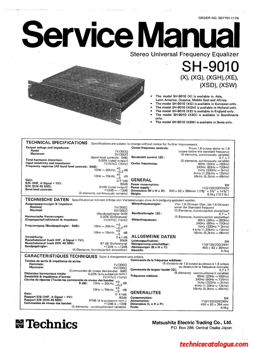
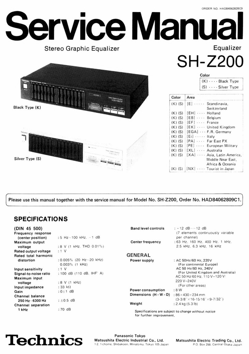
Other Technics Stereo Equalizer manuals

Technics
Technics SH-Z200 User manual

Technics
Technics SH-8016 User manual

Technics
Technics SH-GE70 User manual

Technics
Technics SH-8066 User manual

Technics
Technics SH-8066 User manual

Technics
Technics SH-9010 User manual

Technics
Technics SH-8075 User manual

Technics
Technics SH-9010 User manual

Technics
Technics SH-8038 User manual

Technics
Technics SH-8066 User manual