manuals.online logo
Brands
  1. Home
  2. •
  3. Brands
  4. •
  5. Technics
  6. •
  7. Stereo Receiver
  8. •
  9. Technics SA-203 User manual

Technics SA-203 User manual

ORDER
NO.
SD82082280C2
ervice
Manual
FM/AM
Stereo
Receiver
SA-203
[EGA]
SA-203(K)
[EGA]
*
The
cabinet
and
front
panel
are
available
in
black
color
and
silver
Area
types.
*
The
black
type
model
is
provided
with
(K)
in
the
Service
Manual.
*
[EGA]
is
available
in
F.R.
Germany.
TECH
N
]
SCH
E
DATE
N
(Spezifikationen
K6nnen
infolge
von
Verbesserungen
ohne
Ankiindigung
geandert
werden.)
(DIN
45
500)
@
VERSTARKERTEIL
Gerauschabstand
Nennleistung
(4
©)
Phono
Aux,
Tape
—26
dB
Leistung
(4
Q)
Phono
Aux,
Tape
50
mW
Leistung
(4
©)
Phono
Aux,
Tape
Frequenzgang
Phono
70
dB
(nach
IHF,
A:
78
dB)
Dauerton-Ausgangsleistung
bei
20
Hz
~
20
kHz
88
dB
(nach
IHF,
A:
95
dB)
beide
Kandle
ausgesteuert
2
X
30W
(4.9)
2
X
30W
(8
Q)
Dauerton-Ausgangsleistung
bei
40
Hz
~
16
kHz
beide
Kanile
ausgesteuert
2X:
30W
(4
Q)
2
X
30W
(8
)
64
dB
66
dB
62
dB
Dauerton-Ausgangsleistung
bei
1
kHz
62
dB
beide
Kanadle
ausgesteuert
2
X
35W
(4
Q)
2
X
33W
(8
Q)
RIAA-Standardkurve
+0,8
dB
(30
Hz
~
15
kHz)
5
Hz
~
70
kHz2(
-3
dB)
+0,2
dB
(20
Hz
~
20
kHz)
GehGrrichtige
Lautstarkekorrektur
(Loudness)
(bei
-30
dB
Ausgangsleistung)
Ausgangsspannung
und
-impedanz
Tape
Aufnahme
(TAPE
REC
OUT)
Gesamtklirrfaktor
Nennleistung
bei
20
Hz
~
20
kHz
0,08%
(4
Q)
0,04%
(8
Q)
0,08%
(4
Q)
0,04%
(8
Q)
0,04%
(4
9)
0,04%
(8
Q)
0,025%
(8
Q)
Aux,
Tape
Nennleistung
bei
40
Hz
~
16
kHz
Nennleistung
bei
1
kHz
50
Hz,
+9 dB
150
mV
halbe
Nennleistung
bei
20
Hz
~
20
kHz
halbe
Nennleistung
bei
1
kHz
—26
dB
Leistung
bei
1
kHz
50
mW
Leistung
bei
1
kHz
Intermodulationsfaktor
Nennleistung
bei
250
Hz:
8
kHz
=
4:1,
4
Q
0,08%
Nennleistung
bei
60
Hz:
7
kHz
=
4:1,
nach
SMPTE,
8
Q
0,04%
0,009%
(8
1)
0,1%
(4
9)
0,12%
(4
Q)
Leistungsbandbreite
beide
Kandle
ausgesteuert
bei
—3
dB
10
Hz
~
30
kHz
(4
)
Dampfungsfaktor
15
(4.Q),
30
(8.Q)
Eingangsempfindlichkeit
und
-impedanz
Phono
2,5
mV/47
kQ
Aux
150
mV/22
kQ
Tape
180
mV/22
kQ
Maximale
TA-Eingangsspannung
(1
kHz,
eff.)
130
mV
Klangregler
Bafregler
(BASS)
Hdhenregler
(TREBLE)
‘Technics
50
Hz,
+10
dB
~
—10
dB
20
kHz,
+10
dB
~
-10
dB
+1
dB
55
dB
260
mV/330
Q
Kanalabweichung
(Aux,
250
Hz
~
6300
Hz)
Obersprechdaémpfung
(Aux,
1
kHz)
KopfhGrerpegel
und
-impedanz
Lautsprecherimpedanz
MAIN
oder
REMOTE
MAIN
und
REMOTE
4Q~169
8Q~
169
@
UKW-TUNERTEIL
Wellenbereich
87,5
~
108
MHz
Eingangsempfindlichkeit
S/R
30
dB
S/R
26
dB
S/R
20
dB
Nutzempfindlichkeit
nach
IHF
Gesamtklirrfaktor
Mono
:
:
0,15%
Stereo
0,2%
1,3
pV
(75.9)
1,2
pV
(75
Q)
0,9
pV
(75
Q)
1,5
pV
(nach
IHF
’58)
Matsushita
Electric
Trading
Co.,
Ltd.
P.O.
Box
288,
Central
Osaka
Japan
Gerduschabstand
@
MW-TUNERTEIL
Mono
60
dB
(75
dB
nach
IHF)
chads
58
dB
(70
dB
nach
IHF)
Welllenbereiche
525
~
1605
kHz
Frequenzgang
20
Hz
~
15
kHz(+1dB~-2dB)
—_
Bingangsempfindlichkeit
(S/R
20
dB)
30
pV,
300
yV/m
Trennscharfe
bei
Stérsender
75
dB
Trennscharfe
30
dB
Einfangverhaltnis
1,2
dB
Spiegelfrequenz-Dampfung
bei
1000
kHz
50
dB
Spiegelfrequenz-Dampfung
bei
98
MHz
55
dB
ZF-Dampfung
bei
1000
kHz
40
dB
ZF-Dampfung
bei
98
MHz
75
dB
Ansprechdampfung
auf
Nebenfrequenzen
bei
98
MHz
80
dB
MW-Unterdriickung
50
dB
Obersprechdémpfung
1
kHz
40
dB
10
kHz
30
dB
19
kHz
~30
dB
(-35
dB
nach
IHF)
Netzspannung
38
kHz
—50
dB
(—50
dB
nach
IHF)
Wechselstrom
50
Hz/60
Hz,
220V
Kanalabweichung
(250
Hz
~
6300
Hz)
+1,5
dB
Abmessungen
(BXHXT)
430
X
86
X
320
mm
@
ALLGEMEINE
DATEN
Leistungsaufnahme
300
W
Tragerrest
Begrenzereinsatz
1,2
uV
Gewicht
6,6
kg
Bandbreite
ZF-Verstarker
180
kHz
UKW-Demodulator
1000
kHz
AntennenanschluB
75
Q
(unsymmetrisch)
Hi
CONTENTS
Page
Page
LOCATION
OF
CONTROLS
.......
00. ewe
nt
eens
2,3
CIRCUIT
BOARD
AND
WIRING
CONNECTION
TECHNICAL
GUIDE
........
2.2
ce
ec
eee
eee
4
DIAGRAM
.....
2.0.2
ee
ee
eee
et
we
we
13
~16
DISASSEMBLY
INSTRUCTIONS
............85%
5~7
SCHEMATIC
DIAGRAM...........20
000
ee ae
17
~21
MESSUNGEN
UND
JUSTIERUNGEN
........005
8~10
REPLACEMENT
PARTS
LIST
(Electrical
Parts)......
22
~24
DIAL
CORD
INSTALLATION
GUIDE
.........00065
10
EXPLODED
VIEW
......
0-2
ee
een
eee
en
ena
24,
25
BLOCK
DIAGRAM
.....
2...
0c
cee
erent
ees
11,12
REPLACEMENT
PARTS
LIST
(Cabinet
and
Chassis
Parts)
.
.
26
Mi
LOCATION
OF
CONTROLS
Peak-power
indicators
Tuning
indicator
{W/pointer)
Power
display-range
selector
Tape-monitor
selector
(
J
source,
=
tape)
(off
«>»
x1
+»
x0.01)
FM
stereo
indicator
Power
Signal-strength
indicators
Headphones
jack
FM
phono
|
AM
Speaker
men)
aux
selectors
(remote)
Input
selector
Tuning
Volume
control
FM
muting/FM
mode
selector
(
Hl
on/FM
auto,
=
off/FM
mono)
Loudness
(
M
off,
=
on)
(Ground)
AM
antenna
terminal
AM
ferrite-bar
antenna
coil
Main
speaker
terminals
FM
antenna
terminal
(75Q.
coaxial)
Ground
Phono
input
Aux
input
(rec
out)
el
(playback)
Remote
speaker
terminals
*
Phono
input
capacitance
is
about
150pF.
FM
IF
amp.
&
FM
detector
circuit
FM
MPX
circuit
Tuning
gang
Power
amp.
circuit
Power
transformer
circuit
Power
supply
circuit
Equalizer
circuit
Differential
amp.
circuit
_SA-203
|
M@
TECHNICAL
GUIDE
The
power
amplifier
!C
(SV!STK2028)
is
provided
with
a
protection
circuit.
1.
Muting
(shock
noise
prevention)
with
power
switch
ON.
(1)
When
power
is
supplied,
negative
voltage
is
applied
to
the
emitter
of
switching
transistor
(Q703).
(2)
Positive
voltage
flows
from
the
regulator
(Q707)
to
R709
and
R708
to
turn
D705
and
Q703
ON.
(It
takes
a
few
seconds
until
0703
turns
ON
due
to
time
constant
of
C706).
(3)
When
Q703
turns
ON,
negative
voltage
is
applied
to
the
pin
©)
of
input
amplifier
1C
(AN7O60)
causing
the
input
amplifier
to
operate.
*
The
signal
is
applied
to
the
power
amplifier
a
few
seconds
later
so
that
shock
noise
can
be
prevented.
2.
Muting
(shock
noise
prevention)
with
power
switch
OF
F.
(1)
When
power
supply
is
cut
off,
the
voltage
applied
to
Q703
drops
at
the
base
faster
than
the
negative
voltage
at
the
emitter
connected
to
the
large
capacity
condenser,
thus
turning
off
D705
and
Q703.
(2)
Input
amplifier
is
off
with
708
off.
*
The
signal
is
cut
off
on
the
input
side
while
the
operation
voltage
of
power
amplifier
still
remains,
thus
preventing
shock
noise.
3.
Operation
of
the
protection
circuit
with
speaker
terminal
short-circuited.
(1)
Transistor
Q7
in
the
power
amplifier
|C
(SViISTK2028)
is
usually
OFF,
but
when
the
speaker
terminal
is
short-circuit-
ed
to
the
ground,
a
large
amount
of
current
flows
to
Q6,
causing
a
voltage
to
be
generated
at
R5.
(2)
The
voltage
causes
Q7
to
turn
ON,
then
(Ii)
flows
to
raise
the
base
potential
of
702.
And
Q702
turns
ON.
(3)
As
Q702
is
ON,
®
flows
to
generate
a
voltage
at
R707,
and
then
0701
turns
ON.
(4)
G)
flows
with
Q701
turned
ON,
®
flows
to
hold
Q702
ON.
(5)
The
current
flowing
in
R709
increases
due
to
),
and
the
positive
voltage
from
regulator
(0707)
drops,
causing
D705
to
turn
off.
(6)
tn
other
words,
Q703
turns
OFF
and
the
negative
power
supply
to
the
input
amplifier
is
discontinued.
*
This
condition
continues
until
power
supply
switch
is
set
OFF.
A
few
minutes
after
the
power
switch
is
set
to
ON,
if
no
sound
is
produced
while
the
operation
is
normal,
cut
off
the
power
supply
and
check
the
speaker
connections
and
the
input
equipment.
(C601
©.
{C603
(SVISTK2028)
Power
Amp.
1C601,
602
AN7060
Differential
Amp.
1C602
Ck
a
eS.
ZO:
(}
oe
Se
oe
oS
ee
eee
Ive
ee
Nel
|
ERE
From
regulator
(0707)
Ov
Mi
DISASSEMBLY
INSTRUCTIONS
1.
—
@
ao
BW
DN
How
to
remove
the
cabinet
Remove
the
5
setscrews
(Fig.
1:
@~
@)
of
the
cabinet.
.
Remove
the
cabinet.
How
to
remove
the
front
panel
.
Remove
the
cabinet.
(Refer
to
the
section
“How
to
remove
the
cabinet.”
}
.
Remove
the
4
setscrews
(Fig.
1:
@,
@
and
Fig.
2:
@,
©)
of
the
front
panel.
.
Remove
the
1
setscrew
(Fig.
1:
@)
of
the
transparent
plate
bracket,
then
remove
the
front
panel.
How
to
remove
the
dial
scale
.
Remove
the
cabinet.
(Refer
to
the
section
‘‘How
to
remove
the
cabinet.’’)
.
Remove
the
front
panel.
(Refer
to
the
section
‘“How
to
remove
the
front
panel.’’)
.
Pull
up
the
two
claws
at
the
bottom
of
the
transparent
plate
in
the
direction
of
the
arrow
8]
(Fig.
3).
.
Remove
the
dial
indicator
lamp
and
the
2
dial
scale
holder
of
the
front
chassis.
(see
Fig.
4)
.
Remove
the
dial
scale.
How
to
remove
the
peak-power
indicators
printed
circuit
board
.
Remove
the
cabinet.
(Refer
to
the
section
‘How
to
remove
the
cabinet.)
.
Remove
the
front
panel.
(Refer
to
the
section
“How
to
remove
the
front
panel.’’)
.
Remove
the
power
display/range
knob
(Fig.
3).
.
Remove
the
2
setscrews
(Fig.3:
@,
@)
of
the
front
chassis.
.
Remove
the
2
lugs
(Fig.
4:
@,
@)
to
detach
the
peak-power
indicators
printed
circuit
board.
Front_
Cabinet
.
2]
a)
panel
[Fig.
1]
Front
panel
[Fig.
2]
Dial
scale
P))
holder
|
Dial
scale
holder
(Rubber)
NI
Dial
scale
Pare
SS
SX
Peak-power
indicators
SK
SS
printed
circuit
board
[Fig.
4]
Power
amplifier
IC
Rear
panel
Front
panel
[Fig.
7]
jterminal
late
(rare
et
AM
antenna
coil
Rear
panel
Speaker
terminal
case
c—
fae
|
a
3
0000/0l0004
Input
terminals
Antenna
terminals
Speaker
terminals
AC
cord
Oo
©
O©D0®
2@
Go
[Fig.
5]
AM
antenna
coil
Rear
panel
=
|
Sodd
©
[6060
:
@
20
s2/0lop0Fle
ooo
|
Input
terminals
Antenna
terminals
Speaker
terminals
AC
cord
[Fig.
6]
e
How
to
remove
the
power
amplifier
IC
1.
Remove
the
cabinet.
(Refer
to
the
section
“How
to
remove
the
cabinet.’’}
2.
Remove
the
6
setscrews
(Fig.
2:@,@and
®@~
@)
and
3
setscrews
(Fig.
5:
@
~
@
)
of
the
speaker
terminal
case.
3.
Remove
the
speaker
terminal
case.
4.
Remove
the
2
setscrews
(Fig.
6:
@
,
@
)
of
the
heat-sink.
5.
Remove
the
3
setscrews
(Fig.
7:
@
~
®).
6.
Pressing
the
claws
of
the
input
termina!
plate
and
antenna
terminal
plate
in
the
direction
of
arrow@
(Fig.
7),
lift
up
the
front
panel
in
the
direction
of
arrow
@
(Fig.
8).
Then,
the
front
panel
can
be
removed
from
the
rear
panel.
7.
Remove
the
2
setscrews
(Fig.9:
@
,@
)
of
the
heat-sink,.
8.
Unsolder
the
power
amplifier
!C.
(Fig.
9).
9.
Remove
the
2
setscrews
(Fig.
10:
@
,
@
)
used
to
secure
the
power
amplifier
IC
on
the
heat-sink,
and
then
pull
the
power
amplifier
IC.
10.
When
mounting
the
power
amplifier
IC,
apply
silicone
compotnd
(or
equivalent
heat
diffuser)
to
the
back
of
power
amplifier
IC.
Note
1:
Note
2:
[Fig.
8]
Heat-sink
Bottom
view
[Fig.
9]
When
checking
or
repairing,
remove
the
speaker
from
the
speaker
terminal.
If
it
is
necessary
to
check
or
repair
without
removing
the
speaker
from
the
terminal,
short-circuit
the
phono
input
terminal
beforehand.
Setscrew
@
(Fig.
6)
is
screw
with
detents
(Part
No.:
XTBS3+8BFZ)
as
shown
in
Fig.
11-A
in
order
to
make
the
contact
of
electric
circuit
perfect.
Take
care
not
to
mix
up
these
screws
with
other
screws.
When
substituting,
use
a
3
x
8mm
tapping
screw
(Part
No.:
XTB3+8BFZ)
and
toothed
lock
washer
(Part
No.:
XWC3B)
as
shown
in
Fig.
11-B.
The
teeth
of
the
lock
washer
should
be
positioned
on
the
chassis
side.
Rear
panel
Heat-sink
Power
amplifier
IC
[Fig.
10]
Detent
XTBS3+8BFZ1
Detent
Ot
pip
)--*783+88F2
VA
AVY
3
Detent
[Fig.
11]
Mi
MESSUNGEN
UND
JUSTIERUNGEN
Pull
out
AM
ANT
FM
MPX
FM
DET
Trimmer
FM
Discri
{FT
©@RGRE
5
ofr
set
FS
AM
ANT
Trimmer
©
(L302L301)
(L303)
fl
FM
ANT
I
Trimmer
]
a
CTI
AM
OSC
Trimmer
FM
OSC
Trimmer
FM
Muting
Level
Adj.
AM
IFT
FM
IFT
(2nd)
GS
SS
css
q
Input
—»
->
Output
'
37.560
;
From
FM-SG
7
750
|
To
antenna
(759)
!
!
terminal(759)
DC
VOLTMETER
Ceres
es
=
[Fig.
12]
(Abb.
12)
wale
7
Noise
A
COIL
[100pH)
Se
(SLOX101—20)
F
zs,
§
@
©
@®
©
‘
VR301
e101)
Te1Oe
Noise
A—B,D-—€E:
Stereo
OFF
Position.
B-D:
Stereo
ON
Position
(indicator
lighting).
AF
output
wave
form
Cc:
Adjust
Point
of
Pilot
Cireutt,
(Fig.
13]
[Fig.
14]
[Fig.
15]
(Abb.
13)
(Abb.
14)
(Abb.
15)
SA-203
ANSCHLUSS
FREQUENZ
-SA-203
ANZEIGE-
FREQUENZ
DURCH
VOR-
EINSTELLUNG
ABGLEICH
AUF
MIN.
VERZERRUNG
IN
STELLUNG
UKW-MONO
Ein
Gleichstromréren-
7
voltmeter
zwischen
und
uber
eine
Drosselspule
verbinden.
(Siehe
Abb.
13)
e
Stellungen
und
zu
benutzende
Gerate
.
Elektronische
Voltmeter
fiir
Wechsel-und
Gleichstrom
(VTVM)
.
AM
(MW)-Mefsender
(AM-SG)
.
Netzspannung
auf
ihren
Sollwerthalten.
.
Der
Ausgang
des
Me&senders
darf
nicht
hdher
sein
als
unbedingt
notwendig
fur
eine
gute
Ablesung.
5.
Die
AM-Ferritstabantenne
(L201)
herausziehen.
AM
(AM
abgleich)
FM
(FM
abgleich)
.
Einen
nichtmetallischen
Schraubenzieher
fir
die
Einstellungen
verwenden.
.
Wellenbereichsschalter
VORBEREITUNG
ABGLEICHSPUNKTE
ABGLEICHSVERFAHREN
6.
Bereichsschalter
.
Den
Kern
von
T101
so
justieren,
daf§
die
gemessene
Spannung
im
signallosen
Modus
OmV
im
300mV
Bereich
betragt.
ANZEIGE-
FM/AM
(MW)-MESSENDER
EREQUENZ
DURCH
VOR-
FREQUENZ
[eiNSTELLUNG
AM
(MW)-ZF-ABGLEICH
MefRsender
uber
eine
Kunstantenne
an
den
UKW-Antennen-
eingang
schlieRen.
(60dB
in
den
Antenneneingang
leiten.)
T101
VORBEREITUNG
(Diskriminator
FT)
ABGLEICHSPUNKTE
ABGLEICHSVERFAHREN
100MHz
(400Hz
Modulat.,
100%)
ANSCHLUSS
100MHz
.
7101
Kern
fiir
minimale
Verzerrung
der
rechten
und
linken
Kandle
justieren.
Klirrfaktor-MeRbriicke
an
Ausgangsklemme
(OUTPUT)
schlieRen.
UKW-STEREO-DEKODER-ABGLEICH
UNTER
VERWENDUNG
EINES
ZAHLERS
ALTERNATIV-ME&
METHODE
.
Unmoduliertes
Mono-Signal
100MHz
in
das
Gerat
speisen.
.
FM
muting/mode-Schalter
auf
‘‘on/auto”
stellen.
.
Zahler
uber
einen
Widerstand
100K
ohm
an
schlieRen.
.
VWR301
auf
19kHz+30Hz
einstellen.
T7101
Einen
MW-Signal
(Diskriminator
FT)
generator
Uber
einen
200pF
Kondensator
mit
dem
MW-Antennen-
eingang
verbinden.
Die
gemeinsame
Leitung
mit
dem
Chassis
verbinden.
(Starker
Eingang)
450kHz
(400Hz
Modulat.,
30%)
Oszilloskop
oder
Wech-
selstrom-Voltmeter
uber
den
Lautsprecher
schlieen.
Die
Eingangsfrequenz
und
die
Einstellungspunkte
so
adustie-
ren,
daf&
der
Ausgang
den
maximalen
Wert
erreicht.
T201
(1.
\FT)
T202
(2.
IFT)
Kein
Empfang
.
Stereosignal
entweder
von
einem
Stereogenerator.
oder
einem
Sender
einspeisen.
.
VR301
so
einstellen,
bis
die
Stereolampe
auf
leuchtet.
AM
(MW)-HF-ABGLEICH
Schleifer
von
VR301
sichern,
wie
in
Abb.
15
gezeigt.
Einen
MW-Signal-
generator
Uber
einen
200pF
Kondensator
mit
dem
MW-Antennen-
eingang
verbinden.
Die
gemeinsame
600kHz
(400Hz
Modulat.,
30%)
1500kHz
(400Hz
600kHz
Oszilloskop
oder
Wech-
selstrom-Voltmeter
uber
den
Lautsprecher
schlieRen.
Oszilloskop
oder
Wech-
selstrom-Voltmeter
L201
(MW
Ant.
Spule)
L202
(MW
Osc.
Spule)
CT201
(MW
Ant.
Trimmer)
Ne
Auf
max.
Ausgang
abgleichen|
2.
Den
Ferritkern
von
L201
mit
einem
Schraubendreher
justieren,
.
Auf
max.
Ausgang
abgleichen,
MeRsender
Uber
eine
Kunstantenne
an
den
UKW-Antenneneingang
schlieRen.
(16dB
inden
Antennen-
100MHz
(400Hz
100%)
Modulat.,
1OOMHz
Oszilloskop
oder
Wech-
selstrom-Voltmeter
Uber
den
Lautsprecher
schlieen.
UKW-STUMMABSTIMMUNGS
PEGELANZEIGER
VR101
(UKW-Muting)
.
“Muting’’
Schalter
auf
‘‘on"
stellen.
VR101
so
einstellen,
da
der
Ausgang
unter
Bewirken
der
Dampfung
gegeben
wird.
Leitung
mit
dem
eingang
leiten.)
Chassis
verbinden.
(Schwacher
Eingang)
1500kHz
.
Die
schritte
(2)
und
(3)
Modulat.,
:
wiederholen.
30%)
CT202
(MW
Osc.
Trimmer)
uber
den
Lautsprecher
schlieRen,
e
Verwendete
Einrichtungen
e
Vorbereitung
AM
UKW-Messender
(FM-SG)
.
UKW-MeRsender
(FM-SG)
1.
Stereo-Modulator
an
FM-SG
anschlieRen.
.
Stereo-Modulator
(oder
Trennmesser)
2.
SG-Ausgang
Uber
75-Ohm
UKW
Kunstantenne
an
den
:
Verzerrungsmesser
Antenneneingang
des
Gerates
schlieRen.
.
Oszilloskop
3.
Der
normale
Eingang
des
Gerates
betrat
60dB
(1mV),
400Hz
.
Elektronische
Voltmeter
fur
Wechsel-
und
Gleichstrom
(VTVM)
100%
Modulation.
(Wegen
Verwendung
der
Kunstantenne
mu
.
Signalfrequenzmesser
(mefber
fiir
19kHz
und
108MHz)
der
Signalausgang
12dB
plus
(IHF)
sein:
d.h.
beim
Eingang
von
.
UKW75-Ohm
Kunstantenne
(Abb.
12)
60dB
soll
der
Signalausgang
72dB
sein.)
UKW-ZF-ABGLEICH
@
DIAL
CORD
INSTALLATION
GUIDE
*
For
threading
a
fresh
cord,
proceed
as
follows.
1.
Prepare
a
fresh
cord
more
than
180cm
(70-15/16")
in
length.
.
Bring
the
variable
capacitor
into
a
state
where
the
drum
is
completely
turned
to
the
right
(maximum
capacity
and
lowest
frequency
for
the
variable
Ein
Gleichstromroren-
voltmeter
zwischen
und
uber
eine
Drosselspule
verbinden
(Siehe
Abb.
13)
Den
Kern
von
T101
so
justieren,
2
da
die
gemessene
Spannung
im
signallosen
Modus
OV
im
300mvV
Bereich
betragt.
T101
100.0MHz
(Diskriminator
FT)
Kein
Signal
capacitor.)
pane
MA
Each
3.
Direct
the
cord
in
the
order
from
1
to
7.
.
Ejinen
schwachen
Eingang
:
: é
87.35MHz
87.35MHz
geben,
bel
denn
Garsusch
in
4.
Stretch
the
cord
in
such
a
tension
as
the
spring
length
(400Hz
(Anzeige-
EA
Ose
Soule)
der
Ausgangswellenform
is
elongated
by
1.5
times
that
of
the
original
state.
Oe
conan
eae
hee
“
el
id
5.
Fix the
knot
of
the
cord
with
the
adhesive.
eine
Kunstantenna
100%)
an
den
UKW-
Antenneneingang
schliefen.
108.25MHz
(400Hz
Modulat.,
100%)
min.)
108.25MHz
(Anzeige-
Frequenz
max.)
Oszilloskop
Uber
den
Lautsprecher
schlieRen.
CT3
(Osc.
Trimmer)
UKW-FREQUENZ-ABGLEICH
9O0MHz
(400Hz
Modulat.,
100%)
MefSsender
Uber
eine
Kunstantenna
an
den
UKW-
Antenneneingang
schlief&en.
106MHz
(400Hz
Modulat.,
100%)
MefRsender
Uber
eine
Kunstantenne
an
den
UKW-Antennenein-
gang
schlieRen.
9O0MHz
(400Hz
Modulat.,
100%)
106MHz
Oszilloskop
Uber
den
Lautsprecher
schlieRen.
Oszilloskop
Uber
den
Lautsprecher
schlieRen.
L2
(HF
Det.
Spule)
L1
(Ant.
Spule)
CT2
(HF
Det.
Trimmer)
CT1
(Ant.
Trimmer)
T190
(FM
FT)
.
So
einstellen,
daf&
die
Aus-
gangswellenform
vertical
symmetrisch
wird.
(Abb.
14)
.
Die
Einstellung
von
(5)
und
(6)
wider
holen,
bis
die
Frequenz
mit
der
Skala
ubereinstimmt.
.
Einen
schwachen
Eingang
geben,
bei
dem
Gerdusch
in
der
Ausgangswellenform
enthalten
wird.
.
So
einstellen,
da
die
Aus-
gangswellenform
vertical
symmetrisch
wird.
(Abb.
14)
.
Die
Einstellung
von
(7)
und
(8)
wieder
holen,
bis
die
Frequenz
mit
der
Skale
Ubereinstimmt.
.
Auf
max.
Ausgang
abgleichen.
M@
BLOCK
DIAGRAM
IC3Ol
1C201
IC101
SVIUPCIOI8C
SVILAI23INS_
G8)
TIO1
SEM
ues”
nts
8
AM
IF/FM
IF
FM
IF
AMP
&
DET
si
coil
Ceramic
filter
Ceramic
filter
ul
ag
Ee
CF190
E
CF102
De-
Py
emphasis
De-
emphasis
3
Lede
302
0303]
ul
s
oS
®@
O O
(4-68
Stereo
indicator
st
:
Q301
Muting
control
Q304
2
AM
S
detector;
ps
15
14
I4
IC202
AM
J
\
a
AN6876
CF20!
LED
DRIVER
tereo/
O
monaural
control
Standard
~
$2-1
VV
Oo
FM
muting/mode
off
/FM
mono
p
Q201,202
Dial
indicator
Q203,204
natant
IC80l
Switching
a
Switching]
Regen
ons
ete
SVIIRZEOI
Peak
power
indicator
off/FM
mono
LED
DRIVER
Power
transformer
IC40l
SVINJM4559
EQUALIZER
Cc
C603
$3
SVISTK2028
FM
Tape
monitor
s4
POWER
AMP.
ss
o
source
Loudness
Q601
Main
speaker
°C
.
on
02)
CO)
MAIN
SI-3
‘
7
9
Pre
aux
0
4
drive
-
Input
tape
9
O
off
PHONO
selector
9
VRSOI-1
Volume
ot
eS
é
REMOTE
Power
display
range
selector
ax
aw
AUX
CS
O
off
off
Tx:
5
Sao!
sé
Remote
speaker
|
REC
OUT
(C)
vR502
eB
Headphones
Balance
AN7O060
|
ANAS
To
equalizer
Q704
~
706
DIFFERENTIAL
AMP.
|
circuit
|
To
tuner
PLAY
BACK
©
I
|
circutt
AC
220V
|
|
50/60Hz
|
l
--
_
a
4
Power
ON-OFF
muting
To
tuner
circuit
&
Protection
circuit
E
Dial
indicator
Right
channel
as
same
as
left
channel
Mi
CIRCUIT
BOARD
AND
WIRING
CONNECTION
DIAGRAM
_—
w
GROUND
POINT
(L201)
(AM
bar
antenna
coil
)
aS
[
@RoUND]
[PHONO]
[Aux]
[REC
OUT]
[PLAYBACK
383
&
py,
IT}
ea
“
FM
ANT
AMANT.
FMDET
AM
OSC.
«FM
OSC
C¥204
V202
KON.
Te
oe
[S)
Sar
:
{
;
RAIS
C4H{
She
005
“gin
a2
9
t=)
(Signal
-
strength
indicator)
(Stereo
indicator)
e
Terminal
guide
of
transistors
&
IC’S
SVImPC1161C
SVILA1231NS,
RVI
PC1018CF
AN6876
}
+
@E):
E
9
st
=
ass
Jo
2
€
4
SVINJM4559DD
R50
Weg
te
VR5OI
—.
AN7060F
123456789
AM
ANT
SVISTK2028
19kHz
OUTPUT
Jv
$3
TAPE
MONITOR
(99)
Ground
(Earth)
lines
_VR30)
a
Co
|
SVIIR2E01
FM
OFFSET
OmV
IFT
CIRCUIT
—
DIFFERENTAL
CIRCUIT
AWD
cr190
os
ee
:
2
pe
Fan
a
DEX
:
a
|
>
CYS
Ro
Sry2sc
1
L10
teal
eee
a
Sf
$2
$4
FM
MUTING/MODE|{
LOUDNESS]
[
BALANCE
|
2SA722,
2SC1674, 2SC1675,
2SA564,
28A733,
2SC945,
2SC1318,
2SC2320,
2SA992,
2SA1015,
2SC828,
2SA1123,
2SC1815
Gate
“ar
Source
:
(Power
Switch)
AC
220V
(50/60Hz)
IFFERENTAL
CIRCUIT
com
©
©
©
2
250v
tA
13
@
>)
:
ee
Na
z
(Dia!
Point
Indicator)
=
3/2
92
5h
55
5657
58
Yellow
(Peak
power
indicator
)
0809
0807
0805
D903
D80/
a
Mo
a
a
ao
SSS
_
Ee
quemmmed
ferent
aed,
ym
Beib_Go0h
ioc
Balu.
0002
—
ee
A
1
@
fr
22ese7
ee
AC
en
ce
8
~~
F
(Dial
Indicator)
Sh
SF
Fm
BP
COON
er
lea
re
ney
12V.
022A
x
PL
Spot
GSRs
Rue
se
ewe,
+
Rell.
POWER
DISPLAY-RANGE
SELECTOR
PEAK
POWER
METER
CIRCUIT
SPEAKER
TERMINAL
CIRCUIT
SPEAKERS
4
:
S4
S85
(Remote)
(main)
=
ESS
BALANCE
SPEAKERS
HEADPHONES
fy
1675,
2SA564,
318,
25C2320,
2SK359
2SC1567
2SD880
2SK34
28,
2SA1123,
2
Source
-
Gate
Source
Drain
CE
Gate
Drain
1
2
3
4
5
6
7
8 9
10
TUNER
CIRCUIT
FM
OFFSET
VOLTAGE
x
Q!
Q2
Q40!1~_
404
.
25KS5o"
2SC1674
2SC1675_séox
cri0z
2SC2320L
FM
RF
signal
FM
RF
a
|
=
MIXER
osc
yl.
7
|
a3
:
aoe
OIFFERENTIAL
A
lok
log
KIOP
(a
C5
cl.sP
Ce)
s\s
|
G
2
x
45
5|a|
&
*
5
8
a
|
es)
100.
sgvs.3
940!
FM_ANT
rah
ig5
5
4
2
eae
minnie
a
(7592.
COAXIAL)
Oo]
og
a
R84
2.7K
R83
2.7K
AM
RF
signal
S
3
czea
4203-4202
|
O)
2
2
AM
ANT
C301
50V4.7
t
ae
clo
20.001
FM
MUTING/
MODE
off/FM
mono
°
S2-t
10P
4%
Muting
py
RIO
18K
-
Se
oe,
,
on/FM
auto
SUP25370
i
C302
S0Vv2.2
RIS!
18K
RIO!
820
j
c3l2
5
Cc
mi
me
ee
ae
Mie
Bia
RIT
he
A
306|
C305¢
50V0.47
|
R3I29)0
roman
(3)
(8)
G8)
8)
a}
CO]
SVIUPC
II6LC
(2.6]
(26)
(2.6)
26]
(2.6)
(14-4)
AF
signal
(R
ch.)
AF
signal
(L
ch.)
(5.5)
(0.8)
,]
[-0
0301
@MAI50
C303,
KO.047
{t-
50V0.47
o
Ny}
100
ot
°
3)
52
Q30!
$2-2
O
m
oft/EM
mono
&”
PLL
VCO
adj.
ener
CONTROL
10K
GND
C)
LED
DRIVER
Q302,
303
(L
ch)
2SC945
2SC945
DC
AMP
MUTING
PHONO
E
AUX
Q202
e304
2SA733
2SA564
rREC
OUT
0.7)
[36]
SWITCHING
TAPE
LPLAYBACK
Q203,
204
Q205,
206
MUTING
CONTROL
q
2SC945
2SC
1318
CIRCUIT
8
ono
(R
ch)
n
8
PHONO
x
LED
DRIVE
CIRCUIT
DIAL
INDICATOR
CIRCUIT
AUX
So
EES
Co
ET
EE
ai
eee
F
Pf
rREC
OUT
TAPE
LPL_AYBACK
Notes:
4,
SA:
1.
$1-1
~$1-4:
Selector
switch
in
‘’FM”
position.
SVDPR5532K
Gaanees
Faceetuy
AM
<>
FM
<=
phono
<>
aux
5.
S5:
Pee
care
vee
OA
AC)
2.
$2-1
~$2-2:
FM
muting/FM
mode
switch
in
“‘on/FM
auto”
position.
6.
S6:
peo
ele
HM
on/FM
auto,
m
off/FM
mono
7.
S7:
SVDAY
24340
ae
.
is
3.
$3:
Tape
monitor
switch
in
“source”
position.
8.
S8:
NOICATORS
SIGNAL-
STRENGTH
INDICATOR
DIAL
INDICATOR
(12v
006A)
source,
=m
tape
SUP21375C
9
10
;
11
12 13 14
15
16
17
18
19
x
ieé6i
08
DIFFERENTIAL
CIRCUIT
epee
3S
AN7060
©
7
POWER
AMP.
CIRCUIT
ine
gach
ele
EQUALIZER
CIRCUIT
DIFFERENTIAL
AMP
2
eens
SPEAKER
SELECTOR
i
°
o
:
one
eae
P
z
©
SVISTK2028
CIRCUIT
R401
c40l
R417
R419
R421
@cais
R425
R6OI
cé60l
MAIN
SPEAKER
SELECTOR
ML
100
i
eae
ma
(gy
18OK
ipl)
Calc
ge
Ar
SR
(diaNetamegiee
ie
Nd
rane
(le
atts
“*
E
HH
tttttetettte
j
S
R627
2.7K
3|
5
:
;
[cosy
sovad
¥
o
c63!1
100P_
m
o
n
£
=
“
:
:
z|
§
: s
fem
|
Scots,
2
:
Gee
ee
p
‘
.
i
a
&
é ‘
aay
Q601,
602
gs
3
92
@
gs
28A992
«
« «
E
=
2
PRE
DRIVE
F
©
ii
ces
Seca
;
R402
46402)
R418
R420
R422
|@caie
R426
3
o
E
H
H
t
2
|
—14,0V
line
|
°°
F
3
TEI,
Ue
oA
eee
€
4
IC40!
8
4
SVINJM4559DS
oi
Mine
EQUALIZER
2
o
C6420
3
R602
/
spon
peodbaoccopcccoagen
AF
signal
AF
signal
cele”.
af
aia
Positive
voltage
line
aS
2SC828A
ee
-
D706
HOLD
(PROTECTOR)
Boeri
ccceee
tee
tei
hs
enorme
ate
oielncint
dineeinrn
pia
aiseulinds
tadtdcacnenelle
eileen
eoammardanee
tints
ene
dic
ue
abba
mage
massing
dpatios
omic
nadine
iinn
=
Le
3
SVDMZ
306S
D701I~704
gs
fe
aor
meee
=
3
39K
a
(VOLUME)
VRS5OI-1
0705
“
SVDMZ3I6A
Si
16V
ZENER
59
LOUDNESS
30
Ss
on
——=
off
I
TAPE
MONITOR
0707
0709
9
f
Rources=
(ope
SVDMZL314C
SVDMZL314C3
SVDSR
1
K2
m
14V
ZENER
'4V
ZENER
RECTIFIER
Nn
100
8
«
mez)
0708
(13)
AC
19.0)
aeistes
see
sto
RY)
v5
>
POWER
SUPPLY
2S
A 1015
2scigis
—
ascise7_
fi
Se
7]
CIRCUIT
HOLD(PROTECTOR)
SWITCHING
REGULATOR
(7)
A
&
REGULATOR
(PROTECTOR)
o
mht
°
cls
r\
©)
PL3
9706
707
0708
:
oe
Swap
(lav
0.22A)
2SA1123
2SD880
2SK34
DIRE
INDICATOR
SUP2
I375A
REGULATOR
REGULATOR
REGULATOR
Cs)
4,
SA:
Loudness
switch
in
“off”
position.
9,
Indicated
voltage
values
are
the
standard
values
for
the
unit
measured
10.
C=
FM
signal
lines
AF
signal
lines
in
FM"
position.
M@
off,
mon
by
the
DC
electronic
circuit
tester
(high-impedance)
with
the
chassis
mum
AM
signal
lines
wee
Positive
voltage
lines
phono
«>
aux
5.
SB:
Main
speaker
selector
switch
in
“on”
position.
taken
as
standard,
11.
Important
safety
notice:
|
mode
switch
in
“‘on/FM
auto”
position.
6.
S6:
Remote
speaker
selector
switch
in
“off”
position.
Therefore,
there
may
exist
some
errors
in
the
voltge
values,
depending
Components
identified
by
A
mark
have
special
characteristics
,
am.
off/FM
mono
7.
$7:
Power
source
switch
in
‘“‘on”
position.
on
the
internal
impedance
of
the
DC
circuit
tester.
important
for
safety.
When
replacing
any
of
these
components,
use
witch
in
“source”
position.
8.
S8:
Power
display
range
selector
switch
in
‘'X1”
position.
*
Figure
in
(\_)
stand
for
DC
voltage
in
FM
signal
reception
mode.
only
manufacturer's
specified
parts.
ape
off
<>
x1
<>
x
0.01
*
Figures
in{
—)
stand
for
DC
voltage
in
AM
signal
reception
mode.
(This
schematic
diagram
may
be
modified
at
any
time
with
the
development
of
new
technology.)
13
14 15
16
DIFFERENTIAL
CIRCUIT
Hi
SCHEMATIC
DIAGRAM
Ic601,602
POWER
AMP.
CIRCUIT
12)
AN7060
é
T
DIFFERENTIAL
AMP
bs
1C603
SPEAKER
SELECTOR
(8)
3
@
SVISTK2028
CIRCUIT
a
SUP26130
°
POWER
AMP
7
Lé6s!
O701I~
704
SVDS2V20
RECTIFIER
Ars
A
R633
c64l
0.047
72
10
R425
R6OI
C60!
220
Pevereervvre
#R627
2.7K
$c633
sov3,
A
[cosy
goveg
a
cles
ne
Sn
ae
pEBSt
LOOP:
ax
rr
:
3
@ce3s
ba
o
;
q
25v3.3
oa
3
AN
me
ae
wT
as¥
Q601,
602
«28
2SA
992
C2
=
PRE
DRIVE
x
fo}
4
R426
>
oI
o
on
=|
c4i7
O
®
bes
om
rs
©.
ot
C610 R6IO
=
S
eB
ay
>
se
9702
ao
rr)
53
2SC828A
we
c6l4.
O786
0
HOLD
(PROTECTOR)
cS
?
“
wa
a
SVDMZ306S
©
bed
©
6V
ZENER
a
°
a
c6l6
z®
*
=
N
¢
A\R
701
7
5
47
8
4
0706
°
2
eae
—14.0V
line
9704
ole
i
D705
S
SVDMZ3I6A
ts
i6V
ZENER
e
S
LOUDNESS
=
®
on
——= off
Om
a
25
iS}
TF
m
0707
0709
°
SVDMZL314C
SVDMZL314C3
SVDSR
1
K2
14V
ZENER
l4V
ZENER
RECTIFIER
iced
21
Ont
|T
=
0706
e701,
705
Q703
0704
2SA
1015
2SC
1815
0709
REGULATOR
[13.6]
AL)
v5
=
vo
ascise7
i
ee
mo
pahite
z;
2SK34
HOLD(PROTECTOR)
SWITCHING
&
REGULATOR
(PROTECTOR)
Q706
Q707
2SA1123
2SD880
375A
REGULATOR
REGULATOR
9.
Indicated
voltage
values
are
the
standard
values
for
the
unit
measured
by
the
DC
electronic
circuit
tester
(high-impedance)
with
the
chassis
taken
as
standard,
Therefore,
there
may
exist
some
errors
in
the
voltge
values,
depending
on
the
internal
impedance
of
the
DC
circuit
tester.
jon,
*
Figure
in
(-_)
stand
for
DC
voltage
in
FM
signal
reception
mode.
*
Figures
in(
—_)
stand
for
DC
voltage
in
AM
signal
reception
mode.
10.
==>
FM
signal
lines
mum
AM
signal
lines
11,
Important
safety
notice:
Components
identified
by
A
mark
have
special
characteristics
important
for
safety.
When
replacing
any
of
these
components,
use
only
manufacturer's
specified
parts.
“=
AF
signal
lines
wus
Positive
voltage
lines
A\r634
c640
POWER
SUPPLY
CIRCUIT
{t+}
tt
Positive
voltage
line
250V
630mA
62)
©
rarer
7)
GAR721
&
A
(l2v
0.22A)
3w
-”
(8)
DIAL
INDICATOR
et
J
coset
oo
&
cese¢
0.01
f
a
SPEAKERS
ary
O
ee
|
|
L654
®
REMOTE
J
*
The
part
No.
of
transistors,
IC
and
diodes
mentioned
in
the
schematic
diagram
stand
for
production
part
No.
Regarding
the
part
No.
with
©
mark,
the
production
part
No.
are
different
from
the
replacement
part
No.
Therefore,
when
placing
an
order
for
replacement
parts,
please
use
the
part
No.
in
the
replacement
parts
list.
10K
POWER
DISPLAY-RANGE
SELECTOR
R802
R803
820
|
R604
E
R805
82
SVI
|
R2E
Ol
LED
DRIVER
1c
801
LEFT
CHANNEL
PEAK
POWER
INDICATOR
SUP25690
PEAK
POWER
INDICATOR
080!-—_810
SVDAY5533K-
|
SUP2I510
PEAK-POWER
INDICATOR
CIRCUIT
SA-203
SA-203
Mi
REPLACEMENT
PARTS
LIST
(Electrical
Parts)
M@
EXPLODED
Notes:
1.
Part
numbers
are
indicated
on
most
mechanical
parts.
Please
use
this
part
number
for
parts
orders.
2.
Important
safety
notice:
Components
identified
by
A
mark
have
special
characteristics
important
for
safety.
When
replacing
any
of
these
components
use
only
manufacturer's
specified
parts.
3.
Bracketed
indications
in
Ref.
No.
columns
specify
the
area.
Parts
without
these
indications
can
be
used
for
all
areas.
4.
The
’S”
mark
is
service
standard
parts
and
may
differ
from
production
parts.
5.
Unless
otherwise
specified.
All
resistors
are
in
OHMS
(Q)
K
=
10002,
M=
1000kQ
All
capacitors
are
in
MICROFARADS
(uF)
P
=
pak
Numbering
System
of
Resistor
Numbering
System
of
Capacitor
Capacitor
Type
Tolerance
Example
€
|
Ref.
No.
Part
No.
Description
Ref.
No.
Part
No.
Description
ERD
25
F
J
101
meme’
EGEA
Type
Oshors
=
eee
=
=
ECKO
IH
102
Z
F
Electrolytic
:
1V
|
1H:
SovDC
|
Cc:
s025pF
[
2
INTEGRATED
CIRCUITS
TRANSFORMERS
Ype
attage
ape
Olerance
=
Value
Type
Voltage
Value
~——
Tolerance
Peculiarity
ECEA...N
Non
Polar
Electrolytic
|
1©
:
16V
|
45
:
45V0C
|J
:
45%
1C101
T
SVILA1231NS
|
FMIF
Amplifier
||
7101
$LI4c527—z
|
FM
Detector
[Resistor
Type
|
Wattage
|
Tolerance
EGEA~
76
ers
ve
.
ECCD
Ceramic
1€
:
25v]
Kc
:
a0ovac
|
K:
+
10%
1C201
RVIUPCIO18CF
|
AM
Converter,
||
T190
SL14C109
FM
IFT
=F
Sian
ig
ECKD
Ceramic
1H:
S50V
M:
+
20%
FM
IF
Amplifier
|
|
7201
SLI2C129R
AM
IFT
ERD
:
Carbon
Jo: £5%
ype
Voltage
—Peculiarity
use
=
Value
Special
use.
|
ECOM
Polyester
50:
50V
Z
:
+80%,
—20%
1€202
AN6876
L.E.D.
Amplifier
|
|
7202
SLI2C413R
AM
Oscillator
ERG
Metal
Oxide
ECET
Electrolytic
:
35V
P
:
+100%,
-0%
{C301
SVIUPC1161C3
|
FM
Stereo
T701
A.
|
SLT5M263—W
|
Power
Source
EcaP
Polypropylene
IC401
1C601,
602
IC603
1C801,
802
SVINJ4559DDM
AN7060F
SVISTK2028B
ieee
Decoder
(MPX)
Equalizer
Amplifier
Differential
Amplifier
Power
Amplifier
L.E.D.
Driver
COMPONENT
COMBINATIONS
2701,
702
SXRFS203ZSM
0.01
#F
(X2)
i
TRANSISTORS
2SK359—D
2SC1674—M
2SC
1675—L
25C945-—Q
2SA733—P1
2SC945—Q
2$C1318—-Q
2SA
733—P1
2SC945—Q
2SA722—S
2SC2320L—F
2SA992
2SA1015—Y
2SC828AQ
2SC1815—Y
2SC
1567—Q
2SA1015—Y
2SA1123—R
2SD880—Y
2SK34—D1
FM.
RF
Amplifier
FM.
Mixer
FM
Local
Oscillator
DC
Amplifier
DC
Amplifier
Switching
Switching
Muting
Control!
Muting
Switching
Differential
Amplifier
Pre
Drive
Hold
Hold
Switching
Regulator
Regulator
Regulator
Regulator
Hold
MA162A
2—OA99
SVDAY2434D
SVDPR5532K
MA162A
SVDS2V20
SVDMZ316A
SVDNZ306C
SVDMZL314C
SVDSR1K2
SVDMZL314C3
SVDAY5533K-1
Switching
AM
Detector
L.E.D.
Signal
Strength
(Yellow)
L.E.D.
Stereo
Indicator
(Red)
Detector
Rectifier
16V,
Zener
6V,
Zener
14V,
Zener
Rectifier
14V.
Zener
Peak
Power
Indicator
L101
L201
L202
L259
L299
L301,
302
L303
L601,
602
L651
~
654
L750.
751
SLA4N15
SLD4P77—P
ELQ5A77
SLO4P107—P
ELQS181KB
SLQX101—3M
SLF2C39
$LO2C1—P
SLQZ10G1—D
RLQY15G5—Y
SLM1C63—M
SLM1C71—P
SLQY15G—30
SLQY15G—10
SLQX400—D
FM
Antenna
FM
Detector
Choke
FM
Oscillator
Choke
FM
Discri
AM
Antenna
AM
Oscillator
Choke
Choke
Choke
Choke
Choke
Choke
Choke
CERAMIC
FILTERS
SVFT107MS2—A
SVFT107MS2—B
SVFT107MS2—C
SVFT107MS2—D
SVFT107MS2—E
SVFE107MA8~—A
SVFE107MA8—B
SVFE107MA8—C
SVFE107MA8—D
SVFE107MA8—E
10,7MHz,
(Red)
10,675MHz,
(Blue)
10,725MHz,
{Orange}
10,650MHz,
({Btack)
10,750MHz,
(White)
10,7MHz.
(Red)
(Orange)
10,66MHz,
(Brown)
10,74MHz,
(Gray)
(Use
pair
ranks
as
same
as
CF102
and
CF
190)
SVFSFU4508
AM,
450k
Hz
XBA2C10TRO
XBA2CO6TRO
250V,
TIA
250V.
T630mA
XAMR86S300A
XAMR86S300
XAMR78S
250A
Dial,
12V,0.06A
(Green)
Dial,
12V,0.06A
(Orange)
Dial
Indicator,
12V,
0.22A
SWITCHES
S$1-1~1-3
$2-1~2-2,
4
$3
$5,
6
$7
S8
A
SSR165
SSH2015
SSH165
$SH2017
ESB90619S
SSS53
Function
FM
Muting,
Loudness
and
Speaker
Selector,
Tape
Monitor
Speaker
Selector
Power
Source
Range
Selector
VARIABLE
RESISTORS
VR101
VR301
VR501
VR502
VR601
VR602
s
EVNM4AA00B54
EVTS3MA00B53
EWJGFA066B15
EWHHMA531G15
EWJFCOO66C15
EWJFCY066530
Muting
Level
Adjustment,
50k0
(B)
PLL
Voltage
Adjustment,
5kQ
(B)
Volume
Control,
100k
2
(B)
Balance
Control,
100k
(G)
Treble
Control,
100k
(C)
Bass
Control
VARIABLE
CAPACITOR
CV1,
2, 3.
201,
202
(CT1.
2. 3,
201,
202)
ECV5MD34X71G
Tuning
Gang.
FM
&
AM
(with
Trimmer)
Ref.
No.
Part
No.
Part
No.
Ref.
No.
Part
No.
RESISTORS
ANHADHRNAAUAURURHnH
NANNNHDARHHANNH
AANDNHRHNHAHRHHnH
Ref.
No.
ERD25TJ104
ERD25FJ471
ERD25FJ221
ERD25T
J684
ERD25TJ473
ERD25FJ103
ERD25FJ102
ERD25FJ391
ERD25FJ331
ERD25FJ272
ERD25TJ104
ERD25FJ821
ERD25FJ471
ERD25TJ823
ERD25TJ683
ERD25FJ471
ERD25FJ103
ERD25FJ103
ERD25FJ682
ERD25T
J183
ERD25TJ183
ERD25FJ471
ERD25TJ273
ERD25FJ103
ERD25FJ821
ERD25FJ471
ERD25FJ562
ERD25FJ103
ERD25FJ822
ERD25TJ333
Part
No.
ARAANAHDARHHHNAHHWHAHHARDHNANHNHAHHH
Ref.
No.
ERD25FJ222
ERD25FJ222
ERD25FJ682
ERD25TJ274
ERD25TJ104
ERD25FJ103
ERD25FJ682
ERD25FJ560
ERD25TJ105
ERD25FJ102
ERD25FJ101
ERD25FJ822
ERD25FJ103
ERD26TJ274
ERD25T
J223
ERD25FJ152
ERD25FJ331
ERD25FJ822
ERD25FJ472
ERD25FJ100
ERD25TJ333
ERD25TJ223
ERD25TJ154
ERD25TJ473
ERD25TJ153
ERD25FJ122
ERD25FJ332
ERD25TJ333
ERD25TJ104
ERD25FJ472
ERD26TJ104
ERD25TJ223
ERD25FJ101
Part
No.
HAKDANANUNAHNANH
ANAKHNAHRNHnNH
NHNHNHNANAN
nn
ERD25TJ104
ERD25TJ823
ERD25FJ822
ERD25FJ822
ERD25FJ391
ERD25FJ822
ERD25FJ271
ERD25TJ184
ERD25TJ123
ERD25FJ680
ERD25TJ223
ERD25FJ221
ERD25FJ391
ERD25FJ472
ERD25FJ472
ERD25FJ331
ERD25TJ104
ERD25FJ102
ERD25TJ393
ERD25TJ333
ERD25FJ102
ERD25TJ104
ERD25TJ393
ERD25TJ393
ERD25FJ392
ERD25FJ102
ERD25FJ392
ERD25TJ223
ERD25TJ123
ERD25FJ681
ERD25FJ182
Part
No.
R623,
R625,
R627,
R629,
R631,
R633,
R635,
R701
R702,
R704
R705
R706
R707
R708
R709
R711
R713,
R715
R716
R717
R718
R719
R721
R801.
R803,
R805,
R807,
R809,
R811,
Ref.
624
S$
626
AS
628
S
630
$
632A
S$
634A
S
636
S$
AS
703
AS
>
NANRANNAHRUNAnH
aan
BRD
HANNAN
n
|
ERD25FJ561
ERD25FJ470
ERD25FJ272
ERD25FJ272
ERDS50FJ100
ERDS0FJ100
ERG1ANJ331
ERD25FJ470
ERD25FJ270
ERD25FJ103
ERD25T
J823
ERD25FJ562
ERD25FJ821
ERD25TJ183
ERD25TJ153
ERDSOFJ332
ERD25FJ472
ERD25TJ123
ERD25FJ5152
ERD25TJ123
ERD25FJ101
ERD25FAJ2R2
ERG3ANJ470
ERD25FJ103
ERD25FJ821
ERD25FJ820
ERD25FJ102
ERD25FJ103
ERD25FJ472
Part
No.
CAPACITORS
C1
ANHNNHHRHDHHaH
s
s
Ss
s
Ss
Ss
Ss
s
s
Ss
ANAANDAN
ECCD1H220KC
ECCD1H
100K
ECKD1H102ZF
ECCD1H150KC
ECCD1H1R5CC
ECCD1H181K
ECCD1H
220K
ECCD1H390KC
ECCD1H100KC
ECKD1H102ZF
ECKD1H103ZF
ECCD1H180KC
ECKD1H103ZF
ECKD1H103ZF
ECEA50Z4R7
ECQ@M1H473J5Z
ECEA50Z4R7
ECCD1H101K
ECEA50Z1
ECCD1HO50CC
ECKD1H103ZF
ECKD1H103ZF
ECKD1H223ZF
ECEA1CS330
ECKD1H103ZF
ECEA1CS100
€201
C202
C203.
C205
an
C206
C207
C208.
C210
C211
C212
C213
C214
C215
C217
ANNANHAHRHANANH
C218
C220
C301
C302
C303
C304
C305.
C307
C308
C309
PYPDARNNHANAHNANUYH
C310
C311,312
§
C313,
314_
S$
ECCD1H100KC
EC@P1361JZ
ECKD1H103ZF
ECEA1ES470
ECEA1ES470
ECEA1
CS330
ECKD1H103ZF
ECQM1H333J5Z
ECEA1HS100
ECKD1H1032ZF
ECEA1CS330
ECEA50Z4R7
ECQM1H473JZ
ECEA1CS100
ECCD1H220K
ECEA50Z1
ECEA50Z
4R7
ECEA50Z
2R2
ECQM1H473JZ
ECEA1ES101
ECKD1H271KB
ECKD1H103ZF
ECEA50Z1
ECEA50Z
R47
ECQP1471
JZ
ECEA50ZR47
ECQM1H153J5Z
O>
AAHNHH
ANANNNNNALD
w
NAANNNAHANNAN
ECKD1H103ZF
ECEA5OM3R3R
ECCD1H101K
ECCD1
H680K
£CKD1H103MD
ECEA1CN330S
ECQM1H223J5Z
ECQM1H682JZ
ECEA1HNO10S
ECEA1ES101
ECKD1H103ZF
ECKD1H331KB
ECQM1H563JZ
ECEASOM3R3R
ECCD1H390KC
ECCD1H820KC
ECEA1HS100
ECQM1H272JZ
ECQM1H223JZ
ECQM1H183JZ
ECQM1H104JZ
ECEA1HS100
ECCD1
HO20CC
ECCD1H390KC
ECKD1H821KB
ECCD1H330KC
ECKD1H471KB
C631,
C633,
C635,
C637
C639,
C641,
C651,
C653,
C655,
C667,
C701,
C703
C704
C705
C706
C708,
c710
C711
C712
C713
C801.
C803.
C805
C807,
C1001
C1002.
HANHNDYNYN
HS
DAAAADANANHNAHnN
802
804
808
Pp
aan
ECCD1H101K
ECEAS0Z3R3
ECEA1EN3R3S
ECCD1H101K
ECQM1H473JZ
ECQM1H473JZ
ECKD1H103ZF
ECKD1H103ZF
ECKD1H103ZF
ECKD1H1032ZF
ECETS45V682U
ECEA1HS101
ECEA1HS100
ECEA50Z3R3
ECEA1ES331
ECEA1VS330
ECKD1H103ZF
ECEA1VS102
ECKD1H103ZF
ECEA1ES470
ECEA50Z4R7
ECEAS0Z4R7
ECEA1ES101
ECEA1AS470
ECKDKC103PF
ECQE1104KN
-203
|
|
|
SA-203
SA-203
M™
EXPLODED
VIEW
M@
REPLACEMEN
Notes:
1.
Part
numbers
ard
Please
use
this
p
2.
Important
safet
Components
ide
characteristics
i
When
replacing
manufacturer's
q
3.
BEM
-markedp
O-marked
part
Tolerance
sib
e
ftommner
|
:
+
0.25pF
ee
ey
ae
ee
:
+80%,
—20%
>
+100%,
-0%
CABINET
1
O
|
SYW405
Panel,
Frd
1
KE
syw405—10
We)x2
(
T—
49)
ER
+
ZS
Pointer
lamp
NN
2
SBC301
—5
3
SBC369—2
SBN1019
SBN1049
SBN1051
SBD35
SBD35—1
SGU215—1
SKD4090—4
SKD4090—5
SGX7047—1
SUF305
SUF305
—
2
SHD3X27
13
S$
|
RDR8—1
Pulley,
Di
14
SHR9557
Holder,
15
SMXA65
Cover,
Li
16
SHG1589
17
SHE113
18
SHR301
19
SHG1587
20
SDPS083
Pointer,
21
SHP53—3
Slider,
Po
22
XCJ6P21B—A1
|
Jack,
He}
23
SHS1045
Fiber,
Po
SKL245
SKC751S1
SKC751B1
SHS1009
27
SUT
347
Clip,
Fus
28
SUS
233
i
SJA88
SHR127
SGX7045—1
SA-203
SA-203
Mi
REPLACEMENT
PARTS
LIST
(Cabinet
and
Chassis
Parts)
Notes:
1.
Part
numbers
are
indicated
on
most
mechanical
parts.
4.
Parts
other
than
Ml
-
and
O-marked
are
used
for
both
black
Please
use
this
part
number
for
parts
orders.
and
silver
types.
2.
important
safety
notice:
5.
Bracketed
indications
in
Ref.
No.
columns
specify
the
area.
Components
identified
by
A
mark
have
special
Parts
without
these
indications
can
be
used
for
all
areas.
'
characteristics
important
for
safety.
6.
The
’S”
mark
is
service
standard
parts
and
may
differ
from
When
replacing
any
of
these
components,
use
only
production
parts.
'
manufacturer's
specified
parts.
7.
The
parenthesized
numbers
in
the
column
of
description
3.
MEM
-marked
parts
are
used
for
black
only,
while
stand
for
the
quantity
pre
set.
@
ator
lamp
Power
transformer
(e)x2
©
-marked
parts
are
for
silver
type
only.
Ref.
No.
Part
No.
Description
&
Pcs
Part
No.
Black
type
model
No.
:
SA-203
(K)
|
Description
&
Pcs
Ref.
No.
Part
No.
Description
&
Pcs
CABINET
and
CHASSIS
PARTS
1
1
O]
sywa0s
ME
sywa05—10
SBC301
—5
SBC369—2
SBN1019
SBN1049
SBN1051
©
|
SBD35
ac
SBD35—1
SGU215—-1
O
|
SKD4090--4
SKD4090—5
SGX7047—1
SUF305
SUF305—2
SHD3X27
RDR8--1
SHR9657
SMXA65
SH
G1589
SHE113
SHR301
SHG1587
SDP5083
SHP53—3
XCJ6P21B—A1
SHS1045
SKL245
SKC751S1
|
SKC751B1
SHS1009
SJT
347
SUS233
SJA88
SHR127
SGX7045—1
Panel,
Front
(Silver)
(1)
Panel,
Front
(Black)
(1)
Knob,
Power
(1)
Knob,
Speaker
Selector
.
Loudness
Muting,
Tape
Knob,
Bass,
Treble,
Balance
&
Selector
Knob,
Volume
Knob,
Tuning
Knob,
Range
(Silver)
Knob,
Range
(Black)
Panel,
Transparent
Scale,
Dial
(Silver
Type)
Scale,
Dial
(Black
Type)
Plate,
Dial
Panel,
Front
Plate
(Silver
Type)
Panel,
Front
Plate
(Black
Type)
Shaft,
Dial
Pulley
Pulley,
Dia!
Holder,
Dial
Scale
Cover,
Line
Capacitor
Rubber,
Dial
Holder
Clamper,
P.C.B
Clamper,
Pointer
Rubber,
Pointer
Pointer,
Dial
Slider,
Pointer
Jack,
Headphones
Fiber,
Power
Switch
Foot,
Set
Cabinet
(Silver)
Cabinet
(Black)
Fiber,
Cabinet
Clip,
Fuse
Spring
AC
Cord,
Power
Source
Bushing,
AC
Cord
Plate,
L.E.D
(Silver
Type)
SGX
7045
~—2
SJF4813—1
SJF8033—4N
SJS5327
SDT
8081
$US175
SHD3X1F—1
SDD38—1
S$DSA4121
S$DZ051
—2
SUW1769
SGPA203EGA
SUW1829
SMC1015
SMX681
SMC1033
SMC1019
SMX461
SUW1813
RJP5
SJS9105
SHW42N50
XTB3+
8BFZ
XTB3+
10BFZ
XSN3+
8S
XSN26+
5BN
XTB3+
8BFN
XTB4+
8BFN
XTB3+14BFN
XTN3+
8B
AANnDNDNDNANN
S$
O|
XTB4+8BFN
NS
SK
X784+
8BFz
N10
S
©
|
XTB3+8BFN
N10
SEK
XTB3+8BFZ
N11
XSS3+
4S
N12
XTBS3+
8BFZ1
Plate,
L.E.D
(Black
Type)
Terminal
Board,
Speaker
Terminal
Board,
Input
&
Antenna
Socket,
3P
Shaft,
Tuning
Spring,
Dial
Pointer
Dial
Pulley
Drum,
Variable
Capacitor
Spring,
Drum
Cord,
Dial
(1.8m)
Bracket.
Dial
Rear
Panel
Bracket,
Transparent
Panel
Shield
Cover
Insulation
Plate
Bracket.
Terminal
Board
Shield
Cover
Spacer
Bracket
Plug
Socket
Spacer
Tapping.
&
Tapping,
63X10
63x8
62.6X5
Tapping.
£3
X8
Tapping,
&
Tapping,
4X8
(Silver)
Tapping,
“648
(Black)
Tapping,
D3
<8
(Silver
)
Tapping,
43
X8
(Black)
3X4
Tapping
With
Detent,
3X8
(1)
(
(
(
(
(
1)
1)
1)
1)
2)
N14
XWA3B
N15
XWA26B
N16
XWG3
Spring,
¢
3
Spring,
¢
2.6
Plain,
¢
3
NUTS
N17
XNS11
N18
XNS12
N19
SNE4021
ACCESSORIES
Al
SSA901
A2
SQF11471
Cord,
Antenna
Instruction
Book
PACKING
PARTS
WASHERS
N13
S
|
Xw011B
External
Toothed
]
spP6ag
SPS3069-—4
SPS3071—4
SPG4177
SGK1411
Polyethylene
Bag
Pad,
Left
Side
Pad,
Right
Side
Carton
Box
Lavel
(Silver
only)
Printed
in
Japan
82082300
®SH/TN

This manual suits for next models

1

Other Technics Stereo Receiver manuals
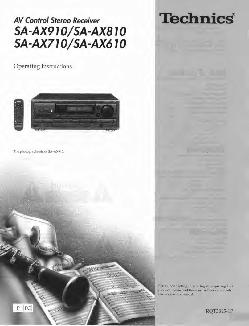
Technics SA-EX300 User manual

Technics

Technics SA-EX300 User manual

Technics SAEX140 - RECEIVER User manual

Technics

Technics SAEX140 - RECEIVER User manual

Technics SA-GX170 User manual

Technics

Technics SA-GX170 User manual

Technics SAEX110 - RECEIVER User manual

Technics

Technics SAEX110 - RECEIVER User manual

Technics SA-AX720 User manual

Technics

Technics SA-AX720 User manual

Technics SA-EX510; SA-EX410; SA-EX310 User manual

Technics

Technics SA-EX510; SA-EX410; SA-EX310 User manual

Technics SA-GX650 User manual

Technics

Technics SA-GX650 User manual

Technics SA-GX350 User manual

Technics

Technics SA-GX350 User manual

Technics SA-5570 User manual

Technics

Technics SA-5570 User manual

Technics SAEX140 - RECEIVER User manual

Technics

Technics SAEX140 - RECEIVER User manual

Technics SA-GX550 User manual

Technics

Technics SA-GX550 User manual

Technics SA-110 User manual

Technics

Technics SA-110 User manual

Technics SA-GX910 User manual

Technics

Technics SA-GX910 User manual

Technics SA-DA10 User manual

Technics

Technics SA-DA10 User manual

Technics SA-GX190 User manual

Technics

Technics SA-GX190 User manual

Technics SA-222 User manual

Technics

Technics SA-222 User manual

Technics SU-CH700 User manual

Technics

Technics SU-CH700 User manual

Technics SA-GX100L User manual

Technics

Technics SA-GX100L User manual

Technics SA-GX670 User manual

Technics

Technics SA-GX670 User manual

Technics SADX930 - RECEIVER User manual

Technics

Technics SADX930 - RECEIVER User manual

Technics SA-DX950 User manual

Technics

Technics SA-DX950 User manual

Technics SA-AX710 User manual

Technics

Technics SA-AX710 User manual

Technics SA-GX505 User manual

Technics

Technics SA-GX505 User manual
Technics SA-5570 User manual

Technics

Technics SA-5570 User manual

Popular Stereo Receiver manuals by other brands

Pioneer SX-434 operating instructions

Pioneer

Pioneer SX-434 operating instructions

Antique Automobile Radio 382201B operating instructions

Antique Automobile Radio

Antique Automobile Radio 382201B operating instructions

Rotel RX-1603 owner's manual

Rotel

Rotel RX-1603 owner's manual

Scott 355R Service manual

Scott

Scott 355R Service manual

Aiwa AV-D58 Service manual

Aiwa

Aiwa AV-D58 Service manual

Pioneer SX-939 Service manual

Pioneer

Pioneer SX-939 Service manual

Denon AVR-887 operating instructions

Denon

Denon AVR-887 operating instructions

Teac AG-H600 Schematic diagrams

Teac

Teac AG-H600 Schematic diagrams

Cambridge Audio AXR85 user manual

Cambridge Audio

Cambridge Audio AXR85 user manual

Teac R-2 Service manual

Teac

Teac R-2 Service manual

The Fisher Gusfom Electro lll operating instructions

The Fisher

The Fisher Gusfom Electro lll operating instructions

Rotel RAP-1580MKII owner's manual

Rotel

Rotel RAP-1580MKII owner's manual

NAD 7220PE 7020e Instructions for installation and operation

NAD

NAD 7220PE 7020e Instructions for installation and operation

Philips DFR150017 Specification sheet

Philips

Philips DFR150017 Specification sheet

Aiwa AV-D78 Service manual

Aiwa

Aiwa AV-D78 Service manual

Rotel RX-802 owner's manual

Rotel

Rotel RX-802 owner's manual

Sony CF-SW07 operating instructions

Sony

Sony CF-SW07 operating instructions

Sony STR-DE197 Easy setup guide

Sony

Sony STR-DE197 Easy setup guide

manuals.online logo
manuals.online logoBrands
  • About & Mission
  • Contact us
  • Privacy Policy
  • Terms and Conditions

Copyright 2025 Manuals.Online. All Rights Reserved.