TESSERA CF-850/F1K-144-S User manual

- 1 -
CF-850/F1K-144-S
Hardware Manual
Date published: Jan 2017 (1st Edition)
Tessera Technology Inc.
TS-TUM05471

- 2 -
CAUTION:
・The information in this document is subject to change without notice.
・No part of this document may be copied or reproduced in any form or by any means without
prior written consent of Tessera Technology Inc.
・Tessera Technology Inc. assumes no responsibility for inaccuracies or misprints of this
document.
・Tessera Technology Inc. does not assume any liability for infringement of patents,
copyrights or other intellectual property rights of third parties by or arising from the use of
Tessera Technology Inc. products listed in this document or any other liability arising from
the use of such products. No license, express, implied or otherwise, is granted under any
patents, copyrights or other intellectual property rights of Tessera Technology Inc. or
others.
・Descriptions of circuits, software and other related information in this document are
provided for illustrative purposes in semiconductor product operation and application
examples. The incorporation of these circuits, software and information in the design of a
customer's equipment shall be done under the full responsibility of the customer. Tessera
Technology Inc. assumes no responsibility for any losses incurred by customers or third
parties arising from the use of these circuits, software and information.

- 3 -
TABLE OF CONTENTS
1INTRODUCTION .................................................................................................................4
2FEATURES...........................................................................................................................5
2.1 CAN ..................................................................................................................................... 6
2.2 SERIAL SELECT ....................................................................................................................... 9
2.2.1
LCD........................................................................................................................... 11
2.2.2
RS-232C.................................................................................................................... 14
2.2.3
USB Serial Conversion ............................................................................................ 15
2.2.4
LIN............................................................................................................................ 16
2.3 PUSH SWITCH ....................................................................................................................... 17
2.4 VOLUME............................................................................................................................... 18
2.5 POWER ................................................................................................................................ 19
2.6 CPU BOARD ........................................................................................................................ 20
2.6.1
Power ........................................................................................................................ 21
2.6.2
CPU........................................................................................................................... 21
2.6.3
Clock ......................................................................................................................... 22
2.6.4
Reset ......................................................................................................................... 22
2.6.5
Switch & LED ......................................................................................................... 23
2.6.6
Debug Connector...................................................................................................... 24
2.6.7
Filter socket.............................................................................................................. 25
2.6.8
Check Pin ................................................................................................................. 25
3CPU TERMINAL CONNECTION LIST.............................................................................26

- 4 -
1Introduction
In this document, features and hardware specifications of CF-850/F1K-144-S, which the 32-bit
single-chip microcomputer RH850/F1K and RH850/F1L from Renesas Electronics Corporation is
mounted, are described.
- 5 -
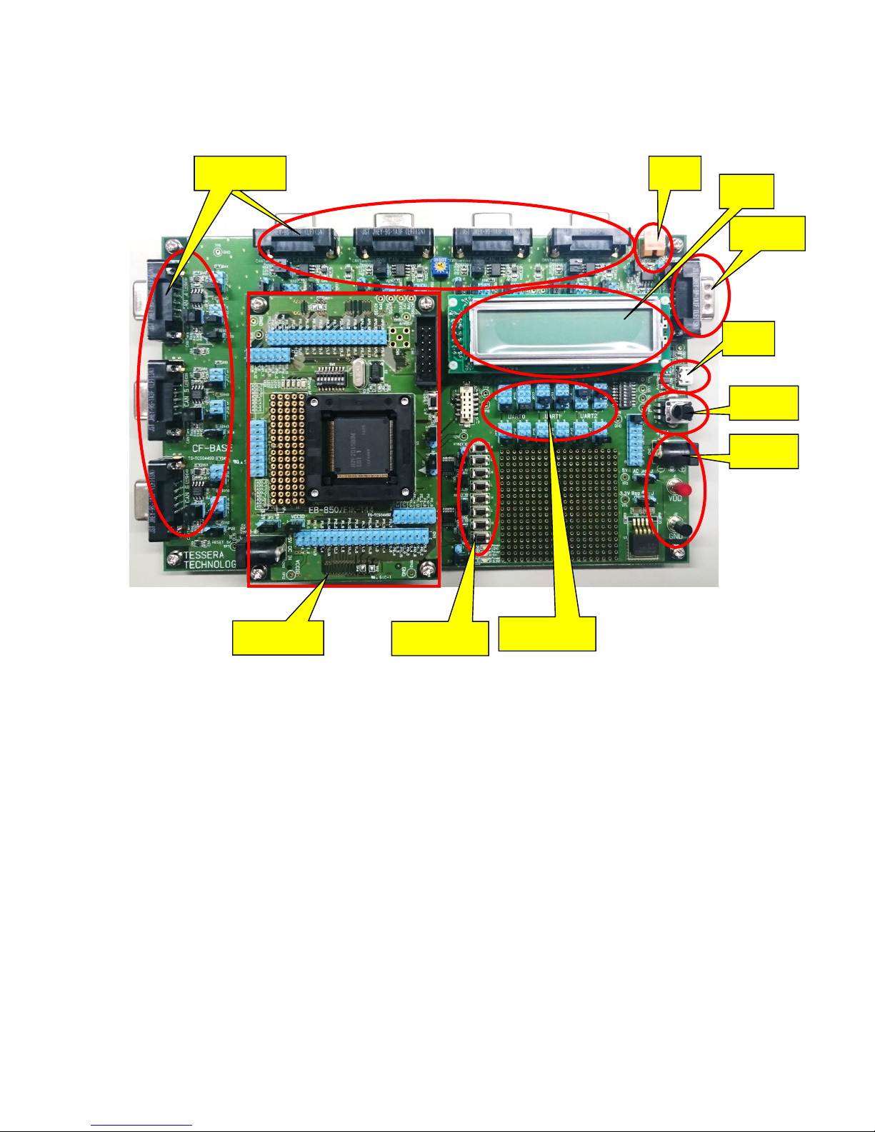
2Features
Volume
Power
RS-232C
USB
CPU Board
Push Switch
Serial select
CAN
LCD
LIN
CAN x 7ch

- 6 -
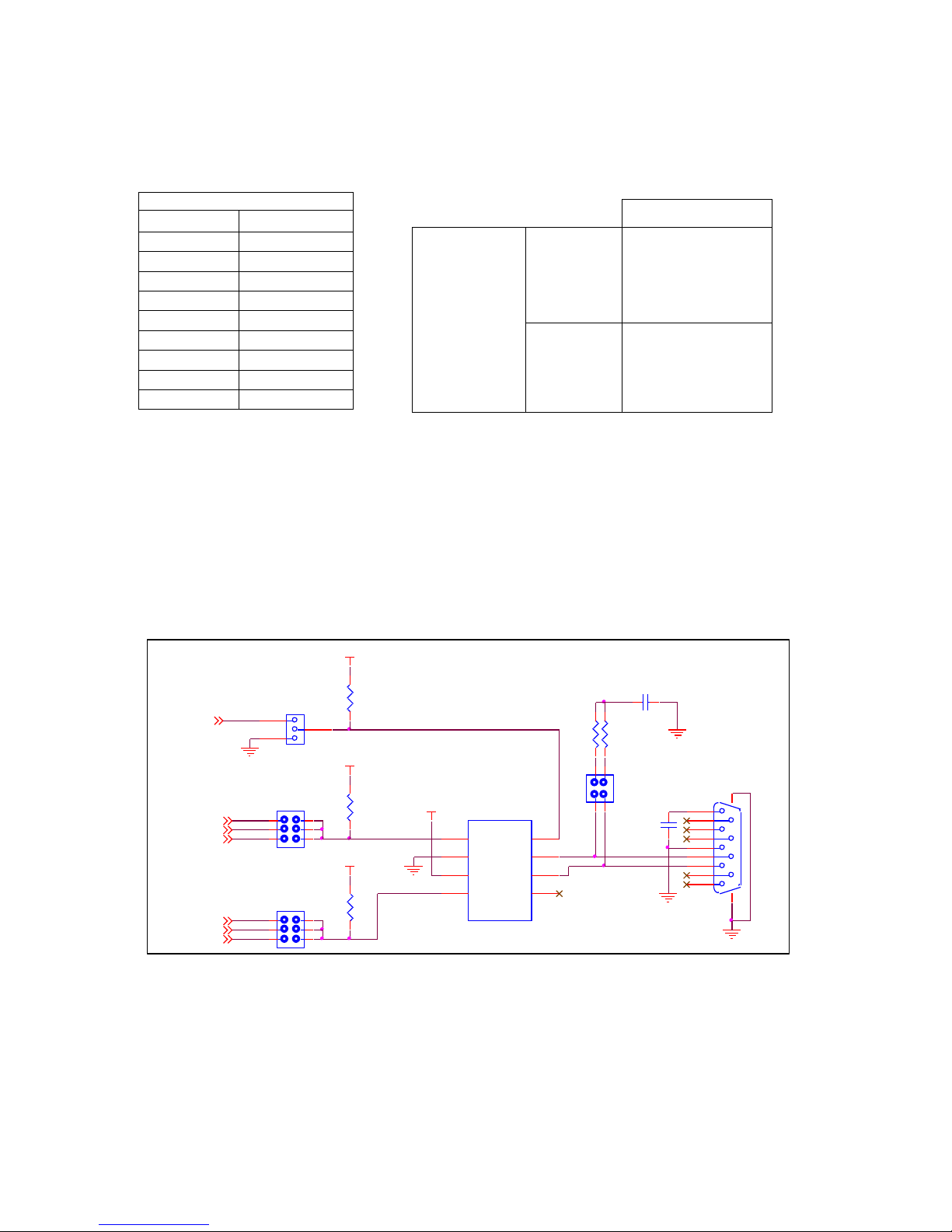
2.1 CAN
The CAN controller of the microcomputer is connected to the CAN FD transceiver
(TJA1044GT). It supports CAN physical layer. Also, CAN bus signal is connected to DSUB 9pin
female connector.
One terminal can be selected by using jumpers from maximum of three multipurpose terminals, and
can be connected to CAN transceiver.
Only one line must be shorted in each jumper.
CAN 0
CAN 1
CAN 2
CAN 3
CAN 4
CAN 5
CAN 6
JP5 (終端抵抗)
JP4 (MODE)
JP6 (TX)
JP7 (RX)

- 7 -
Connecter
P10_1/TAUD0I3/TAUD0O3/CA N0 TX /PWGA1O/TAPA0UN/CSIH1SC/MODE0 1-2
P0_0/TAUD0I2/TAUD0O2/RLIN20RX/CA N0 TX /PWGA10O/CSIH0SSI/DPO 3-4
5-6
P10_0/TAUD0I1/TAUD0O1/CA N0 R X /INTP0/CSCXFOUT/PWGA0O/TAPA0UP/CSIH1SI 1-2
P0_1/TAUD0I4/TAUD0O4/CA N0 R X /INTP0/RLIN20TX/PWGA11O/CSIH0SI/APO 3-4
5-6
P 9 _1 /INTP11/PWGA9O/TAUD0I2/TAUD0O2/KR0I5/CSIH2CSS1/ADCA0I3S MODE0 JP4 1-2
P0_3/TAUD0I8/TAUD0O8/RLIN30RX/INTP10/CA N1 TX /DPIN1/PWGA13O/CSIH0SO 1-2
P10_7/TAUD0I15/TAUD0O15/CSIG0SC/ENCA0TIN1/PWGA4O/ CA N1 TX 3-4
5-6
P0_2/TAUD0I6/TAUD0O6/CA N1 R X /INTP1/RLIN30TX/PWGA12O/CSIH0SC/DPO 1-2
P10_6/TAUD0I13/TAUD0O13/CSIG0SO/ENCA0TIN0/ADCA0SEL2/ CA N1 R X /INTP1/MODE2 3-4
5-6
P 9 _2 /KR0I6/PWGA20O/TAPA0ESO/CSIH2CSS2/ADCA0I9S MODE1 JP8 1-2
P0_4/RLIN31RX/INTP11/CAN 2 TX /PWGA10O/CSIH1SI/SELDP0/DPIN8 1-2
P12_0/CAN2 TX /PWGA56O/TAUB1I10/TAUB1O10 3-4
5-6
P0_5/CAN2 R X /INTP2/RLIN31TX/DPIN9/SELDP1/CSIH1SO 1-2
P11_15/CA N2 R X /INTP2/CSIH2CSS4/PWGA55O/TAUB1I8/TAUB1O8 3-4
5-6
P 9 _3 /KR0I7/PWGA21O/CSIH2CSS3/TAUJ1I1/TAUJ1O1/ADCA0I10S MODE2 JP12 1-2
P0_8/RLIN21TX/DPIN6/CSIH0CSS6/CSIH1SSI/TAUB0I2/TAUB0O2/ CAN3 TX 1-2
P11_4/CSIH2SI/CAN3 TX /PWGA29O/TAUB1I3/TAUB1O3 3-4
P1_3/CAN3 TX /DPIN23 5-6
P0_7/RLIN21RX/DPIN5/CSCXFOUT/CSIH1RYI/CSIH1RYO/TAUB0I0/TAUB0O0/ CA N3 R X /INTP3 1-2
P11_3/CSIH2SC/CAN 3 RX /INTP3/PWGA28O/TAUB1I1/TAUB1O1/RLIN32TX 3-4
P1_2/CAN3 R X /INTP3 5-6
P 9 _4 /CSIH0CSS5/PWGA33O/TAUJ1I0/TAUJ1O0/ADCA0I11S MODE3 JP16 1-2
P0_10/INTP3/CSIH1CSS1/DPIN11/RLIN22TX/TAUB0I6/TAUB0O6/ CAN4 TX 1-2
3-4
5-6
P0_9/INTP12/CSIH1CSS0/DPIN7/RLIN22RX/TAUB0I4/TAUB0O4/ CA N4 R X /INTP4 1-2
3-4
5-6
P 9 _5 /CSIH0CSS6/PWGA34O/TAUJ1I1/TAUJ1O1/ADCA0I12S MODE4 JP20 1-2
P0_14/RLIN32TX/PWGA47O/TAUB0I14/TAUB0O14/CSIG0SC/CAN5 TX 1-2
P11_6/RLIN33RX/INTP13/CAN 5 TX /ADCA1TRG1/PWGA31O/CSIH3SO/TAUB1I7/TAUB1O7 3-4
5-6
P0_13/RLIN32RX/INTP12/PWGA46O/TAUB0I12/TAUB0O12/CSIG0SO/ CA N5 R X /INTP5 1-2
P11_5/CAN5 R X /INTP5/RLIN33TX/PWGA30O/CSIH3SI/TAUB1I5/TAUB1O5 3-4
5-6
P 9 _6 /CSIH0CSS7/PWGA35O/ADCA0I13S MODE5 JP24 1-2
1-2
3-4
5-6
1-2
3-4
5-6
MODE6 JP28 1-2
Default
TxD
JP26
CAN 5
RxD
JP27
TxD
JP30
CAN 6
RxD
JP31
TxD
JP18
CAN 3
RxD
JP19
TxD
JP22
CAN 4
RxD
JP23
TxD
JP10
CAN 1
RxD
JP11
TxD
JP14
CAN 2
RxD
JP15
Jumper
TxD
JP6
CAN 0
RxD
JP7
Following table shows the connection of RH850/F1K.
- 8 -
JP5, JP9, JP13, JP17, JP21, JP25 and JP25 are termination resistor connect. Open or short these
as needed.
About the MODE signal
The MODE signal is connected to the STB terminal of the CAN driver IC (TJA1044GT).
If not controlled by the port, changing the jumper pin to 2-3 short circuit will be fixed to Low, and it
can always be in the normal state.
Connection diagram
From CPU Port
From CPU Port
From CPU Port
From CPU Port
From CPU Port
From CPU Port
From CPU Port
R14
100K
JP4
2
1
3
U5
TJA1044GT
STB 8
Txd
1
Vcc
3GND
2
Rxd
4NC 5
CANL 6
CANH 7
C13
0.1uF
JP7
1 2
3 4
5 6
R16
1.5K
R13
60.4
JP6
1 2
3 4
5 6
R12
60.4
R10
100K
JP5
FFC-4BMEP1
1 2
3 4
C12
4700pF
DSUB1
5
9
4
8
3
7
2
6
1
FG1 FG2
VDD
VDD
VDD
VDD
CAN 0,1,2,3,4,5 DSUB Connector
Pin Number
Signal Name
1
N.C.
2
CANL
3
GND
4
N.C.
5
0.1uFGND
6
N.C.
7
CANH
8
N.C.
9
N.C.
Termination resistor
JP5 : CAN 0
JP9 : CAN 1
JP13:CAN 2
JP17:CAN 3
JP21: CAN 4
JP25: CAN 5
JP29: CAN 6
1-2 Short
3-4 Short
120Ω
1-2 Open
3-4 Open
Non

- 9 -
2.2 Serial select
It can be connected by selecting the microcomputer's UART terminal to "LCD",
"RS-232C", "USB Serial Conversion", and "LIN".
The terminals for using UART can be selected by jumpers.
The connection destination of each UART can be selected with the jumper switch shown
below.
UART0_TXD
JP33
1-2(LCD)
UART0_RXD
JP35
1-2(LCD)
UART1_TXD
JP37
3-4(USB)
UART1_RXD
JP39
3-4(USB)
UART2_TXD
JP41
5-6(RS)
UART2_RXD
JP43
5-6(RS)
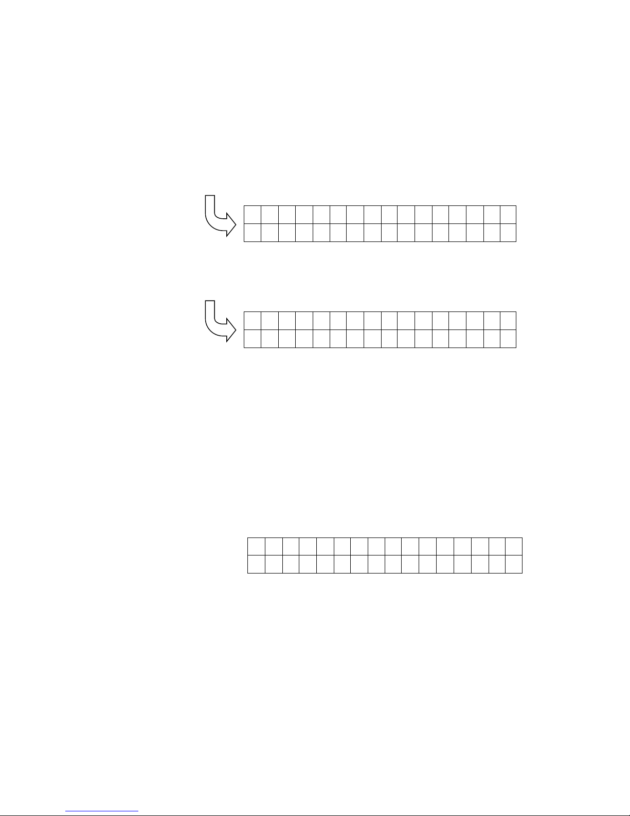
P10_10/TAUD0I14/TAUD0O14/R LI N3 0T X/ENCA0E1/PWGA7O/CSIH0CSS1 1-2
P1_1/R LI N 33 TX 3-4
P11_5/CAN5RX/INTP5/R LI N 33 TX/PWGA30O/CSIH3SI/TAUB1I5/TAUB1O5 5-6
P10_9/TAUD0I12/TAUD0O12/R LI N3 0R X /INTP10/ENCA0E0/PWGA6O/CSIH0RYI/CSIH0RYO 1-2
P1_0/R LI N 33 R X/INTP13 3-4
P11_6/R LI N 33 R X/INTP13/CAN5TX/ADCA1TRG1/PWGA31O/CSIH3SO/TAUB1I7/TAUB1O7 5-6
P10_12/PWGA17O/R LI N 31T X/CSIH1CSS1/TAUB0I3/TAUB0O3 1-2
P1_9/R LI N 34 TX/DPIN20 3-4
P12_2/R LI N 34 TX/PWGA58O/TAUB1I14/TAUB1O14 5-6
P10_11/PWGA16O/R LI N 31R X /INTP11/CSIH1CSS0/TAUB0I1/TAUB0O1 1-2
P1_8/R LI N 34 R X/INTP14 3-4
P12_1/R LI N 34 R X/INTP14/CSIH2CSS5/PWGA57O/TAUB1I12/TAUB1O12 5-6
P10_14/ADCA1TRG0/PWGA19O/R LI N3 2TX /CSIH3SSI/TAUB0I7/TAUB0O7 1-2
P1_5/ADCA1TRG0/R LI N 35 TX/DPIN17 3-4
P11_8/CSIG1SSI/R LIN 3 5TX /PWGA48O/TAUB1I11/TAUB1O11 5-6
P10_13/CSIH0SSI/PWGA18O/R LI N 32 R X/INTP12/TAUB0I5/TAUB0O5 1-2
P1_4/R LI N 35 R X/INTP15 3-4
P11_9/CSIG1SO/R LI N 35R X /INTP15/PWGA49O/TAUB1I13/TAUB1O13 5-6
Default
TxD
UART2
RxD
TxD
UART0
RxD
TxD
UART1
RxD
JP36
JP38
JP40
JP42
JP32
JP34
Short position
Connection destination
1-2
LCD
3-4
USB
5-6
RS-232C
7-8
LIN
JP32, JP34, JP36, JP38, JP40, JP42
JP33, JP35, JP37, JP39, JP41, JP43
- 10 -
Connection diagram
UART0_RXD
JP36
1 2
3 4
5 6
JP32
1 2
3 4
5 6
JP40
1 2
3 4
5 6
JP38
1 2
3 4
5 6
JP42
1 2
3 4
5 6
JP34
1 2
3 4
5 6
From CPU Port UART_USB_TXD
UART_USB_RXD
UART_RS_TXD
UART_RS_RXD
UART_LCD_TXD
UART_LCD_RXD
JP33
1 2
3 4
5 6
7 8
JP35
1 2
3 4
5 6
7 8
JP37
1 2
3 4
5 6
7 8
JP39
1 2
3 4
5 6
7 8
From CPU Port
From CPU Port
JP41
1 2
3 4
5 6
7 8
JP43
1 2
3 4
5 6
7 8
UART0_TXD
UART_LIN_TXD
UART1_TXD
UART1_RXD
UART_LIN_RXD
UART2_TXD
UART2_RXD
From CPU Port
From CPU Port
From CPU Port
From CPU Port
From CPU Port
From CPU Port
From CPU Port
From CPU Port
From CPU Port
From CPU Port
From CPU Port
From CPU Port
From CPU Port
From CPU Port
From CPU Port

- 11 -
2.2.1 LCD
Words can be displayed on LCD panel by sending data to UART that is connected to LCD.
"Binary mode" to display hexadecimal and "ASCII mode" to display ASCII characters can be
selected by the DIP switch (SW1).
Initial screen displays when you press the reset switch on CPU board.
UART Communication Specifications
・Baud Rate 115.2Kbps (Fixed)
・Data Length 8bit (LSB First)
・Parity None
・Stop Bit 1bit
・Flow Control None (continuous transmission enabled)
Binary Mode 1 (SW1_1:ON, SW1_2:ON, SW1_3:Any)
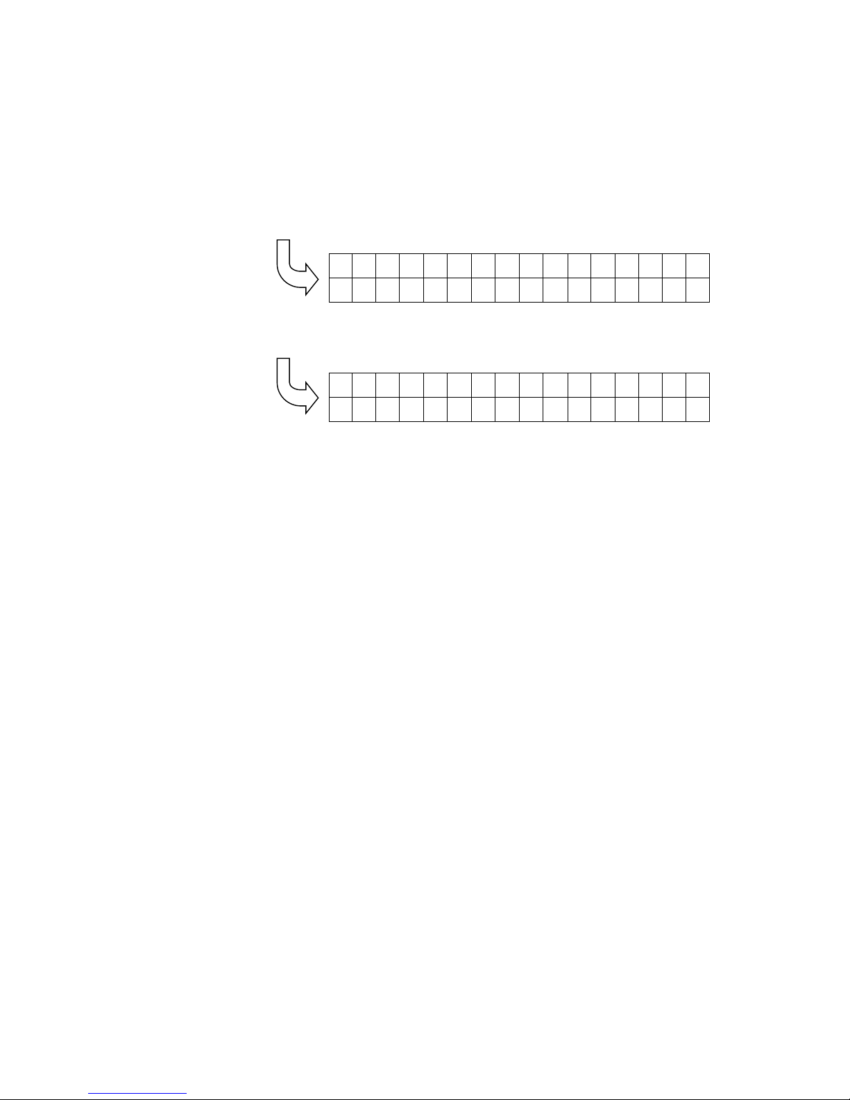
It displays the hexadecimal data as sent with entering space between 1Byte data.
It can display 10Byte in 1 screen. It scrolls 1 line when it received 11Byte of data.
(example)URTH?TX = 0x01; TXWait();
URTH?TX = 0x02; TXWait();
・・・・・・・・・・
URTH?TX = 0x0A; TXWait();
0
1
0
2
0
3
0
4
0
5
0
6
0
7
0
8
0
9
0
A
URTH?TX = 0x10; TXWait();
0
6
0
7
0
8
0
9
0
A
1
0
(use case)By developing a program to send 10Byte once in 1 second, it will display the
first 1Byte at the top-left of the screen.
VR1
Adjust LCD Contrast
SW1
- 12 -
Binary Mode 2 (SW1_1:ON, SW1_2:OFF, SW1_3:ON)
It displays the hexadecimal data as sent without entering space between 1Byte data.
It can display 16Byte in 1 screen. It scrolls 1 line when it received 17Byte of data.
(example)URTH?TX = 0x01; TXWait();
URTH?TX = 0x02; TXWait();
・・・・・・・・・・
URTH?TX = 0x10; TXWait();
0
1
0
2
0
3
0
4
0
5
0
6
0
7
0
8
0
9
0
A
0
B
0
C
0
D
0
E
0
F
1
0
URTH?TX = 0x11; TXWait();
0
9
0
A
0
B
0
C
0
D
0
E
0
F
1
0
1
1
(use case)By developing a program to send 16Byte once in 1 second, it will display the
first 1Byte at the top-left of the screen.
- 13 -
ASCII Mode Ver.2 (SW1_1:OFF, SW1_2:Any, SW1_3:Any)
It displays the characters as sent.
It can display 16 characters in 1 line. It scrolls 1 line when it received 17th character or
linefeed code (0x0D: \r ).
(example)URTH?TX = ‘F’; TXWait();
URTH?TX = ‘l’; TXWait();
・・・・・・・・・・
URTH?TX = ‘T’; TXWait();
F
l
e
x
R
a
y
T
E
S
T
URTH?TX = ‘\r’; TXWait();
URTH?TX = ‘1’; TXWait();
T
E
S
T
1
The position of the cursor can be specified by sending xy-coordinate right after
ESC code (0x1B).
ESC(0x1B) + xy x: 0(0x30)~9(0x39),a(0x61), b, c, d, e, f(0x66)
y: 0(0x30),1(0x31)
(example) printf(buf, “¥x1b00TEST¥x1ba1LCD”);
y
↓
0
T
E
S
T
1
L
C
D
X
→
0
1
2
3
4
5
6
7
8
9
a
b
c
d
e
f
- 14 -
2.2.2 RS-232C
UART that is connected to "RS-232C" can send and receive signals with the RS-232C level of
D-SUB9 pin connector.
Use a cross cable when you connect to PC.
RS-232C D-SUB Connector
Pin Number
Signal
1
N.C.
2
RxD
3
TxD
4
N.C.
5
GND
6
N.C.
7
RTS(N.C.)
8
CTS(N.C.)
9
N.C.
RS-232C

- 15 -
2.2.3 USB Serial Conversion
UART that is connected to "USB serial conversion" can communicate with the COM port of PC
through USB controller (FT230).
If the USB driver is a PC connected to the Internet, the latest driver is automatically installed
by "Windows Update". Please wait until the pop-up "Device is ready to use" appears.
If the driver is not installed, it can be downloaded from the following URL.
http://www.ftdichip.com/Drivers/VCP.htm
Recommended UART communication specification
・Baud rate 115.2Kbps
・Data length 8bit (LSB First)
・Parity None
・Stop Bit 1bit
・Flow Control None
USB1
- 16 -
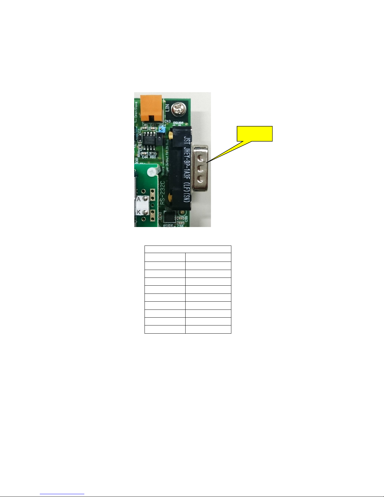
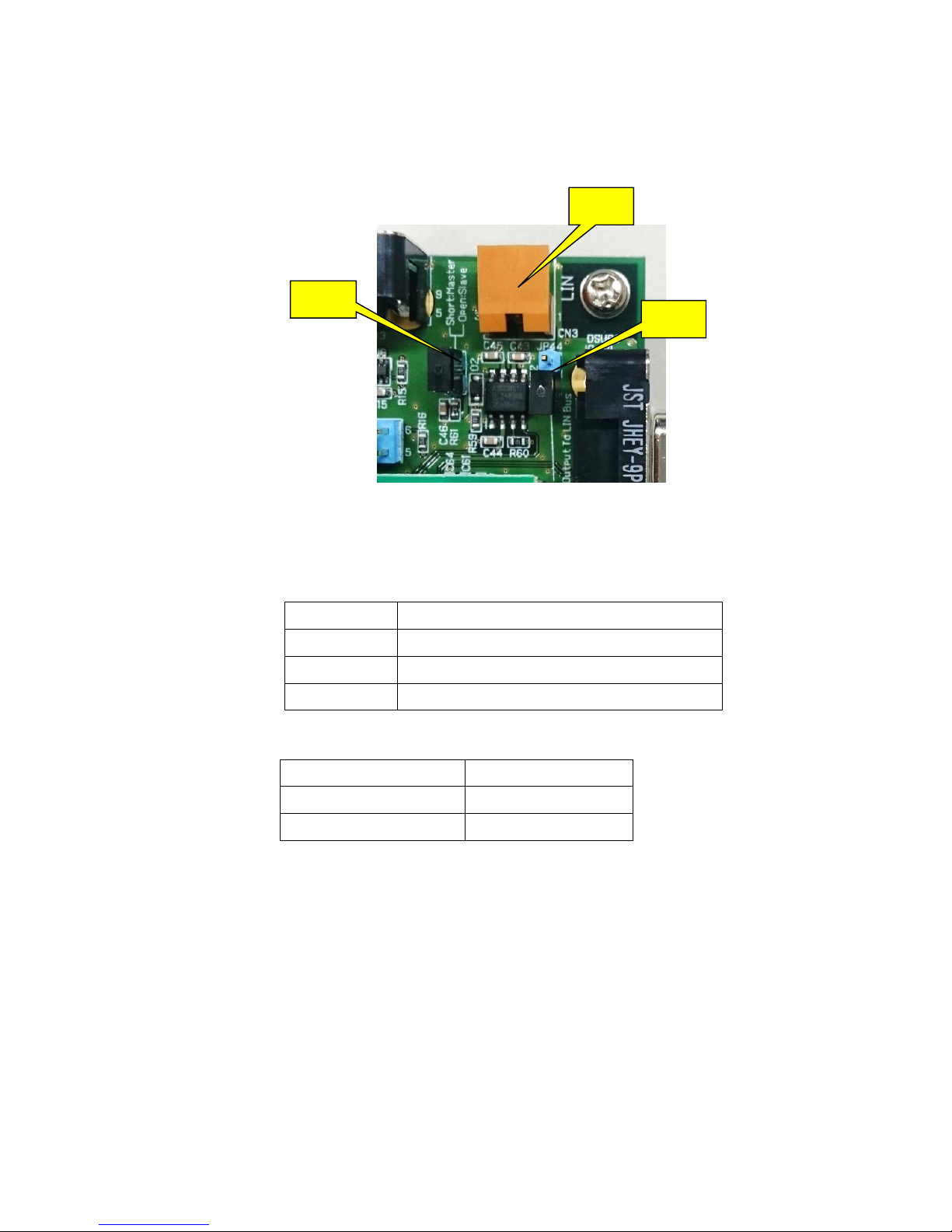
2.2.4 LIN
The UART connected to "LIN" is connected to the LIN compatible transceiver (TJA1020T) and
corresponds to the physical layer of LIN.
Default setting JP44: Open
JP45: Short (LIN Master)
CN3 : IL-G-3P-S3L2-SA (JAE)
JP45
Function
Short
LIN Master
Open
LIN Slave
CN3
Function
1
JP44 short circuit output +12V
2
GND
3
LIN
JP44
CN3
JP45

- 17 -
2.3 Push Switch
4 interrupt signals can be connected to microcomputer's interrupt terminals. The signal can
be set to High by pressing H button, and to Low by pressing L button. It becomes High by reset
signal of the CPU.
Also, it has chattering prevention circuit.
The interrupt signals are disconnected by taking each jumper pin out.
Jumper Switch Signal
P9_0/NMI/PWGA8O/TAUD0I0/TAUD0O0/ADCA0TRG0/CSIH2CSS0/KR0I4/ADCA0I2S NMI JP46:Open SW2/3 SW_NMI
P8_4/TAUJ0I2/TAUJ0O2/DPIN4/CSIH0CSS2/INTP8/PWGA36O/ADCA0I6S INTP8 JP47: Short SW4/5 SW_INTA
P8_3/TAUJ0I1/TAUJ0O1/DPIN3/CSIH0CSS1/INTP7/PWGA23O/ADCA0I5S INTP7 JP49: Short SW6/7 SW_INTB
P8_2/TAUJ0I0/TAUJ0O0/DPIN2/CSIH0CSS0/INTP6/PWGA22O/ADCA0I4S INTP6 JP50: Short SW8/9 SW_INTC
JP46
JP47
JP49
JP50
SW_NMI
SW_INTA
SW_INTB
SW_INTC
- 18 -
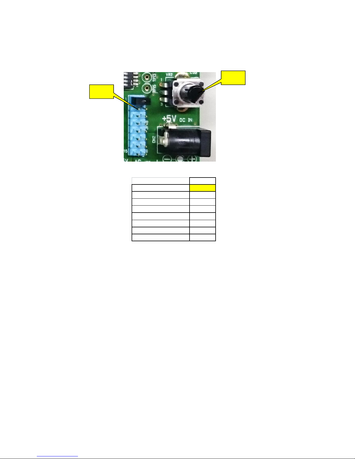
2.4 Volume
It can output variable voltage (0V-IO voltage) to A/D terminal of CPU by variable resistor of 10KΩ.
JP48
AP0_0/ADCA0I0 1-2
AP0_1/ADCA0I1 3-4
AP0_2/ADCA0I2 5-6
AP0_3/ADCA0I3 7-8
AP0_4/ADCA0I4 9-10
AP0_5/ADCA0I5 11-12
AP0_6/ADCA0I6 13-14
AP0_7/ADCA0I7 15-16
VR2
JP48

- 19 -
2.5 Power
Connect bundled AC adapter (+5V) to AC Jack. You do not need to connect to the AC Jack
on the CPU board.
Using the regulator from the power supplied from here, + 12V and + 3.3V are also generated.
Power supply source can be changed by JP2 and JP3.
JP2
5V
1-2
AC adapter
2-3
Terminal
JP3
3.3V
1-2
Regulator
2-3
Terminal
JP1 is the jumper to fix the IO voltage when it does not connect CPU board. Normally, do
not short this.
Terminal: VDD
Terminal: GND
JP3 : 3.3V
AC Jack
JP2 : 5V
Power LED(12V)
Power LED(5V)
Power LED(3.3V)
JP1
- 20 -
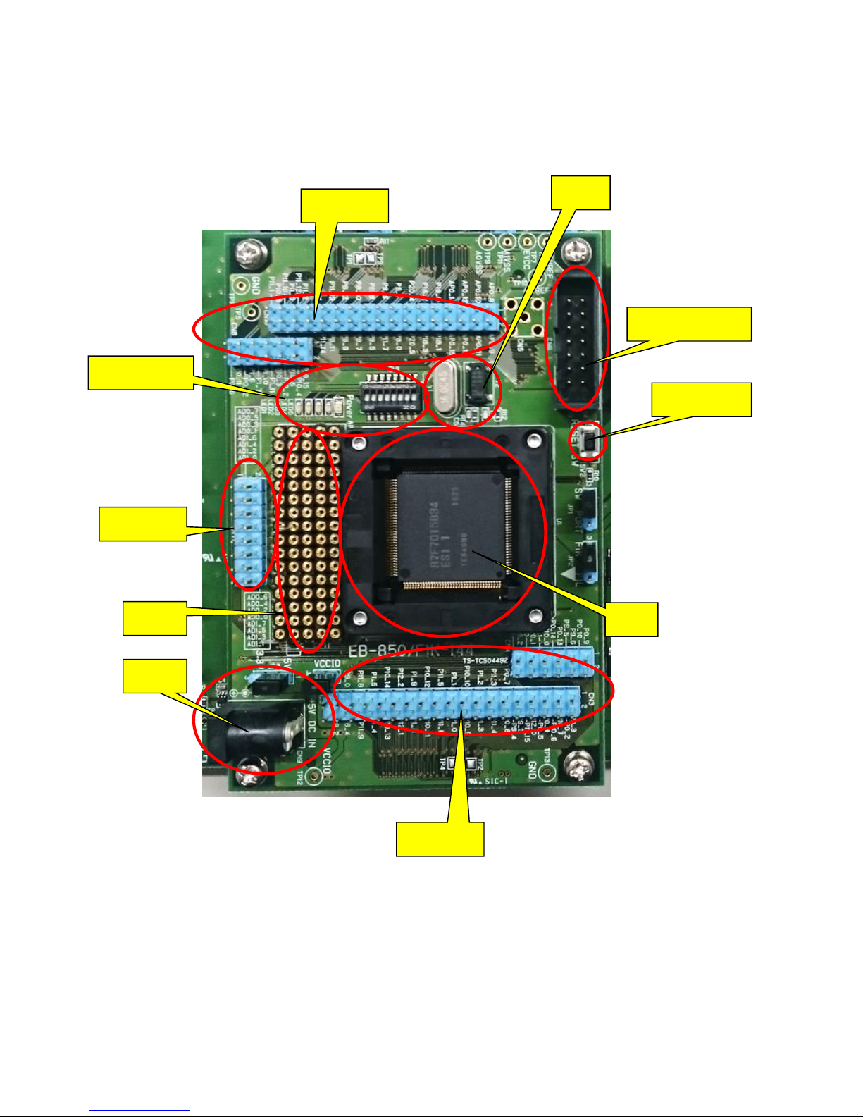
2.6 CPU Board
"EB-850/F1K-144-S" is mounted on the CPU board
Power
Switch & LED
Reset Switch
Debug Connector
Clock
Check pin
Filter
CPU
Check pin
Check pin
Table of contents
Other TESSERA Computer Hardware manuals


Popular Computer Hardware manuals by other brands


Extron electronics
Extron electronics IPL Pro Series user guide

Advantech
Advantech B+B SMARTWORX IE-iMcV-E1-Mux/4 user manual

Belkin
Belkin F5D8071 user manual

Panasonic
Panasonic CF-BAW1024U operating instructions

Nordic Semiconductor
Nordic Semiconductor nRF5340 user guide

Freescale Semiconductor
Freescale Semiconductor TWR-WIFI-G1011MI user manual


