1 Overview
1.1 ADS62PXX EVM Quick-Start Procedure
User's GuideSLAU237A – May 2008 – Revised April 2009
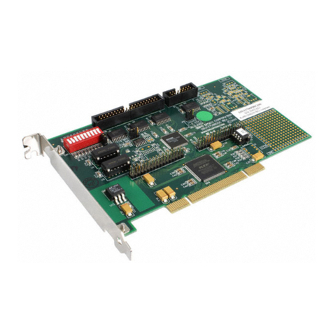
ADS62PXXEVM
This user’s guide gives a general overview of the evaluation module (EVM) and provides a generaldescription of the features and functions to be considered while using this module. This manual isapplicable to the ADS62P42/43/44/45/48/49, ADS62P22/23/24/25/28/29 and ADS62C15/17 analog todigital converters (ADC), which will be collectively referred to as ADS62PXX. This document should beused in combination with respective ADC data sheet. The ADS62PXX EVM provides a platform forevaluating the analog-to-digital converter (ADC) under various signal, clock, reference and power supplyconditions.
The ADS62PXXEVM provides numerous options for providing clock, input frequency and power to theADC under evaluation. The quick start procedure describes how to quickly get initial results using thedefault configuration of the EVM as it was shipped. The EVM can be put back to default configuration bysetting all jumpers to the default positions as described in Table 1 . The default configuration of the EVM isfor the Input Frequency (IF) and the clock input, each to be a single ended input that istransformer-coupled to the ADC. The default configuration for the power supply is to provide a single 5Vsupply to the red banana jack J10, PWR IN. The default configuration for the EVM is to control the modesof operation by jumper settings for parallel input control pins rather than serial SPI control of the registerspace. The other modes of operation of the EVM are described in the latter sections of this document. Ifusers modify the default jumper settings, this procedure does not apply.
A quick-setup procedure for the default configuration of the ADS62PXX follows:
1. Verify all the jumper settings against the schematic jumper list in Table 1 .2. Connect the 5V supply between J10 (PWR IN) and J12(GND). If you are using the TSW1200 forcapture, it also can be used to source 5V for the EVM. To use the 5V output power of the TSW1200,configure JP8 to short 1-2, J22 to short 1-2, and jumper over 5V from the banana jacks on theTSW1200 to J10 on the ADC EVM. Do not connect a voltage source greater than 5.5V.3. Switch on power supplies.4. Using a function generator with 50 Ωoutput impedance, generate a 0V offset, 1.5V
PP
sine-wave clockinto J19. The frequency of the clock must be within the specification for the device speed grade.5. Use a frequency generator with a 50 Ωoutput impedance, generate a 0V offset, –1 dBFS-amplitudesine-wave signal into J6 (Channel A) or J3 (Channel B).This provides a transformer-coupled differentialinput signal to the ADC.6. Connect the TSW1200 or suitable logic analyzer to J8 to capture the resulting digital data. If aTSW1200 is being used to capture data, follow the additional alphabetically labeled steps. For moredetails, see Connecting to FPGA Platforms , located in this document.a. After installing the TSW1200 software and connecting the TSW1200 to the USB port, open theTSW1200 software.b. Depending on the ADC under evaluation, select from the TI ADC Selection pull-down menu.c. Change the ADC Sample rate and ADC Input frequency to match those of the signal generator.d. After selecting a Single Tone FFT test, press the Capture Data button.
Windows is a registered trademark of Microsoft Corporation.
6ADS62PXXEVM SLAU237A – May 2008 – Revised April 2009Submit Documentation Feedback
