1.3 EVM Basic Functions
EVM Overview
1.2.2 Reference Voltage
The 4.096-V precision voltage reference is provided to supply the external voltage reference and sets thevoltage output range of the DAC under test through REF3140, U3, via jumper W4 by shorting pins 1 and2. The test point TP4 as well as J4-20 are also provided to allow the user to connect to other externalreference source if the onboard reference circuit is not desired. The external voltage reference should notexceed the applied power supply, V
DD
, of the DAC under test.
The REF3140 precision reference is powered by +5VA through J6-4 or J5-3 (if installed) terminal.
CAUTIONWhen applying an external voltage reference through TP4 or J4-20, makesure that it does not exceed the DAC7554 power supply (V
DD
) maximum.Otherwise, this can permanently damage the DAC7574, U1, device undertest.
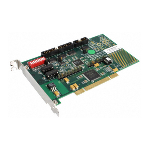
The DAC7554 EVM is designed primarily as a functional evaluation platform to test certain functionalcharacteristics of the DAC7554 DAC. Functional evaluation of the DAC device can be accomplished withthe use of any microprocessor, TI DSP or some sort of a waveform generator.
The headers J2 and P2 are the connectors provided to allow the control signals and data required tointerface a host processor or waveform generator to the DAC7554 EVM using a custom built cable.
An
adapter
interface
card
(5-6k
adapter
interface)
is
also
available
to
fit
and
mate
with
TI’s
TMS320C5000™ and TMS320C6000™ DSP Starter Kit (DSK). This alleviates the hassle involved inbuilding a custom cable. In addition, there is also an MSP430 based platform (HPA449) that uses theMSP430F449 microprocessor, with which this EVM can connect and interface. For more details orinformation regarding the 5-6k adapter interface card or the HPA449 platform, call Texas Instruments orsend email to [email protected].The DAC outputs can be monitored through the selected pins of J4 header connector. All the outputs canbe switched through their respective jumpers W2, W11, W12 and W13, for the reason of stacking.Stacking allows a total of eight DAC channels to be used provided that the SYNC signal is unique for eachEVM board stacked. The SYNC signal must be decoded for the specific EVM, therefore, the decodershould be implemented but can only be done externally from the EVM board.
In addition, the option of selecting one DAC output that can be fed to the noninverting side of the outputoperational-amplifier, U2, is also possible by using a jumper across the selected pins of J4. If two EVMsare stacked together, the output operational-amplifier's noninverting input, are shorted together at the J4header. Alterations to the traces are necessary to use the U2 features. The traces for J4-1, J4-3, J4-5,and J4-7 are visible from the topside of the EVM. However, one issue still remains, the trace to thenoninverting pin of U2 cannot be seperated from J4-1. Therefore, only one of the stacked EVMs can beused with the U2 feature. Finally, the output operational-amplifier, U2, must first be configured correctly forthe desired waveform characteristic to be seen. See section 4 of this user’s guide.
A block diagram of the EVM is shown below in the Figure 1 .
DAC7554EVM 6 SLAU154 – March 2005
