2 3. Features of This EVM
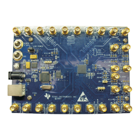
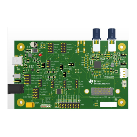
The EVM has the following features:
• Four power supply decoupling capacitors from VDD to Ground (2 × 3.3 µF, 1 µF, 0.1 µF)
• One additional power supply decoupling capacitor pad from VDD to Ground (0.1 µF)
• One power supply decoupling capacitors from VSS to Ground (2 × 3.3 µF, 1 µF, 0.1 µF)
• One additional power supply decoupling capacitor pad from VDD to Ground (0.1 µF)
• Protection diode pads available near VDD and VSS input.
• 10 µF supply decoupling capacitor to Ground on both VFP and VFN supplies
• Protection diode pads available near VFP and VFN inputs
• Up to four auxiliary pathways available with jumpers
• Up to eight analog I/O pathways available
• All analog I/O pathways have pads available to load device
• All analog I/O pathways have pads available to support SMA connections to device.
• Fault indicator flag LED circuit included on EVM
3 4. TMUX741-746EVM Setup
1. If the default conditions on the board isn’t what you desired please refer to the following table to set up the
Auxiliary pathways which can be either VFP,VFN,SEL,DR, or NC depending on device installed.
Jumper on Pathway Possible Signal Pull Up Resistor
Pad ID
Load Resistor Pad
ID
Load Capacitor Pad
ID
Additional
Capacitor Pad ID
J7 VFN / SEL R4 R17 C17 C10
J5 VFN / SEL N/A N/A N/A N/A
J8 VFP / SEL R6 R18 C18 C9
J6 VFP / SEL N/A N/A N/A N/A
J9 DR / SEL R7 R19 C19 N/A
J10 NC / SEL R8 R20 C20 N/A
2. If VFP and VFN are used in the application, attach a shunt on J5 and J6 to the appropriate VFP/VFN source.
3. Next, use the following table to set up the desired configuration of the analog channels:
Jumper on Pathway Pull Down Resistor
Pad ID
Pull Up Resistor
Pad ID
Load Resistor Pad
ID
Load Capacitor Pad
ID
TVS Diode Pad ID
J11 R33 R21 R34 C21 D6
J12 R35 R22 R36 C22 D7
J13 R37 R23 R38 C23 D8
J14 R39 R24 R40 C24 D9
J15 R53 R41 R54 C25 D10
J16 R55 R42 R56 C26 D11
J17 R57 R43 R58 C27 D12
J18 R59 R44 R60 C28 D13
4. Next, solder down the chosen TMUX74xx in either a PW or QFN package that is to be tested.
5. If using dual supplies, connect shunt from VSS to PAD on J19.
6. If using single supplies, connect shunt from VSS to GND on J4.
7. Next, power the board through J2. Follow the specific device data sheet as to what range the voltage should
be set to.
8. If VFP/VFN pins are used in the application and are using an external source power this through J3.
9. If the fault flag voltage (VFF) is used in the application, connect and power up this source through J1.
3. Features of This EVM www.ti.com
4TMUX741xEVM and TMUX746EVM User's Guide SCDU019 – JUNE 2021
Submit Document Feedback
Copyright © 2021 Texas Instruments Incorporated
