Total Phase Level Shifter User manual

Level Shifter Board
Features
• Level shifting of I C, SPI, and MDIO signals from 1.2 V to 3.3 V
• I C speeds of up to 800 kHz
• SPI and MDIO speeds of up to 20 MHz
• Powering downstream devices
• Multiple voltage options
Summary
The Level Shifter Board expands the utility of all of Total Phases I C,
SPI, and MDIO products by allowing developers to communicate,
analyze, and power downstream devices of lower logic levels.
Supported products:
Level Shifter Board
User Manual v1.01
March 13, 2017
2
2
2
(注1)
(注意)
AardvarkをLevelShifterBoardのAdapter/Analyzerコネクタに接続して使用する場合、
Aardvarkがハングアップしてソフトの再起動やUSBの着脱が頻繁に必要になることがあります。
これは、Aarvarkの改造で発生しないようにすることができます。弊社にご相談ください。
LevelShifterBoardのTARGETLEDは、単にTarget側(Level変換後)の回路へ電源が来ているか
どうかだけを示しています。ロットにも依存しますが点灯時の明るさの違いは無視してください。
(注1)LevelShifterBoardのTARGET電源出力を外部で利用する場合の注意点。
1.2Vか1.5Vの設定では、電源ON(5V入力)の瞬間、出力電圧が1.8V程度になることが
あります。それが問題になる場合は、弊社に改造等をご相談ください。
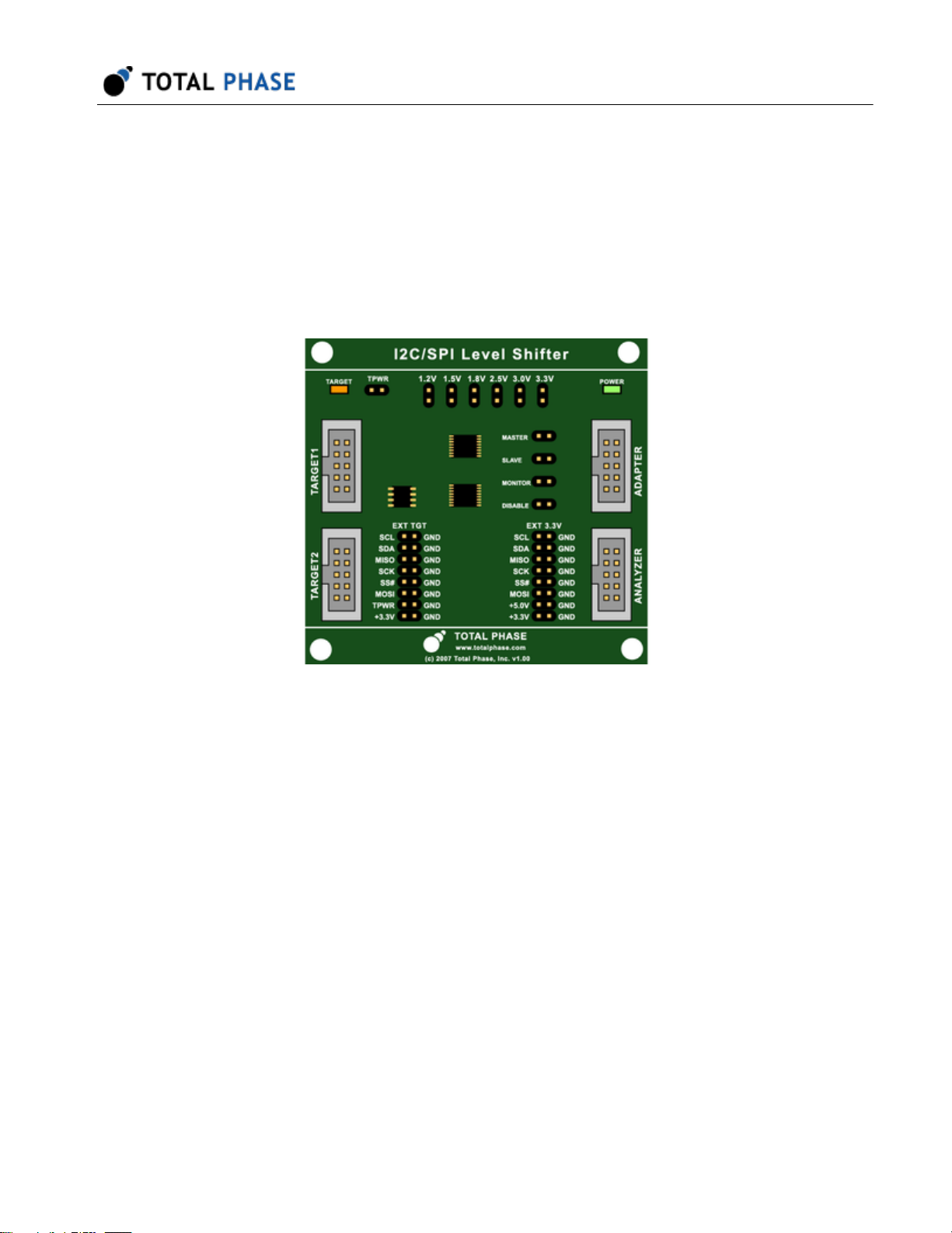
1 Overview
The Level Shifter Board provides embedded systems engineers with an easy and cost-
effective method for interfacing Total Phase's products with lower logic level devices. The
Level Shifter Board is capable of down-shifting to all standard logic levels from 1.2 V to
3.3 V. Engineers can also choose to power downstream devices.
Figure 1 : Schematic of the Flash Socket Board
1.1 Features
• Level shifting for I C, SPI, MDIO, and GPIO signals.
• On-board regulator to specify and power downstream devices to 1.2 V, 1.5 V,
1.8 V, 2.5 V, 3.0 V, and 3.3 V.
1.2 What's Included
The Level Shifter Board comes complete with:
• (1) Level Shifter Board
• (1) 6.0-inch 10-pin ribbon cable
Level Shifter Board User Manual v1.01
2
2

• (1) 1.5-inch 10-pin ribbon cable
• (3) jumpers for configuration
Level Shifter Board User Manual v1.01
3

2 Hardware Specification
2.1 Power Consumption
The power consumption of the Level Shifter Board depends on its configuration. The
board will draw approximately 6 mA from the Adapter/Analyzer side when configured to
power the target device, and approximately 4 mA when the target is supplying its own
power.
The current draw of the Level Shifter Board on the Target side is only applicable when
the target device is supplying power to the board. This current draw will be approximately
1 mA.
2.2 Speed
The Level Shifter Board is rated for I C communication at up to 800 kHz.
Maximum SPI and MDIO signaling rates are highly dependent on the specific
configuration of the level shifting board and the timing specification of the target device.
The Level Shifter Board has been tested to operate at up to 18 MHz when shifting to
1.2 V, and up to 20 MHz when shifting to 3.3 V. When operating at higher speeds,
shorter cables are recommended to help maintain signal integrity.
Please note that individual results will vary.
2.3 I C Pull-up Resistors
The Adapter/Analyzer side will always require pull-up resistors for I C communication.
This is easily accomplished by using the built-in pull-up resistors of either an Aardvark I
C/SPI Host Adapter or Beagle I C/SPI/MDIO Protocol Analyzer. Additionally, any I C line
that is being used as a digital input line (GPIO) to the Adapter/Analyzer side, must also
include a pull-up on the adapter side.
It is recommended that pull-up resistors are always used on the Target side I C lines.
Users may find that they can still communicate properly without these pull-ups; however,
Level Shifter Board User Manual v1.01
2
2
2
2
2 2
2
4

it is recommended that pull-ups to the target's logic high still be used to ensure that the
signal reaches its correct level.
2.4 Leakage Voltage
The Level Shifter Board is known to leak approximately 0.2 V to the Target side, even
when configured to not supply power to the target. This is a very weak leakage which is
only capable of sourcing approximately 20 µA of current.
2.5 Board Dimensions
The dimensions of Level Shifter Board are in inches. The mounting holes are 0.187
inches diameter. The figure (Figure 2 ) shows the relevant measurements.
Figure 2 : Dimensioned Level Shifter Drawing
Level Shifter Board User Manual v1.01
5
注2製造ロットによっては、Figure2の横方向サイズが1.27mm長くなっています。
これは穴中心から側面への長さが0.15インチ(3.81mm)ではなく、0.2インチ(5.08㎜)
に左右のどちらかが長くなっていることによります。この場合横方向の全体長さが
3インチ(76.2mm)ではなく3.05インチ(77.47mm)になります。ご了承ください。
この伸びた部分は電気回路には影響しません。
注2
注2

3 Connectors
3.1 ADAPTER and ANALYZER
There are two boxed connectors on the right side (Adapter/Analyzer side) of the Level
Shifter Board (Figure 3 ) which are used to connect the board to an Aardvark I C/SPI
Host Adapter, Cheetah SPI Host Adapter, and/or Beagle I C/SPI/MDIO Protocol
Analyzer. These two connectors are cross-connected, so it does not matter which one is
used. In most cases, you will only want to connect a single adapter at a time to the Level
Shifter Board.
Figure 3 : Two boxed connectors for connecting an adapter
and/or analyzer to the Level Shifter Board.
The second connector may be used to connect a second host adapter. Examples of
these situations are: in order to have more slaves, or to create a multi-master situation.
Alternatively, the second connector can be used to connect a protocol analyzer. For
example, an Aardvark adapter or a Cheetah adapter can be connected to the board
through the ADAPTER connector to program a low-voltage memory chip. At the same
time, a Beagle I C/SPI/MDIO Protocol Analyzer can be attached to the ANALYZER
connector to monitor the bus while the chip is being programmed to ensure that the data
on the bus is correct.
The pinout of the two connectors is described in Figure 4.
Level Shifter Board User Manual v1.01
2
2
2
6

Figure 4 : The pinout for the two boxed connectors on the
Adapter/Analyzer side of the Level Shifter Board.
3.2 TARGET1 and TARGET2
There are two boxed connectors on the left side (Target side) of the Level Shifter Board
(Figure 5 ) which are used to connect the target bus to the level shifter. The signal lines
on these connectors are operating at the voltage levels specified by the user. This level
can either be specified on the board through the use of the jumper connectors, or can be
determined by the downstream system. These two connectors are cross-connected, so it
does not matter which one is used.
Level Shifter Board User Manual v1.01
7
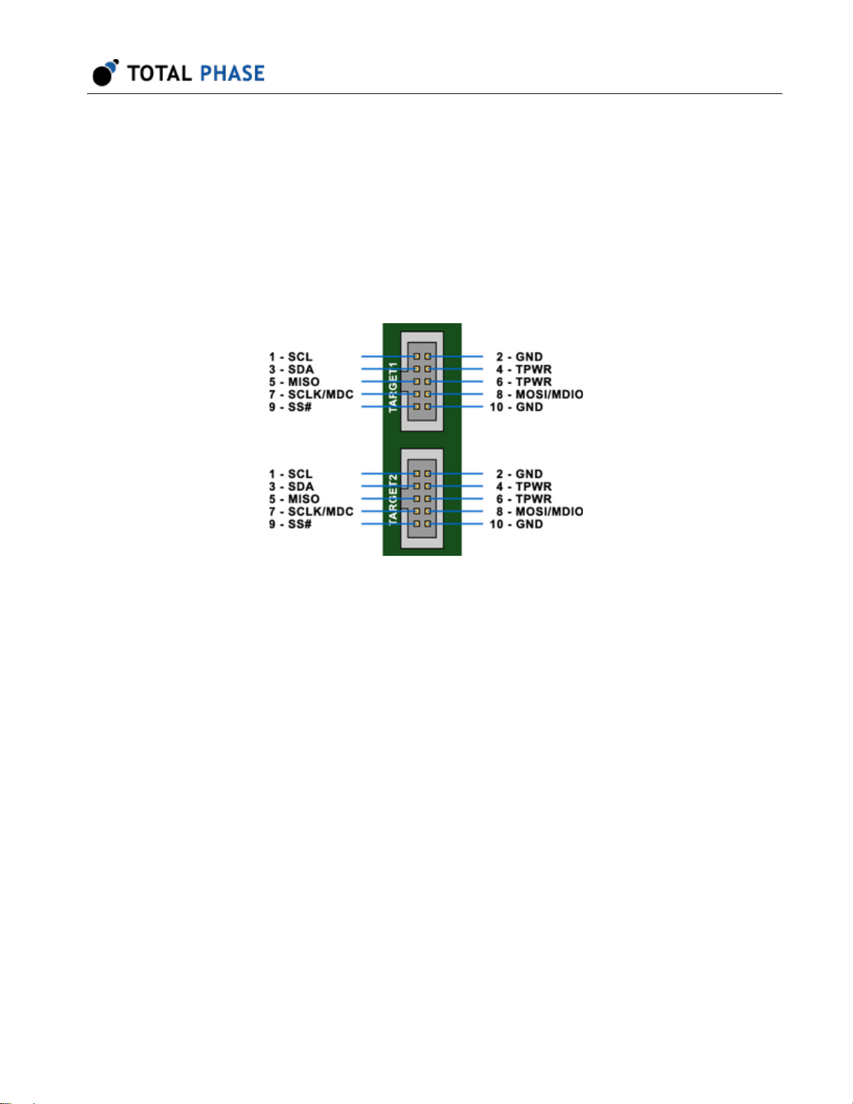
Figure 5 : Two boxed connectors for connecting the Level
Shifter Board to one or more target buses.
These two boxed connectors have an almost identical pinout to the ADAPTER and
ANALYZER connector. The only difference is that the 5.0 V pins will have the target's
voltage level instead.
The pinout of the two connectors is described in Figure 6.
Figure 6 : The pinout for the two boxed connectors on the
Target side of the Level Shifter Board.
3.3 EXT 3.3V and EXT TGT
All the bus and power signals on the board are also available through two 16-pin
headers on the board (Figure 7}. The EXT 3.3 V connector provides the bus signals at
the standard signaling levels employed by Total Phases I C, SPI, and MDIO products.
The EXT TGT connector provides the bus and power signals of the downstream device
and will be at the voltage level defined by the user. All connections are labeled for the
user's convenience.
Level Shifter Board User Manual v1.01
2
8

Figure 7 : The External Connectors provide the developer
with a quick and easy way to interface or monitor any or all
of the Level Shifter Board signals on either the Adapter/
Analyzer side or the target side.
3.4 Powering the Level Shifter Board
In order to function properly, both sides of the board must be powered. The Adapter/
Analyzer side (the high voltage side) must be powered with 5 V. This can easily be
accomplished by using the target power feature of Total Phases I C, SPI, or MDIO
products when it is connected to the Adapter/Analyzer side of the board. Target power
can be enabled via the Rosetta Language Bindings, the Flash Center software, the
Aardvark Control Center Software, the Beagle Data Center software, or the Cheetah GUI
Software.
When powered-on, the board's green POWER LED will be lit.
The Target side (the low voltage side) can optionally be powered by the power already
supplied to the Level Shifter Boardor by the target device. If powering the Target side by
the target device, simply connect the device's power to the TPWR pin on the EXT TGT or
either one of the TARGET boxed connectors (Figure 8 ).
Level Shifter Board User Manual v1.01
2
9
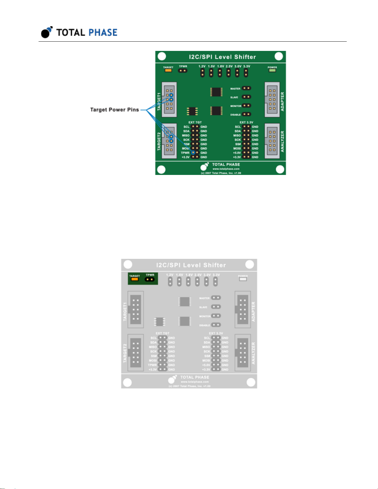
Figure 8 : When powering the Target side of the Level
Shifter Board, power needs to be supplied to one of these
Target power pins.
If powering the Target side by the power already supplied on the board, then a jumper
must be placed to enable this feature (Figure 9 ). Refer to Section 4 for more details.
Figure 9 : When supplying power from the Level Shifter
Board to the target, a jumper needs to be place on TPWR.
When the Target side is properly powered, the board's amber TARGET LED will be lit.
Level Shifter Board User Manual v1.01
10

3.5 Cross Connecting Aardvark Adapters and/or Cheetah
Adapters
When cross connecting two adapters, the board must be powered on. Otherwise, results
may be unpredictable. If you experience problems, please make sure that the POWER
LED on the board is lit.
Level Shifter Board User Manual v1.01
11
4 Configuring the Level Shifter
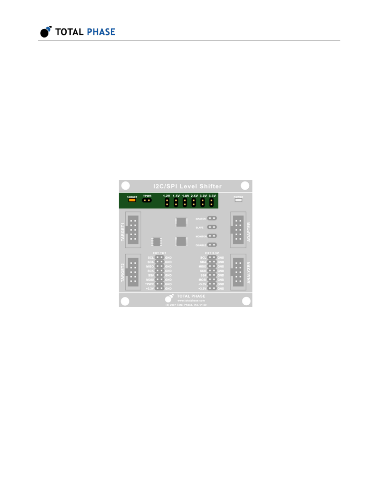
4.1 Selecting Shifting Level
There are two options for selecting the Target side logic level.
The first method is to use the power supplied to the Level Shifter Board to power the
target device. In this method, the output voltage must be enabled by placing a jumper on
the TPWR pins. Then a second jumper is used on one of the voltage selection pins
illustrated in Figure 10. The pins are clearly labeled with the output voltage that they will
set. If no jumper is set on these pins, then it will default to 1.2 V.
Figure 10 : A jumper must be placed on the appropriately
labeled header for the desired voltage level. If supplying
power from the Level Shifter Board to the target, a jumper
needs to be place on TPWR as well.
The second method is to match the power supplied to the Target side when using a self-
powered device/board. When using this option, the logic levels will be set to match the
voltage levels applied to TPWR as shown in Figure 8.
In this configuration, the TPWR jumper must be removed. Simply connect the power and
ground of the target device to the power and ground of the Level Shifter Board Target
side. In order to function properly, the target's voltage level should not exceed 3.3 V.
Level Shifter Board User Manual v1.01
12

4.2 I C Level Shifting
The I C level shifting circuit automatically handles the bi-directionality of I C
communication. Simply select the correct logic level (as described previously) and
correctly connect the SCL and SDA lines of the master and slave.
4.3 SPI Level Shifting
Unlike I C, the SPI level shifting logic must be explicitly controlled for direction. The four
headers on the right side of the board determine the direction of traffic. Selections are
made by placing a jumper on one of the headers. Their uses are described below:
Figure 11 : The Level Shifter Board must be configured
from the correct mode of operation when using this board to
interface with an SPI or an MDIO bus.
•MASTER: When selected, will configure the Adapter/Analyzer side of the board to
behave as the SPI master. Thus, the SS#, SCK, and MOSI lines will be shifted
down to the Target side logic level. The MISO line will be left in its default enabled
state, and will be shifted up to the Adapter/Analyzer's logic level.
•SLAVE: When selected, will configure the Adapter/Analyzer side of the board to
behave as the SPI slave. Thus, the MISO line will be shifted down to the Target
Level Shifter Board User Manual v1.01
2
2 2
2
13

side logic level. The SS#, SCK, and MOSI line will be left in their default enabled
state, and will be shifted up to the Adapter/Analyzer's logic level.
•MONITOR: When selected, will leave all SPI lines in their default enabled state,
and will therefore be shifted up to the Adapter/Analyzer side logic level. This
option is used in situations where only a Beagle I C/SPI/MDIO analyzer is
plugged into the board, and no SPI adapter is being used.
•DISABLE: When selected, will disable all Target side SPI outputs, and set them to
a high-impedance state. If no connection is set, the board will default to this state.
However, if any of the previous configuration is set, it will take precedence on this
one.
It is important to note that for most all cases only one of these connections should be set
at a time. Using more than one may cause incorrect SPI operation. The only situation in
which more than one jumper may be used is if the SPI lines are being used for GPIO.
4.4 MDIO Level Shifting
The MDIO signal lines are shared with SPI. It is therefore not possible to bidirectionally
shift MDIO signals, as the SPI level shifting does not have the infrastructure for this.
However, MDIO monitoring of lower logic levels is still possible. Simply place the SPI
control jumper on MONITOR, and set the Beagle I C/SPI/MDIO analyzer to monitor
MDIO.
4.5 GPIO Level Shifting
GPIO signals may fall on either I C lines or SPI lines, and each of these situations must
be handled separately. When the GPIO lines coincide with the SPI lines, special care
must be taken to ensure that the SPI level shifting circuit is configured to the correct
direction. The SPI lines are logically broken up into two separate groups: the master-
driven lines (SS#, SCK, MOSI) and the slave-driven line (MISO). The direction of each of
these groups can be controlled independently, but all signals within a group will be in the
same direction.
Placing a jumper on the MASTER header will enable the master-driven lines to down-
shift, and the slave-driven line to up-shift. Placing a jumper on the SLAVE header will
enable the slave-driven line to down-shift, and the master-driven lines to up-shift. Placing
a jumper on the MONITOR header will enable all lines to up-shift. If there is ever a time
when a line is configured to be both up-shifting and down-shifting, the down-shift will
take precedence. Thus, if you want to use all the SPI lines as digital outputs from the
host adapter, simply place jumpers on both the MASTER and SLAVE headers.
Level Shifter Board User Manual v1.01
2
2
2
14
注3つまりMDIO用としては、低電圧のMDIOバスを3,3Vレベルに一方向だけレベルシフトするmonitor用途
しか想定していません。MDIOマスタデバイスまたはスレーブデバイスのレベルシフトを行いたい場合、
立野電脳(株)へご相談ください。

The I Clines do not require any directional configuration as it is a bi-directional bus. Each
I C line may go in a different direction, and can also be swapped on the fly.
Level Shifter Board User Manual v1.01
2
2
15

5 Legal / Contact
5.1 Disclaimer
All of the software and documentation provided in this datasheet, is copyright Total
Phase, Inc. ("Total Phase"). License is granted to the user to freely use and distribute the
software and documentation in complete and unaltered form, provided that the purpose
is to use or evaluate Total Phase products. Distribution rights do not include public
posting or mirroring on Internet websites. Only a link to the Total Phase download area
can be provided on such public websites.
Total Phase shall in no event be liable to any party for direct, indirect, special, general,
incidental, or consequential damages arising from the use of its site, the software or
documentation downloaded from its site, or any derivative works thereof, even if Total
Phase or distributors have been advised of the possibility of such damage. The software,
its documentation, and any derivative works are provided on an "as-is" basis, and thus
come with absolutely no warranty, either express or implied. This disclaimer includes, but
is not limited to, implied warranties of merchantability, fitness for any particular purpose,
and non-infringement. Total Phase and distributors have no obligation to provide
maintenance, support, or updates.
Information in this document is subject to change without notice and should not be
construed as a commitment by Total Phase. While the information contained herein is
believed to be accurate, Total Phase assumes no responsibility for any errors and/or
omissions that may appear in this document.
5.2 Life Support Equipment Policy
Total Phase products are not authorized for use in life support devices or systems. Life
support devices or systems include, but are not limited to, surgical implants, medical
systems, and other safety-critical systems in which failure of a Total Phase product could
cause personal injury or loss of life. Should a Total Phase product be used in such an
unauthorized manner, Buyer agrees to indemnify and hold harmless Total Phase, its
officers, employees, affiliates, and distributors from any and all claims arising from such
Level Shifter Board User Manual v1.01
16

use, even if such claim alleges that Total Phase was negligent in the design or
manufacture of its product.
5.3 Contact Information
Total Phase can be found on the Internet at http://www.totalphase.com/. If you have
support-related questions, please go to the Total Phase website. For sales inquiries,
©2008-2017 Total Phase, Inc.
All rights reserved.
Level Shifter Board User Manual v1.01
17
Table of contents
Other Total Phase Test Equipment manuals


