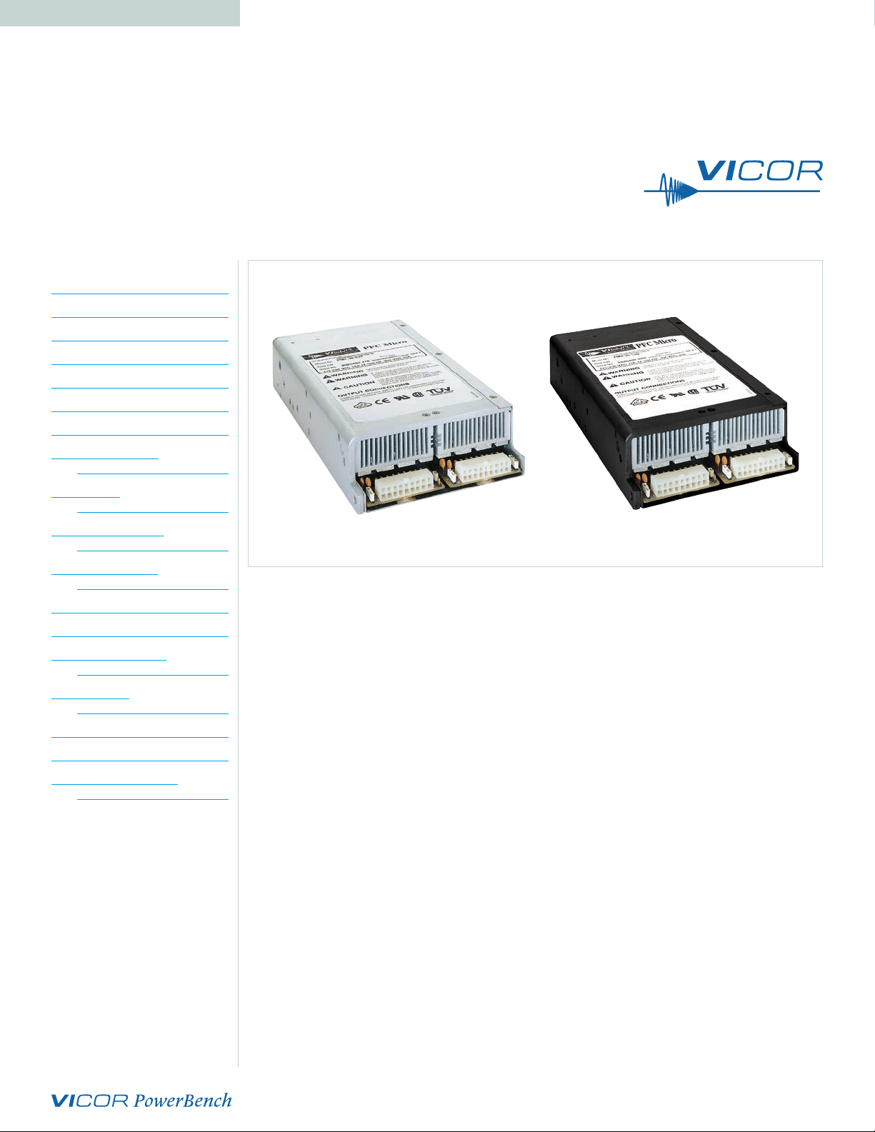
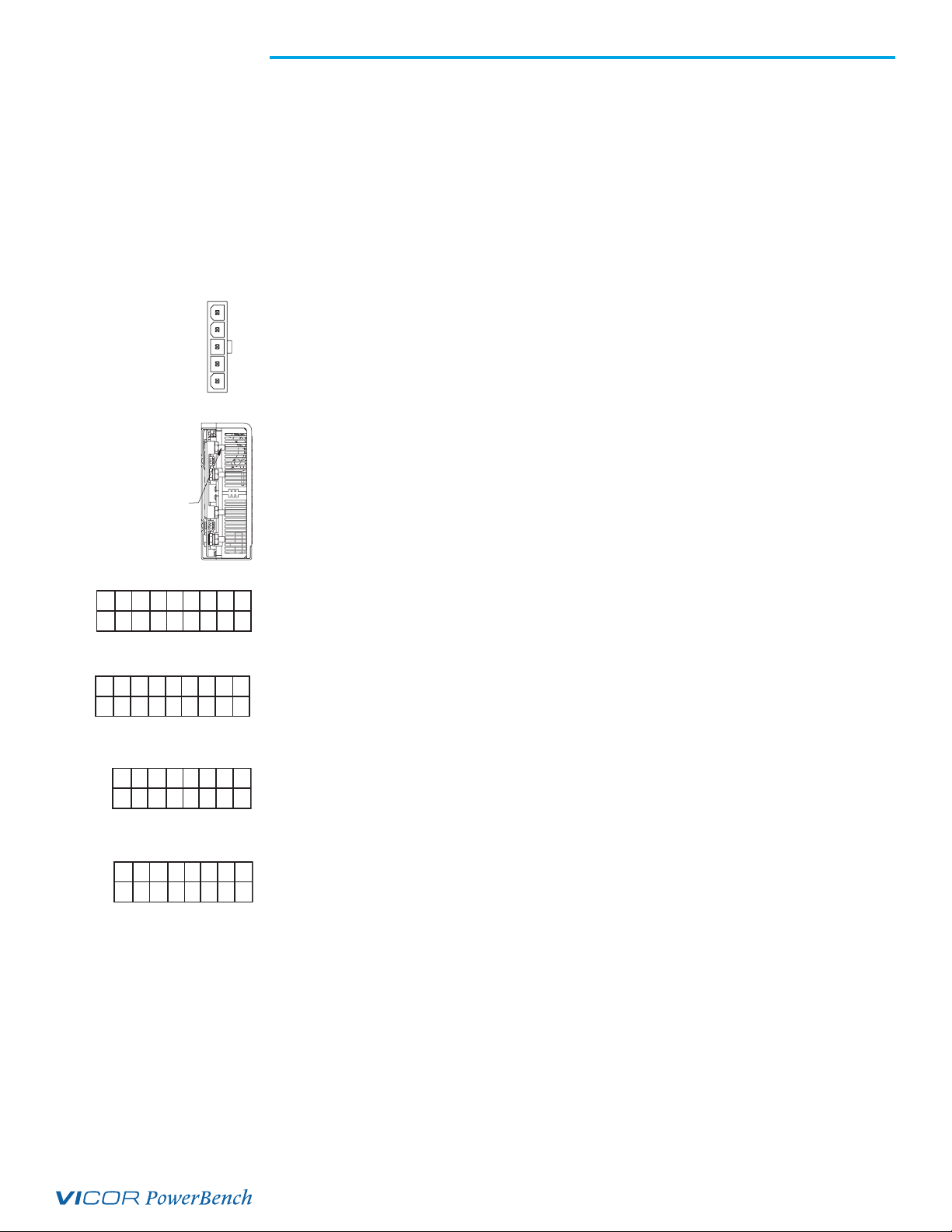
VICOR PFC Micro User manual

UG:121 Page 1
Overview
The PFC Micro is a low-profile switching power supply that combines the advantages of power factor
correction (PFC) and high power density. This guide covers both standard and rugged COTS (MI)
versions of the supply. A PFC Micro provides up to six isolated outputs (from two slots) and each slot
may accommodate the following Vicor DC-DC Converters:
VE-200™/VE-J00™ Series: 1 VE-200 or 2 VE-J00
Maxi/Mini/ Micro Series: 1 Maxi, 2 Minis, or 3 Micros
The use of these converters gives the PFC Micro the inherent power flexibility typical of all Vicor
products. Accepting input voltages of 85 – 264VAC, and 100 – 300VDC, the PFC Micro can provide
up to 800W in a package size of 1.86 x 5.06 x 10.40in [47,3 x 128,5 x 264,1mm]. The PFC Micro is
factory-configured to meet user output requirements.
Contents Page
Overview 1
Standard Features 2
Optional Features 2
Part Numbering 3
Mechanical Considerations 3
PFC Micro Dos and Don’ts 3
Technical Description 4
PFC Micro™ Quick
Install Instructions 5
PFC Micro™
Mechanical Drawings 7
Output Connections
for the PFC Micro™ 8
Output Connectors
for PFC Micro™ 9
Power Connections 9
User Interface Connections 11
Module Power Good
Status Mode 11
Single-Output
Power Supplies (Arrays) 15
Specifications 16
Output Power De-Rating 19
Current Share Boards –
Optional Feature 21
PFC Micro™
Power Factor Corrected AC-DC Switcher
USER GUIDE | UG:121

UG:121 Page 2
Standard Features
Power Factor Correction: Typically 0.98 (>75% Load)
Universal Input: 85 – 264VAC, 47 – 500Hz, or 120 – 300VDC
Power Output: 800W at 230VAC (200VAC minimum input); 500W at 115VAC (100VAC minimum input)
Up to six isolated outputs (two slots)
Fan cooled
Full power to 45°C; half power at 65°C
Soft start for limiting inrush current
Conducted EMI: FCC Class A; EN55022 Class A (consult factory)
Harmonic Distortion to EN61000-3-2
AC Power OK status signal
RoHS compliant available
Output Sequencing and General Shut Down
Autosense (Refer to pages 6 and 14 for more information on Autosense)
Output overcurrent protection on all outputs
Output overvoltage protection and output overtemperature limiting
(not applicable when using VI-J00)
Ride-through (hold-up) time: >20ms at 500W load
Size: 1.86 x 5.06 x 10.4in [47,3 x 128,5 x 264,1mm]
Safety Agency Approvals: CE Marking, TÜV CUE (certain models may not have all listed approvals)
Uses 300VDC input VI-200™/VI-J00™ modules and/or 375VDC input Maxi/Mini/Micro modules
Power good status signal when Maxi, Mini, or Micro modules used
Optional Features
I/T/H-Grade output converters
Current Share Board for unit to unit power sharing - see pages 22 – 23
Connector kits (# 19-130044)
MI Chassis Specific
Mil-STD 810 for Shock and Vibration
Mil-STD 704 and 1399 for overvoltage and transients
–40°C operation
Conformal coating - contact factory

UG:121 Page 3
Part Numbering
PFC Micro PCx1-x2x3(-x4)-xxxx-x5
ex: PC6-06-5012-G
x1= number of outputs
x2= number of VI-200™/VI-J00™ modules
x3= number of Maxi/Mini/Micro modules
(-x4) = optional Factory assigned
xxxx = sequential number assigned by Vicor
x5= optional versions
Note: x5= MI for rugged chassis, = MC for rugged chassis with conformal coating
Mechanical Considerations
The PFC Micro™ can be mounted on one of three surfaces using standard 8-32 or 4mm screws.
Maximum allowable torque is 5in.lbs and the maximum penetration of 0.25in [6mm] on the sides and
0.125in [3mm] on the bottom.
When selecting a mounting location and orientation, the unit should be positioned so air flow is not
restricted. Maintain a 2in [5,1cm] minimum clearance at both ends of the PFC Micro and route all cables
so air flow is not obstructed. The power supply draws air in at the fan side/AC input side and exhausts
air out the load side. If air-flow ducting is used, avoid sharp turns that could create back pressure. The
fan moves approximately 10CFM of air.
Avoid excessive bending of output power cables after they are connected to the output terminals.
For high-current outputs, use cable ties to support heavy cables and minimize mechanical stress on
connectors. Be careful not to short-out to neighboring outputs. The maximum torque recommended on
output nuts is 10in.lbs.
Avoid applications in which the unit is exposed to excessive shock or vibration levels as the unit
is designed primarily for office type equipment. In such applications, a shock-absorbing mount
design is required.
PFC Micro Dos and Don’ts
Do not restrict airflow to the unit. The cooling fan draws air into the unit and forces it out at
the output power terminals. A minimum of two inches in front and behind the supply should be
maintained in order to prevent air obstructions.
Run the output (+/–) power cables next to each other to minimize inductance.
Do not attempt to repair or modify the power supply in any manner. In the event of problems,
contact Customer Service at 1-800-735-6200.
Insert proper fault protection at power supply input terminals (i.e., a fuse).
Use proper size wires to avoid overheating and excessive voltage drop.
Output voltages over 60VDC, whether from individual modules or series arrays, are considered
as hazardous secondary outputs under UL 60950. Appropriate care must be taken in design
implementation of the supply.

UG:121 Page 4
Technical Description
The PFC Micro™ consists of an off-line single-phase, power-factor-corrected front end, EMI filter,
cooling fan, customer interface, power supply control circuit, associated housekeeping circuits and a
selection of Vicor VI-200™/VI-J00™ and/or Maxi DC-DC converters.
Input AC mains voltage is applied to input connector MB1J1. The input current is passed through an
EMI filter designed to meet conducted noise limit "A" specifications of FCC Part 15.
At start up, inrush current is limited by a PTC thermistor. The PTC is shunted out shortly after initial
power up by a DC bus voltage sense circuit driving a relay. After rectification, the input voltage is put
through a boost converter that keeps the AC input current sinusoidal and synchronized with the input
AC voltage (in compliance with EN61000). The boost converter delivers a regulated input to the hold-up
capacitors and a high-voltage backplane. The backplane supplies power to the DC-DC converters that
provide the desired low voltage regulated outputs.
Output voltage conversion is achieved by the Vicor family of Zero-Current Switching (ZCS) DC-DC
converters. These are forward converters in which the main switching element switches at zero current.
This patented topology has a number of unique attributes: low switching losses; high-frequency
operation, resulting in reduced size for magnetics and capacitors; excellent line and load regulation;
wide adjustment range for output; low EMI/RFI emission and high efficiencies.
At initial power up, the PFC Micro outputs are disabled to limit the inrush current and to allow the
DC bus potential to settle out to the correct operating level. A low-power flyback converter converts
the high-voltage DC bus into regulated low voltage to power the internal housekeeping circuits and
DC cooling fan.
The internal housekeeping VCC comes up within 1s after the application of input power. Once the
high-voltage bus is within operating limits, the AC Power OK signal asserts to a TTL "1," indicating the
input power is OK, and the power outputs will come up 250ms later.
An output enable / disable function is provided to control Vicor DC-DC converters. If the Enable/Disable
control pin is pulled low, the modules output is disabled. The nominal delay associated for an output to
come up when measured from release of the Enable/Disable pin is 9 – 12ms. The General Shut Down
function controls all outputs simultaneously and works in a similar manner.
Line Filter Bridge
Rectifier Soft Start
Circuit Boost Converter
PFC Control
Power Supply
Control
Output Card #1
Output Card #2
Fan
Isolated
Housekeeping
Power Supply
Customer
Interface
Power
Output
Power
Output
Input
Enable/Disable -Power Good Read
Figure 1
PFC Micro architecture

UG:121 Page 5
PFC Micro™ Quick Install Instructions
(For Mechanical Drawing, see page 7)
Mounting the PFC Micro
The PFC Micro can be mounted on either of three sides.
Use #8-32 or 4mm mounting screws. Maximum penetration should not exceed 0.25in [6 mm]
on the side and 0.125in [3mm] on the bottom.
Maintain 2in [5,1cm] clearance at both ends of power supply for air flow.
Input Connections
Input Power MBJ1
Apply input AC power connector MBJ1.
Maximum torque is 5in.lbs.
A fuse or circuit breaker in the input line is necessary for safety requirements (10A).
Molex mating receptacle 39-01-4051, terminals 39-00-0090, crimp tool Molex # 11-01-0199.
Output Connections
Note: Outputs with current molex connectors are limited to 9A/pin (27A per output).
A PFC Micro with DIFFERENT Molex connectors capable of 40A is available. Contact factory.
Power Connections
Installing bus bars on output studs (when full-size module is used):
The right stud is Positive and the left stud is the Return on single output cards.
Remove the nut and place ring lug over output stud.
Replace and tighten the nut to a torque of 10 inch pounds.
Do Not over-tighten nuts.
Installing power connectors with 18-pin Molex connectors (when half-size module used):
S1/S2 J1-7, S1/S2 J1-8 and S1/S2 J1-16 are Positive for output #1, while pins
S1/S2 J1-9, S1/S2 J1-17 and S1/S2 J1-18 are the Returns.
S1/S2 J1-1, S1/S2 J1-10 and S1/S2 J1-11 are Positive for output #2, while pins
S1/S2 J1-2, S1/S2 J1-3 and S1/S2 J1-12 are the Returns.
For this 18-pin housing, use Molex mating receptacle #39-01-2180 with #39-00-0039 terminals.
Attach 18 – 24AWG stranded wire using Molex tool #11-01-0197.
Installing power connectors with 16-pin Molex connectors (when quarter-size modules used):
S1/S2 J1-7 and S1/S2 J1- 15 are Positive for output #1, while pins
S1/S2 J1-8 and S1/S2 J1- 16 are the Return.
S1/S2 J1-4 and S1/S2 J1-12 are Positive for output #2, while pins
S1/S2 J1-5 and S1/S2 J1- 13 are the Return.
S1/S2 J1-1 and S1/S2 J1-9 are Positive for output # 3, while pins
S1/S2 J1-2, and S1/S2 J1-10 are the Returns.
For this 16-pin housing, use Molex mating receptacle #39-01-2160 with #39-00-0039 terminals.
Attach 18 – 24AWG stranded wire using Molex tool #11-01-0197.
MBJ1-5 PIN
Not Connected
GND
L2/N
L1
Not Connected
MAXI MODULE
(2 ISOLATED OUTPUTS)
-
+
-
+
S1
S2
10-32 STUDS
9 8 7 6 5 4 3 2 1
18 17 16 15 14 13 12 11 10
S1/S2 J1
- + + T - + - - +
- - + - T + - + +
S1/S2 J1 (18 Pin)
8 7 6 5 4 3 2 1
16 15 14 13 12 11 10 9
S1/S2J1
- + T - + T - +
- + T - + N/C- +
S1/S2J1 (16 Pin)

UG:121 Page 6
Sense Connections
Sense connections on output connections with studs:
The PFC Micro™ is shipped with Autosense installed
(For more information on Autosense, refer to page 14)
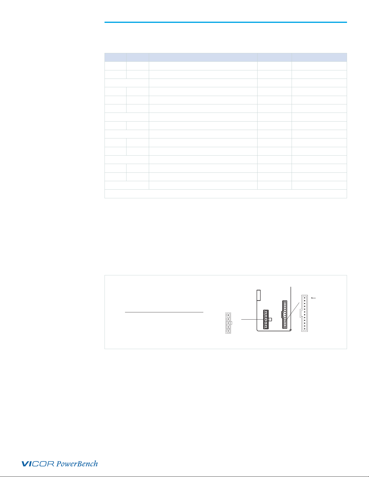
For remote sense, connect remote-sense wires to remote-sense/trim-pin access connector S1/S2 J2.
Connector pin S1/S2 J2-2 is the +SENSE and
S1/S2 J2-3 is the –SENSE.
Use Molex mating receptacle #50-57-9403 with #16-02-0103 terminals.
Attach terminals to 24 – 30AWG stranded twisted pair wire using Molex tool #11-01-0208.
Attach opposite end of sense lines to their respective outputs to point where regulation is desired.
Verify that sense lines are not cross-connected.
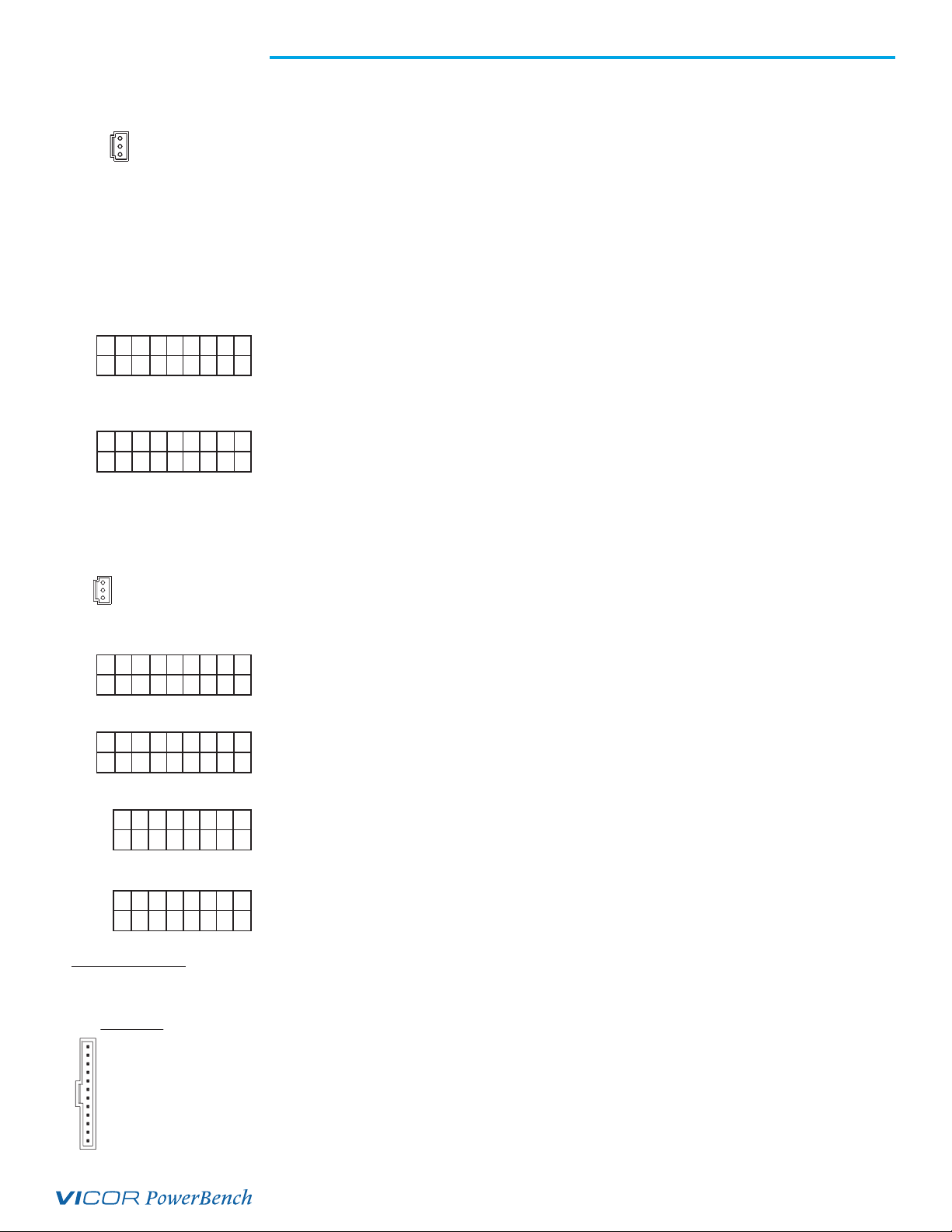
Sense connections on output connections with 18-pin Molex connectors:
The PFC Micro is shipped with Autosense installed
(For more information on Autosense, refer to page 14)
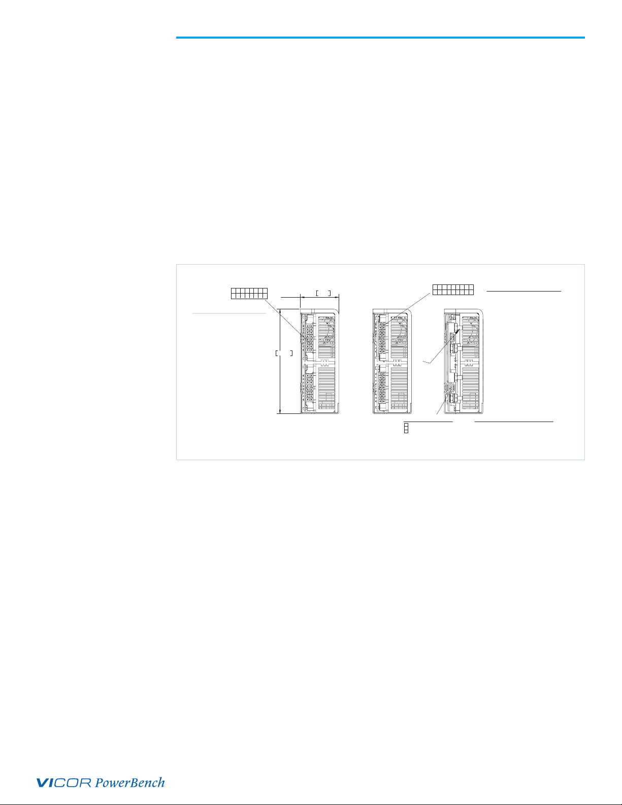
If remote sense is desired, connect remote sense wires to sense lines of Connector S1/S2 J1.
Connector pin S1/S2 J1-13 is the +SENSE and
S1/S2 J1-15 is the –SENSE for output #1.
S1/S2 J1-4 is the +SENSE and
S1/S2 J1-5 is the –SENSE for output #2.
Use Molex mating receptacle #39-01-2180 with #39-00-0039 terminals.
Attach 18 – 24AWG stranded twisted pair wire using Molex tool #11-01-0197.
Note: Remote sense is NOT available for triple-output slots.
Trim Connections
Trim connections on output with studs:
S1/S2 J2-1 provides trim access.
Use Molex mating receptacle #50-57-9403 with #16-02-0103 terminals.
Attach 18 – 24AWG stranded wire using Molex tool #11-01-0208.
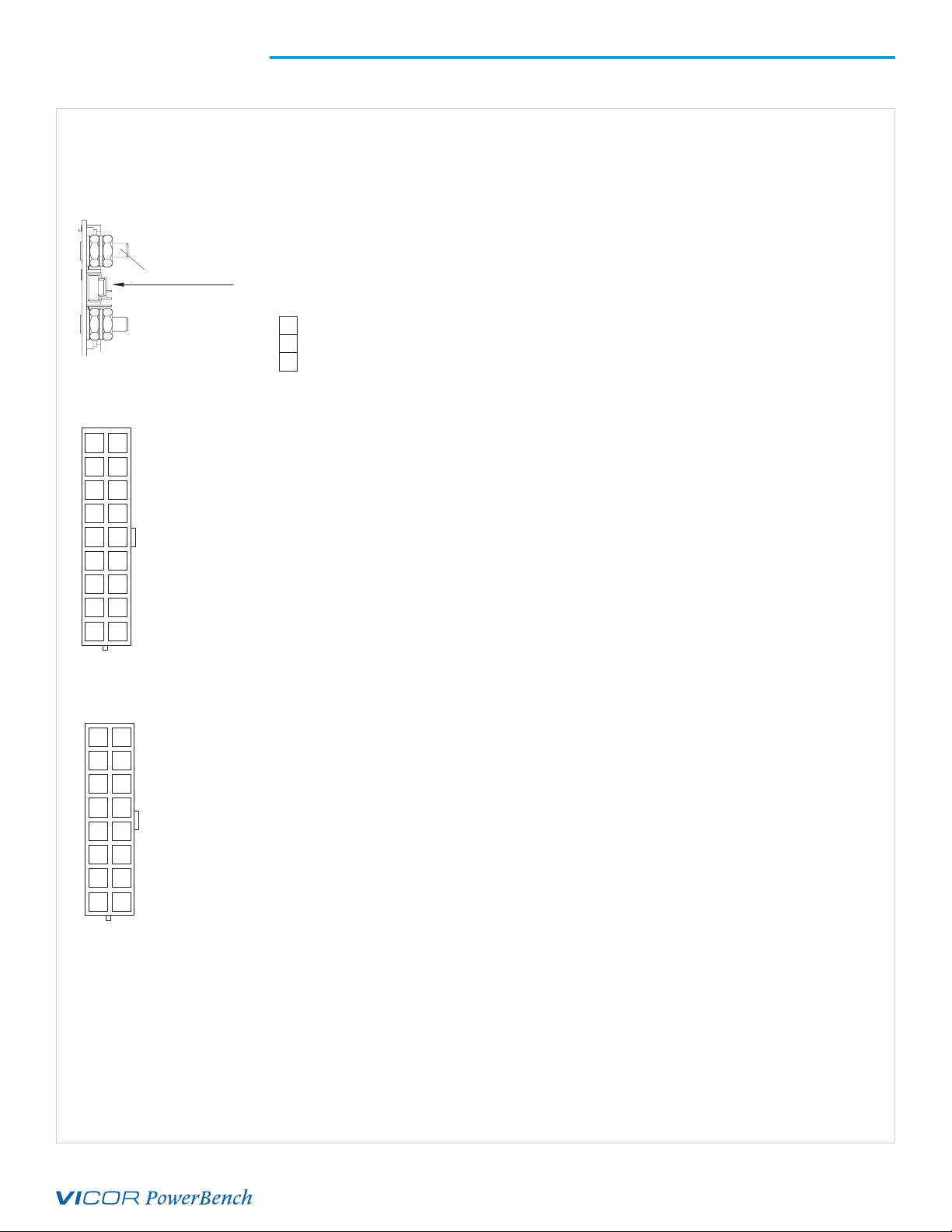
Trim connections on connector with 18-pin molex connectors:
S1/S2 J1-6 provides trim access for output #1, and
S1/S2 J1-14 provides trim access for output #2.
Use Molex mating receptacle #39-01-2180 with #39-00-0039 terminals.
Attach 18 – 24AWG stranded wire using Molex tool #11-01-0197.
Trim connections on connectors with 16-pin Molex connectors:
S1/S2 J1-14 provides trim access for output #1, and
S1/S2 J1-6 provides trim access for output #2, and
S1/S2 J1-3 provides trim access for output #3.
Use Molex mating receptacle #39-01-2180 with #39-00-0039 terminals.
Attach 18 – 24AWG stranded wire using Molex tool #11-01-0197.
Interface Connections
CBJ3-1 is Signal Ground,
CBJ3-2 is Power Good Read and
CBJ3-3 is AC-OK.
CBJ3-4-9 are Enable/Disable,
CBJ3-10 is General Shut Down,
CBJ3-11 is Power Good Data Valid (PGDV) and
CBJ3-12 is +5 VS.
Use Molex mating receptacle #50-57-9412 with #16-02-0097 cinch pins.
Attach terminals to 24 – 30AWG stranded wire.
1
2
3
Sense Connections
Trim Pin
+REMOTE SENSE
–REMOTE SENSE
Pin
S1/S2 J2
1
2
3
Trim Connection with Batmod
Current Trim Access
Voltage Trim
Current Monitor
Pin
S1/S2 J2
9 8 7 6 5 4 3 2 1
18 17 16 15 14 13 12 11 10
S1/S2 J1
- + + T - + - - +
- - + - T + - + +
S1/S2 J1 (18 Pin)
9 8 7 6 5 4 3 2 1
18 17 16 15 14 13 12 11 10
S1/S2 J1
- + + T - + - - +
- - + - T + - + +
S1/S2 J1 (18 Pin)
8 7 6 5 4 3 2 1
16 15 14 13 12 11 10 9
S1/S2J1
- + T - + T - +
- + T - + N/C- +
S1/S2J1 (16 Pin)
CBJ3 E/D INTERFACE CONNECTOR
MATING CONNECTOR: (WESTCOR KIT P/N: 19-130044)
HOUSING: MOLEX (50-57-9412)
SOCKET CRIMP 24-30 AWG: MOLEX (16-02-0097)
CRIMP TOOL: MOLEX (11-01-0209)
PIN DESCRIPTION
CBJ3-1 SGND
CBJ3-2 PGR
CBJ3-3 ACOK
CBJ3-4 ED6
CBJ3-5 ED5
CBJ3-6 ED4
CBJ3-7 ED3
CB3-8 ED2
CBJ3-9 ED1
CBJ3-10 GSD
CBJ3-11 PGDV
CBJ3-12 +5 VS

UG:121 Page 7
PFC Micro™ Mechanical Drawings
NOTES: UNLESS OTHERWISE SPECIFIED
2
32.691.29 190.507.500
31.041.22
MOUNTING HOLES; 2 PLACES
USE 8-32 X 0.25 or M4 X 6MM MAX LENGTH
FROM OUTSIDE OF UNIT
32.691.29 190.507.500
264.1110.40 18.03.71
88.903.500
6.35±0.51.25±.024.09.16 260.0210.24
270.46±0.5110.65±.02
MOUNTING HOLES; 4 PLACES
USE 8-32 X 0.12 or M4 X 3MM MAX LENGTH
FROM OUTSIDE OF UNIT
3
3
4
31.041.22190.507.50032.691.29
MOUNTING HOLES; 2 PLACES
USE 8-32 X 0.25 or M4 X 6MM MAX LENGTH
FROM OUTSIDE OF UNIT
4
3
2
PIN-1
4
1
L1
L2/N
GND
N/C
N/C
4
128.525.06
47.291.86
S1
S2
MBJ1 (5 PIN) MBJ1 A/C INPUT
MATING CONNECTOR:
HOUSING: MOLEX (39-01-4051)
TERMINAL: MOLEX (39-00-0090)
CRIMP TOOL: MOLEX (11-01-0199)
CBJ3 INTERFACE CONNECTOR
MATING CONNECTOR:
HOUSING: MOLEX (50-57-9412)
SOCKET CRIMP 24-30 AWG: MOLEX (16-02-0097)
CRIMP TOOL: MOLEX (11-01-0209)
CBJ3 (12 PIN)
PIN REF DESCRIPTION
CBJ3-1 SGND SIGNAL GROUND
CBJ3-2 PGR POWER GOOD/READ
CBJ3-3 ACOK AC POWER OK
CBJ3-4 ED6 ENABLE/DISABLE S2M3
CBJ3-5 ED5 ENABLE/DISABLE S2M2
CBJ3-6 ED4 ENABLE/DISABLE S2M1
CBJ3-7 ED3 ENABLE/DISABLE S1M3
CBJ3-8 ED2 ENABLE/DISABLE S1M2
CBJ3-9 ED1 ENABLE/DISABLE S1M1
CBJ3-10 GSD GENERAL SHUTDOWN
CBJ3-11 PGDV POWER GOOD/DATA VALID
CBJ3-12 Vcc +5V@40mA
PFC MICRO
AIR
FLOW
WITH OPTIONAL BUS BAR
1
1
A COMPLETE SET OF MATING CONNECTORS
IS AVAILABLE FOR PURCHASE BY SPECIFYING
WESTCOR CONNECTOR KIT P/N: 19-130044.
1
2
REFERENCE DESIGNATIONS
MB MOTHER BOARD
CB CONTROL BOARD
S(x) SLOT NUMBER
M(x) MODULE NUMBER
DUAL OUTPUT UNIT
PICTURED (TWO
MAXI
MODULES)
QUAD OUTPUT
UNIT PICTURED
(FOUR MINI
MODULES)
-
+
-
+
10-32 STUDS
S1 S1
S2
S2
18 PIN CONNECTOR
S1/S2 J2 REMOTE SENSE/TRIM PIN
ACCESS CONNECTOR
1
SEE PAGE 9 FOR DETAILED OUTPUT
CONNECTION INFORMATION .
16 PIN CONNECTOR
SIX OUTPUT UNIT
PICTURED (THREE
MICRO
MODULES)
1
1
1
1
NOTE: FOR INCREASED OUTPUT POWER, CURRENT SHARE BOARDS ARE
AVAILABLE.
WITH VI-200/VI-J00 MODULES CSB-01
WITH MAXI/MINI/MICRO MODULES CSB-02
(SEE PAGE 19 AND 20 FOR MORE INFORMATION ON CURRENT SHARE
BOARDS.
DIMENSIONS SHOWN ARE FROM BOTTOM SURFACE
MOUNTING PEMNUTS EXTEND .010 PAST BOTTOM
SURFACE.
All Westcor power supplies can now be configured online
using VSPOC, the online configurator tool available on vicorpower.com

UG:121 Page 8
Output Connections for the PFC Micro™
2
3
4
5
6
7
8
11
12
13
14
15
16
17
110
918
1 +VOUT M2
2 –VOUT M2
3 –VOUT M2
4 +SENSE M2
5 –SENSE M2
6 TRIM M1
7 +VOUT M1
8 +VOUT M1
9 –VOUT M1
10 +VOUT M2
11 +VOUT M2
12 –VOUT M2
13 +SENSE M1
14 TRIM M2
15 –SENSE M1
16 +VOUT M1
17 –VOUT M1
18 –VOUT M1
MATING CONNECTOR:
18 PIN HOUSING: MOLEX (39-01-2180)
TERMINAL FEM CRIMP 18-24 AWG: MOLEX (39-00-0039)
USE CRIMP TOOL: MOLEX (11-01-0197)
PIN DESCRIPTION PIN DESCRIPTION
10-32 OUTPUT STUDS
–SENSE
3
SxJ2 REMOTE SENSE/TRIM
PIN CONNECTOR
1
2
TRIM
+SENSE
MATING CONNECTOR:
HOUSING: MOLEX (50-57-9403)
TERMINAL FEM CRIMP 24-30 AWG: MOLEX (16-02-0103)
USE CRIMP TOOL: MOLEX (11-01-0208)
B. 18 PIN MOLEX CONNECTOR - SINGLE OR DUAL OUTPUTS (when populated with half size modules)
A. OUTPUT STUDS - SINGLE OUTPUT (when populated with full size module)
SxJ1 (18 PIN OUTPUT, REMOTE SENSE
AND TRIM PIN CONNECTOR)
–VOUT
+VOUT
2
3
4
5
6
7
8
10
11
12
13
14
15
16
19
MATING CONNECTOR:
16 PIN HOUSING: MOLEX (39-01-2160)
TERMINAL FEM CRIMP 18-24 AWG: MOLEX (39-00-0039)
USE CRIMP TOOL: MOLEX (11-01-0197)
9 +VOUT M3
10 –VOUT M3
11 N/C
12 +VOUT M2
13 –VOUT M2
14 TRIM M1
15 +VOUT M1
16 –VOUT M1
1 +VOUT M3
2 –VOUT M3
3 TRIM M3
4 +VOUT M2
5 –VOUT M2
6 TRIM M2
7 +VOUT M1
8 –VOUT M1
*SxJ1 (16 PIN OUTPUT, REMOTE SENSE
AND TRIM PIN CONNECTOR)
PIN DESCRIPTION PIN DESCRIPTION
C. 16 PIN MOLEX CONNECTOR - SINGLE, DUAL, TRIPLE OUTPUTS (when populated with quarter size modules)
Note: The current molex connectors are limited
to 9A/pin (27A per output). A PFC Micro with
DIFFERENT molex connectors that are capable
of 40A is available. Contact factory!

UG:121 Page 9
Output Connectors for PFC Micro™
(Part #19-130044. Available for purchase from Vicor.)
Power Connections
Chassis Input Power Terminals (MBJ1)
Input AC power is applied through connector MBJ1 using Molex mating connector 39-01-4051.
Use 16AWG wire with Molex Socket Pin 39-00-0090 and Crimp Tool 11-01-0199.
A fault-clearing device, such as a fuse or circuit breaker, with a maximum 10A rating at the power
supply input is required for safety agency compliance. It should be sized to handle the start-up inrush
current of 8.5A peak at 115VAC and 17A peak at 230VAC.
Figure 2
Input power terminal MBJ1
MBJ1 A/C INPUT
MATING CONNECTOR: (WESTCOR KIT P/N: 19-130044)
HOUSING: MOLEX (39-01-4051)
SOCKET CRIMP 16 AWG: MOLEX (39-00-0090)
CRIMP TOOL: MOLEX (11-01-0199)
PIN 1
CBJ3-12 PIN
L1
L2/N
GND
Not Connected
MBJ1 (5 PIN)
Not Connected
Item Qty Description Vendor #1 Part #
1 3 HOUSING 3 POS .100 CTR W/LATCH MOLEX 50-57-9403
2 8 TERMINAL FEM CRIMP 22-24AWG SEL GOLD MOLEX 16-02-0103
** CRIMP TOOL FOR ITEM 2 MOLEX 11-01-0208
3 2 HOUSING 16 POS .165 CTRS W/LATCH MOLEX 39-01-2160
4 2 HOUSING 18 POS .165 CTRS W/LATCH MOLEX 39-01-2180
5 40 TERMINAL FEM CRIMP 18-24AWG SEL GOLD MOLEX 39-00-0039
** CRIMP TOOL FOR ITEM 5 MOLEX 11-01-0197
6 40 TERMINAL FEM CRIMP 16AWG SEL GOLD MOLEX 45750-3211
** CRIMP TOOL FOR ITEM 6 MOLEX 11-01-0199
7 1 HOUSING 5 POS .165 CTRS W/LATCH MOLEX 39-01-4051
8 5 TERMINAL FEM CRIMP 16AWG SEL GOLD MOLEX 45750-3211
** CRIMP TOOL FOR ITEM 8 MOLEX 11-01-0199
9 1 HOUSING 12 POS .10 CTRS W/LATCH MOLEX 50-57-9412
10 14 TERMINAL FEM CRIMP 24-30AWG SEL GOLD MOLEX 16-02-0097
** CRIMP TOOL FOR ITEM 10 MOLEX 11-01-0209
** ITEMS FOR REFERENCE ONLY (NOT INCLUDED IN KIT)

UG:121 Page 10
Output Power Connections
There are three types of output power terminals available in the PFC Micro™. Each slot has one of the
following configurations: 10-32 plated steel bolts from outputs using full-size converters, an 18-pin
Molex connector for outputs using half size converters and a 16-pin Molex connector for outputs using
quarter size converters.
Note: The Molex connectors are limited to 9A/pin (27A/output).
The positive polarity of the single-output termination is the right bolt when viewed from the output
end. Each power output is isolated, so outputs of positive or negative polarity can be configured
through proper selection of the output reference terminal.
In order to minimize parasitic cable inductance and reduce EMI, the output power cables should be
routed in close proximity to one another and large current loops should be avoided. To avoid excessive
voltage drop, do not undersize power cables, especially for high-current outputs. Do not bulk input
AC wires with the output wires because this can couple output noise into the input wires which can
increase EMI. Excessive cable inductance coupled with large capacitive loading can introduce instability
in switching power supplies. This problem can be avoided with proper system design. Consult the Vicor
Applications Engineering Department for assistance with applications that use long cable lengths and
excessive load capacitance.
Figure 3
Output power connections
S1/S2 J1 REMOTE SENSE/OUTPUT CONNECTORS
MATING CONNECTORS: (WESTCOR KIT P/N: 19-130044)
16 PIN HOUSING: MOLEX (39-01-2160)
SOCKET CRIMP 18-24 AWG: MOLEX (39-00-0039)
CRIMP TOOL: MOLEX (11-01-0197)
PIN DESCRIPTION
S1/S2 J1-9 +V OUT M3
S1/S2 J1-10 -V OUT M3
S1/S2 J1-11 N/C
S1/S2 J1-12 +V OUT M2
S1/S2 J1-13 -V OUT M2
S1/S2 J1-14 TRIM M1
S1/S2 J1-15 +V OUT M1
S1/S2 J1-16 -V OUT M1
PIN DESCRIPTION
S1/S2 J1-1 +V OUT M3
S1/S2 J12 -V OUT M3
S1/S2 J1-3 TRIM M3
S1/S2 J1- 4 +V OUT M2
S1/S2 J1-5 -V OUT M2
S1/S2 J1-6 TRIM M2
S1/S2 J1- 7 +V OUT M1
S1/S2 J1-8 -V OUT M1
S1/S2 J1 (16 PIN, TRIPLE MICRO MODULES)
PIN DESCRIPTION
S1/S2 J1- 1 +V OUT M2
S1/S2 J1-2 -V OUT M2
S1/S2 J1-3 -V OUT M2
S1/S2 J14 + SENSE M2
S1/S2 J15 - SENSE M2
S1/S2 J16 TRIM M1
S1/S2 J17 +V OUT M1
S1/S2 J1 8 +V OUT M1
S1/S2 J19 -V OUT M1
PIN DESCRIPTION
S1/S2 J110 +V OUT M2
S1/S2 J111 +V OUT M2
S1/S2 J1 12 -V OUT M2
S1/S2 J113 + SENSE M1
S1/S2 J114 TRIM M2
S1/S2 J115 - SENSE M1
S1/S2 J116 +V OUT M1
S1/S2 J117 - OUT M1
S1/S2 J118 - OUT M1
S1/S2 J1 (18 PIN, DUAL MINI & VI-J00 MODULES)
TRIPLE MICRO
MODULES (6 OUTPUTS)
MAXI MODULE
(2 ISOLATED OUTPUTS)
DUAL MINI
MODULES (4 OUTPUTS)
-
+
-
+
S1
S2
S1 S1
S1
S2
10-32 STUDS
128.525.06
47.291.86
Trim Pin
3
2
1
S1/S2 J2 REMOTE SENSE/TRIM PIN ACCESS CONNECTOR
MATING CONNECTOR: (WESTCOR KIT P/N: 19-130044)
HOUSING: MOLEX (50-57-9403)
SOCKET CRIMP 24-30 AWG: MOLEX (16-02-0103)
CRIMP TOOL: MOLEX (11-01-0208)
+ REMOTE SENSE
S1/S2 J2-3 PIN (VI-200/MAXI MODULE)
9 8 7 6 5 4 3 2 1
18 17 16 15 14 13 12 11 10
8 7 6 5 4 3 2 1
16 15 14 13 12 11 10 9
S1/S2 J1 REMOTE SENSE/OUTPUT CONNECTORS
MATING CONNECTORS: (WESTCOR KIT P/N: 19-130044)
18 PIN HOUSING: MOLEX (39-01-2180)
SOCKET CRIMP 18-24 AWG: MOLEX (39-00-0039)
CRIMP TOOL: MOLEX (11-01-0197)
- REMOTE SENSE
Note: The molex connectors are limited
to 9A/pin (27A per output)

UG:121 Page 11
User Interface Connections
Signal Ground (CBJ3-1)
Signal Ground on CBJ3-1 is an isolated secondary ground reference for all CBJ3 interfacing signals. This
is not the same as Earth Ground on input power connector MBJ1.
Bidirectional I/O lines (CBJ3-4 to CBJ3-9)
(Enable/Disable or Module Power Good Status)
Enable/Disable Mode
Enable/Disable mode is the default condition for these I/O lines. In this mode, the control pins allow
the outputs to be sequenced either ON or OFF. To disable a module, the E/D pin should be pulled low
to less than 0.7V with respect to signal ground. The E/D lines will typically source 250mA (1mAmax.)
under this condition. To enable a module, a E/D pin should be open circuited or driven high to a
logic-high voltage of 3.5V (40mA typical) or greater not to exceed 5V. (When one has a two module
array, use GSD to disable the output instead of using E/D.)
The correspondence between a module and its E/D line as seen from the output end of the power
supply goes from left to right. The PFC Micro™ power supply is a two-slot box. Slot 1 is the left slot and
Slot 2 is the right slot. See Table 1. E/D1, E/D2, E/D3 correspond with VOUT M1, VOUT M2 and VOUT
M3 on slot 1. E/D4, E/D5, E/D6 correspond with VOUT M1, VOUT M2 and VOUT M3 on slot 2.
Module Power Good Status Mode
The power supply will enter the Power Good status mode when logic high (50mA typical) is applied to
Power Good Read (PGR) pin (CBJ3-2). After transitioning to PGR mode the I/O lines (CBJ3-4 to CBJ3-9)
will be outputs and will give a onetime readout of the associated module status. These outputs give an
indication of the status of the modules of the power supply at the time of transition to PGR. A TTL "1"
(>3.5V) on a line indicates the module is ON and functioning properly and a TTL "0" (<0.7V) indicates
the module is either OFF or is not functioning properly. The correspondence between the module and
the Power Good status of that module is the same as between a E/D pin and its module. This mode
does NOT constantly monitor the module status and must be re-triggered by transitioning the PGR pin
from logic-low to logic-high to get current module status.
Procedurally, certain guidelines must be followed when using this feature. Upon application of a
logic-high on the Power Good Read (PGR) pin, the user must change its E/D interface (CBJ3-4 to
CBJ3-9) from outputs to inputs within 3ms. The Power Good status data will be valid on the E/D lines
when the Power Good Data Valid (PGDV) pin (CBJ3-11) asserts to a logic-high. The Power Good status
measurement takes typically 200ms. While in the Power Good Read mode (PGR=1) the individual
shut-down lines are not functional. However, General Shut Down (GSD) is functional. Leaving the Power
Good Read mode is accomplished by removing the logic-high or applying a logic-low (<0.7V) to the
Power Good Read (PGR) pin (CBJ3-2). The user must change its E/D interface (CBJ3-4 to CBJ3-9) from
inputs to outputs between 1 and 4ms of the time the PGR-low is applied to pin CBJ3-2.
Note: If any model is disabled by the user when a Power Good Read is requested (PGR=1), that module will remain
off during the Power Good Read and status of said module will be power not good (<0.7V). Power Good Read status
data on open E/D lines are not valid. An open E/D line is a E/D pin where there is no module associated with said E/D
line (i.e., A power supply with two Maxi modules, data on E/D2, E/D3 and E/D5 and E/D6 are NOT valid.
The Power Good Status mode feature is only valid when Maxi, Mini and/or Micro modules are used.
The following page shows examples of triggering PGR with a 1Hz square while monitoring PGDV and a
selected E/D line with a good module and a defective one.
Table 1
Enable/Disable mode Module Slot 1 Slot 2
E/D1 E/D2 E/D3 E/D4 E/D5 E/D6
Maxi X X
Mini X X X X
Micro XXXXXX
VI-200™ X X
VI-J00™ X X X X

UG:121 Page 12
Figure 4
Power Good Read
with good module
Figure 5
Power Good Read
with defective module

UG:121 Page 13
General Shut Down/GSD (CBJ3-10)
The GSD control pin on CBJ3-10 allows simultaneous shut down of all outputs. This pin must be pulled
down to less than 0.7V, and will typically source 250mA (1mA maximum) to shut down all outputs. The
GSD pin should be open circuited or driven high to a logic-high voltage of 3.5V or greater when not in
use, or when the outputs are to be enabled. Do not apply more than 5V to this input.
AC OK (CBJ3-3)
AC OK is an active high TTL compatible signal and provides a status indication of the AC input power.
It is on pin CBJ3-3 and is capable of sinking 5mA maximum. This signal switches to a TTL "1" when the
high-voltage bus exceeds low-line condition during turn-on. Upon loss of input power, the bus voltage
will drop, causing the AC OK signal to go low. Typically, a 3ms holdup time is provided for a 500W load
following the loss of the AC OK signal.
Auxiliary VCC +5V/40mA (CBJ3-12)
The VCC on CBJ3-12 is an auxiliary 5V regulated power source. It is +5VDC ±5% with respect to signal
ground and can supply 40mA maximum. It is capable of withstanding a short, but shorted user
interface functionality will be lost.
Power Good Read (PGR, CBJ3-2)
This pin initiates the Power Good Read sequence. A logic-high applied to this pin will cause the power
supply to enter the Power Good Read status mode. In this mode, the I/O lines (CBJ3-4 to CBJ3-9) will be
outputs. These outputs give an indication of the status of the modules of the power supply. A high on
an I/O line (CBJ3-4 to CBJ3-9) indicates a module is ON and functioning and a low indicate the module
is OFF or in a fault condition. The Power Good status data will be valid on the ED lines
(CBJ3-4 to CBJ3-9) when the Power Good Data Valid (PGDV) pin (CBJ3-11) asserts a logic-high. Applying
a logic-low or opening the PGR pin puts the power supply back in the enable/disable mode. Instructions
for using this function are on page 11 under module Power Good status mode.
Power Good Data Valid (PGDV- CBJ3-11)
Upon entering the Power Good Read status mode (PGR=1, CBJ3-2), the data will not be valid on the
I/O lines (CBJ3-4 to CBJ3-9) until the PGDV pin asserts itself logic-high. This pin can source up to 5mA.
When this pin is logic-low, Power Good status data is not valid or the power supply is not in the Power
Good Read status mode.
Figure 6
Auxiliary VCC
78M05
Auxiliary VCC
CBJ3-12
0.1µF
Signal Ground
CBJ3
CBJ3-1
+5V/40mA

UG:121 Page 14
+SENSE/–SENSE (S1/S2 J2)
The sense lines for the outputs are shipped from the factory with Autosense. Autosense provides the
user with automatic sensing of the outputs. With Autosense, the PFC Micro™ will automatically operate
in a remote-sense mode when the remote-sense connections are made. But in the event that the
remote sense is not connected or needed, no local-sense selection is necessary – simply hook up the
outputs and the PFC Micro will automatically operate in local-sense mode.
In the local-sense mode (remote-sense lines not connected), the power supply will regulate the output
at the output terminals. The voltage appearing at the load may drop slightly due to voltage drop in
the power cables. If it is necessary to compensate for voltage drop along the output power cables, the
output can be trimmed up or configured for remote sense. Use stranded twisted pair 20 – 22AWG
wire for the remote-sense lines. Remote sense can compensate for a voltage drop of up to 0.5V, or
0.25V on each leg.
The sense connector for a single output board is a 3-pin connector providing the +SENSE connection
on S1/S2 J2-2 and the –SENSE connection on S1/S2 J2-3. The sense connector for a dual output board
is provided on the 18-pin output connector that also provides the output and trim connections. +SENSE
and –SENSE for the first output are located on S1/S2 J1-13 and S1/S2 J1-15, respectively. +SENSE and
–SENSE for the second output are located on S1/S2 J1-4 and S1/S2 J1-5, respectively. Remote sense is
not available for triple-output configurations.
External Trim (S1/S2 J2)
The trim pin at S1/S2 J2 is referenced to the –SENSE pin and can be used for external control of the
output voltage. For triple output cards, the Trim pins are available on S1/S2 J2-14, S1/S2 J2-6 and S1/S2
J2-3 for outputs 1, 2 and 3 respectively. For dual-output cards, the trim pins are available at S1/S2 J2-6
and S1/S2 J2-14 for outputs 1 and 2, respectively. For a single-output card, the trim pin is S1/S2 J2-1.
A 10% increase to the trim pin voltage will result in a 10% increase in output voltage. Reducing the
trim-pin voltage by 10% will result in a 10% decrease in output voltage.
Figure 7
Remote sense
Load
+OUT
+SENSE
–SENSE
–OUT
Use 20-22AWG
Twisted Pair Wires
Table 2
Module internal
reference voltages and
Thevenin resistances
Output Module VREF RTH
VI-200™/VI-J00™ ≥ 3.3V 2.50V 10.0kΩ
VI-200/VI-J00 < 3.3V 0.97V 3.88kΩ
Maxi (Predefined) 1.23V 1.0kΩ
Maxi (User Defined) 1.23V Consult Factory

UG:121 Page 15
Example:
±10% Trim adjust on a 12V nominal output.
Figure 8 shows a typical variable trim circuit. Using a 10kΩ trimpot (R7),
the resistor values for R6 and R8 can be calculated as follows:
V1= VREF + 10% = 2.75V Given: VREF = 2.5V (see Table 2)
IR5 = (2.75V – VREF)/RTH = (2.75V – 2.5V)/10kΩ = 25mA Given: RTH = 10kΩ (see Table 2)
Setting the bottom limit:
VR6 = 2.5V – 10% = 2.25V
And since IR5 = IR6 = 25mA,
R6 = VR6/IR6 = 2.25V/25mA = 90kΩ
V2= V1+ VR6 = 2.75V + 2.25V = 5V
IR7 = V2/R7 = 5V/10kΩ = 500mA
IR8 = IR7 + IR6 = 525mA
VR8 = (VNOM + 10%) – V2= 13.2V – 5V = 8.2V Given: VNOM = 12V
R8 = VR8/IR8 = 8.2V/525mA = 15.62kΩ
CONSULT APPLICATIONS ENGINEERING WHEN TRIMMING OUTPUTS BELOW 5V.
Single-Output Power Supplies (Arrays)
Vicor standard configuration for single-output power supplies is to set the left module (as seen from
looking at the power supply output) as the controlling module of the array.
Figure 8
External pin
(Remote Sense)
Load
+P +OUT
S1/S2 J2-2 +SENSE
S1/S2 J2-3 –SENSE
–P –OUT
Use 20 – 22AWG Twisted Pair Wires
2.5VREF
S1/S2 J2-1
R6
R8
R7
To Error
Amplifier +
V2
–
Use 20 – 22AWG Twisted Pair Wires

UG:121 Page 16
Specifications
Typical at 25°C, nominal line and 75% load, unless otherwise specified.
General
Number of Outputs 1 – 6
Modules VI/E-200 and VI/E-J00: two VI/E-200s or four VI/E-J00s
Maxi: two Maxis, four Minis or six Micros
Efficiency Typically > 75%
Safety Agency Approvals
cURus – UL 60950-1, CSA 60950-1;
cTÜVus – EN 60950-1, UL 60950-1, CSA 60950-1
CE Mark – Low Voltage Directive, 2006/95/EC
Note: certain wide temp range MI chassis will not carry all approvals
Maximum Output Power 500W at 115VAC, (100VAC minimum input) [a]
800W at 230VAC, (200VAC minimum input)
Input
Input 85 – 264VAC, 47 – 500Hz
120 – 300VDC (derated output level)
VI-200™/VI-J00™
Line/Load Regulation
0.2% max from 10% to full load
0.5% max from no load to 10% load
Maxi/Mini/Micro
Line Regulation [b] 0.20% max to 0.30%max
Maxi/Mini/Micro
Load Regulation [b] 0.20% max to 0.70% max
Inrush Current 8.5A peak @ 115VAC
17A peak @ 230VAC
Ride Through Time >20ms at 500W load (nominal load)
Conducted EMI
FCC Class A
EN 55022 Class A (consult factory)
Mil-STD 461 requires external filter
Power Factor >0.98
Transient Burst Immunity EN61000-4-4 (consult factory)
Surge Immunity
(Common Mode & Normal Mode)
Compliant with IEC 61000-4-5, Level 3, Performance Criteria B
(Temporary loss of output power may occur which is self recoverable.)
Dielectric Withstand Primary to Chassis GND = 2,121VDC
Secondary to Chassis GND = 750VDC
MI Chassis Overvoltage
and Transients Compliant to Mil-STD 704 and 1399
[a] Do Not to exceed an input current of 7.5A.
[b] See Vicor module specifications. A preload may be necessary for modules trimmed down below 90% of normal
output voltage.

UG:121 Page 17
Specifications (Cont.)
Typical at 25°C, nominal line and 75% load, unless otherwise specified.
[a] Do Not to exceed an input current of 7.5A.
[b] See Vicor module specifications. A preload may be necessary for modules trimmed down below 90% of normal
output voltage.
[c] For special and adjustable voltages, maximum set-point accuracy is 2% of VNOM.
[d] 131% nominal for booster modules. No OVP for VI-J00.
[e] VI-J00 modules only.
[f] For special, adjustable voltages and 48VDC outputs, maximum set-point accuracy is 2% of VNOM.
Note: See individual module data sheets for specific module specifications.
[g] Micro modules do not support remote sense.
Output (VI-200™/VI-J00™ Modules)
Parameter Min Typ Max Units Notes
Set-Point Accuracy [c] 0.5 1 % of VNOM
Load/Line Regulation 0.05 0.5 % LL to HL,
10% to Full Load
Load/Line Regulation 0.2 0.5 % LL to HL,
No Load to 10%
Temperature Regulation 0.01 0.02 %/°C Over rated temperature
Long-Term Drift 0.02 %/K hours
Output Ripple & Noise:
≤10VOUT
>10VOUT
100
1.0
mV
% VOUT 20MHz bandwidth
Voltage Trim Range:
VI-200/VI-J00 Slots 50 – 110 % VOUT
±10% on
10 – 15VOUT
Total Remote-Sense
Compensation 0.5 Volts Autosense.
See pages 6 & 14
OVP Set Point [d] 115 125 135 %VOUT Recycle Power
Current Limit 105 115 125 % of IMAX Auto Recovery
Short Circuit Current 120 (105 [e]) 130 %
Overtemperature Limiting Not available on VI-J00
Maxi, Mini and Micro Series Modules
Parameter Min Typ Max Units Notes
Set-Point Accuracy [f] ±0.5 ±1 % of VNOM
Load/Line Regulation ±0.08 ±0.45 (±7) % of VNOM 0 – 100%
Temperature Regulation 0.002 0.005 %/°C –40 to 100°C
Long-Term Drift 0.02 %/K hours
Output Ripple and Noise:
≤10VOUT
>10VOUT
100
1.0
mV
%VOUT
20MHz
bandwidth
Voltage Trim Range:
Maxi/Mini/Micro Slots 10 – 110 % VOUT
Preload may be
required
Total Remote-Sense
Compensation 0.5 Volts Autosense.
See pages 6 & 14 [g]
OVP Set Point 112 135 % of VOUT Recycle power
Current Limit 102 115 135 % of IMAX Auto Recovery
Overtemperature Limiting Not available

UG:121 Page 18
Specifications (Cont.)
Typical at 25°C, nominal line and 75% load, unless otherwise specified.
[a] Do Not to exceed an input current of 7.5A
[b] See Vicor module specifications. A preload may be necessary for modules trimmed down below 90% of normal
output voltage.
[c] For special and adjustable voltages, maximum setpoint accuracy is 2% of VNOM.
[d] 131% nominal for booster modules. No OVP for VI-J00.
[e] VI-J00 modules only.
[f] For special, adjustable voltages and 48VDC outputs, maximum set-point accuracy is 2% of VNOM.
Note: See individual module data sheets for specific module specifications.
[g] Micro modules do not support remote sense.
[h] Opening, repairing or modifying the unit will void the warranty. If you have any problem with the power supply,
please contact Customer Service at 1-800-735-6200. If the unit needs to be returned for inspection/analysis, an
RMA number will be issued. All units must have a RMA number prior to return.
Environmental
Storage Temperature –40 to +85°C
Operating Temperature
Full Power
Half Power
–20 to +45°C (–40 to +45°C option w/MI chassis)
–20 to +65°C (–40 to +60°C option w/MI chassis)
Altitude Derate 2.6% total output power for each 1,000ft to a maximum operating
altitude of 15,000ft. Non-operating storage maximum altitude is 40K.
Shock and Vibration Mil-STD 810 (MI rugged chassis only)
Humidity 0 – 95% non condensing
Product Weight 5.2lbs [2,4kg]
Dimensions 1.86 x 5.06 x 10.40in [47,3 x 128,5 x 264,1mm]
Warranty [h] 2 years limited warranty.
See vicorpower.com for complete warranty statement.

UG:121 Page 19
Output Power De-Rating
Figure 9
PFC Micro™output power vs.
AC input voltage
Input Voltage (VAC)
Output Power (Watts)
800
265
PFC Micro Output Power vs. AC Input Voltage
750
700
650
600
550
500
450
400
350
255
245235225215205
195
185
175165
155145
135
12511510595
85
Power Limit Exceeded
8.33 Watts/Volt Safe Operating Area
Figure 10
PFC Micro output power vs.
DC input voltage
Input Voltage (VDC)
Output Power (Watts)
PFC Micro Output Power vs. DC Input Voltage
100
Power (W)
800
720
640
560
480
400
320
240
160
80
120140 160180 200220 240260 280300
Safe Operating Area
Power Limit Exceeded

UG:121 Page 20
Figure 11
PFC Micro™output power
temperature de-rating
Temperature (degrees)
Output (Watts)
PFC Micro: Output Power Temperature De-Rating
0
800
700
600
500
400
300
200
100
0
45 65
1. For all module configurations. The PFC Micro or an individual output may be limited by module
power limitations e.g. 5V Maxi module is 400W maximum. One cannot exceed the output power
rating of the PFC Micro regardless of the module capability.
2. Also see output power vs. input voltage charts on page 19.
3. Please note that a PFC Micro configuration that uses a Molex connector is limited to 9A/pin
(27A per output). This is a Molex connector limitation, NOT a module power limitation. Please
consult Applications Engineering for assistance on requirements that exceed the 27A limitation.
Table of contents
Other VICOR Power Supply manuals