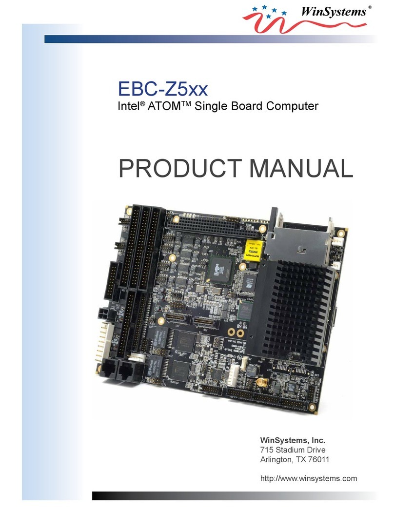
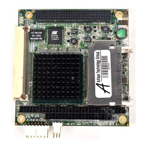
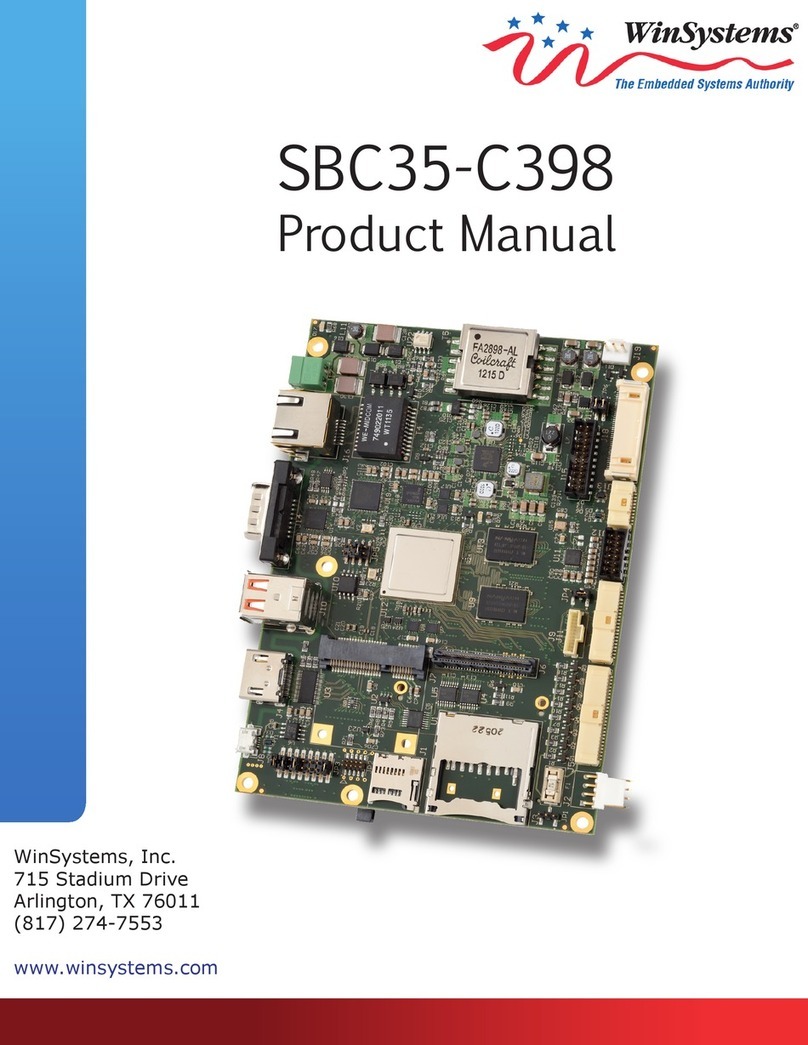
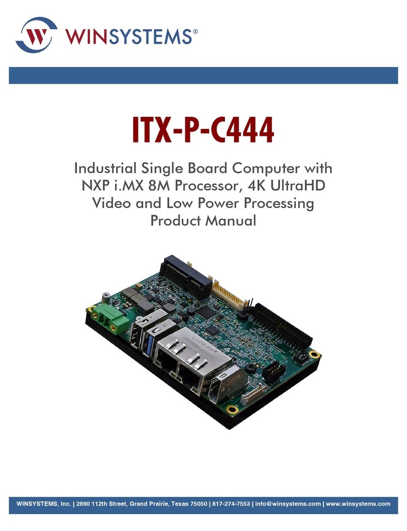
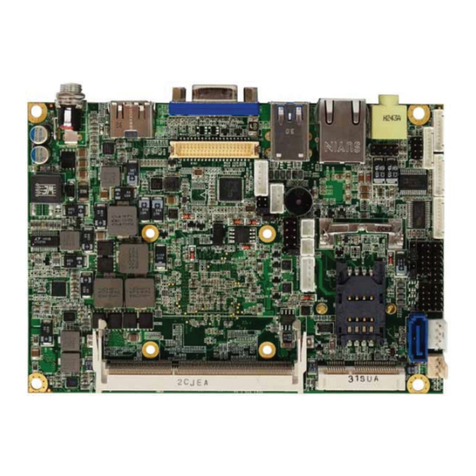
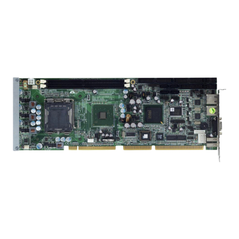
WinSystems LBC- 486Plus User manual

OPERATIONS MANUAL
LBC-486Plus
LBC-586Plus
WinSystems reserves the right to make changes in the circuitry
and specifications at any time without notice.
Copyright 1997 by WinSystems. All Rights Reserved.

REVISION HISTORY
P/N 403-0259-000
ECO Number Date Code Rev Level
ORIGINATED 970422 C
97-36 970602 C1
97-78 970829 C2
97-105 971204 C3
98-01 980107 C4
98-18 980311 C5
98-57 980807 C6
98-86 980817 C7
99-30 990609 D
99-83 991206 E

TABLE OF CONTENTS
SectionParagraph Page
Number Title Number
1General Information
1.1 Features1-1
1.2 General Description 1-1
1.3 Specifications1-2
2LBC-Plus Technical Reference
2.1Introduction 2-1
2.2ALI 1487/1489 Chipset2-1
2.3CPU Speed Selection 2-2
2.4PCI Clock Select2-3
2.5Memory Installation2-3
2.6Interrupt routing2-4
2.7Real Time Clock/Calendar 2-5
2.8 Keyboard Interface 2-5
2.9 Serial Interface 2-6
2.10Parallel Printer Port2-13
2.11Speaker/Sound Interface 2-14
2.12 PC/104 Bus Interface2-14
2.13 Floppy Disk Interface 2-14
2.14 IDE Hard Disk Interface 2-16
2.15Watchdog Timer Configuration 2-16
2.16 Status LED2-17
2.17Battery Select Control2-17
2.18Power/Reset Connection 2-18
2.19 Silicon Disk Configuration2-18
2.20Parallel I/O2-21
2.21VGA Configuration2-24
2.22Ethernet Configuration 2-29
2.23Multi I/O Connector 2-41
2.24Jumper/Connector Summary 2-42
3Award BIOS Configuration
3.1 General Information3-1
3.2 Entering Setup3-1
3.3Setup Main Menu 3-1
3.4Standard CMOS Setup3-2
3.5 BIOS Features Setup3-6
3.6Chipset Features Setup3-10
3.7 Load BIOS Defaults3-13
3.8 Load Setup Defaults 3-13
3.9 Password Setting3-14
3.10IDE HDD Auto Detection3-14

3.11 Save & Exit Setup 3-14
3.12 Exit without Saving 3-14
4LBC-Plus Silicon Disk Reference
4.1 Introduction 4-1
4.2 ROMDISKUsage 4-1
4.3 Bootable RAMDISK/FLASHDISK Usage 4-4
4.4 Non-Bootable RAMDISK Usage 4-5
4.5 Non-Bootable FLASHDISK Usage 4-7
4.6 DiskOnChipUsage 4-7
5WS16C48 Programming Reference
5.1 Introduction 5-1
5.2 Function Definitions 5-1
5.3 SamplePrograms 5-6
APPENDIX A I/O Port Map
APPENDIX B Interrupt Map
APPENDIX C Parts Placement Guide
APPENDIX D LBC-Plus Mechanical Drawing
APPENDIX E WS16C48 I/O Routines and Sample Programs Listings
WARRANTY

1General Information
1.1Features
n486DX4 at 100MHz or 5X86 at 133 MHz
n100% PC-AT Compatible
nUp to 32 Mbytes of user installable FPM or EDO DRAM
nOptional 256K L2 Cache
nSolid State Disk Support of up to 12MB
nPCI High-Resolution VGA controller for CRT or Flat Panel usage
nPCI IDE Controller
nNE2000 Compatible 10BaseT, AUI, Ethernet Controller
nFour 16550 Compatible Serial ports with optional RS422, RS485, J1708 interfaces
nBi-directional Parallel printer port supports EPP and ECP modes
n48 Digital I/O lines with 24 line event sense capability
nDual Floppy Disk interface
n16-Bit PC/104 Expansion Bus
nWatchdog Timer with Power-fail reset
1.2General Description
The LBC-486/586Plus is a small, high-performance, embeddable computer system on a single
board. It integrates a number of popular I/O options including VGA, Ethernet, Solid-State Disk, and
High-Density Parallel I/O. Four PC compatible serial ports are standard, as are the floppy,hard disk,
andparallelprinterinterfaces.TheLBC-Plusispopulated with either a 100 MHz AMD DX4proc essor
or the AMD 5x85 133 MHz processor. Up to 32Mbytes of user installable SIMM memory is sup-
ported. An optional 256KB level two cache is also available. A full 16-bit PC/104 expansion bus is
provided for further expansion to an entire industry of add-on peripherals including sound and speech
modules,SCSIcontrollers,Analog I/O modules, and literally hundreds of other optionsava ilable from
WinSystems and a variety of vendors supporting the PC/104 standard. An onboard silicon disk array
supportsdisksupto2megabytesinsizeandcanutilize SRAM, PEROM or EPROM as the disk media .
Boot capability is provided onboard and a set of utilities and drivers are provided to makethe silicon
disk based system very user friendly. Alternately, the M-Systems DiskOnChip FLASH modules ma y
be populated, supporting disk sizes ranging from 1 Megabyte to 12 Megabytes.
991206 OPERATIONS MANUAL LBC-PlusPage 1- 1
1.3Specifications
1.3.1Electrical
Bus Interface : PC/104 8-Bit or 16-Bit expansion bus
System Clock :Jumper programmable from 4MHz to 50MHz
Interrupts : TTL Level input
VCC :+5V +/- 5% at 2.0A typical with a 133MHz 5X86 processor with 16M DRAM
1.8A typical with a 100MHz DX4 processor and 16M DRAM
VCC1 : +12V +/-5% (Not required. PC/104 Expansion, Flat-Panel, or AUI use only)
VCC2 :-12V +/-5% (Not required. PC/104 Expansion or FLat-Panel use only)
1.3.2Memory
Addressing : 32 Megabyte addressing
BIOS ROM :128K OTPROM
Memory SIMM Socket : 72-pin Fast Page Mode or EDO DRAM in sizes from 1M to 32M
SSD Memory : Two 32-pin JEDEC standard sockets support 4-Mbit SRAM, 4-Mbit PEROM,
4-Mbit EPROM, 8-Mbit EPROM, or one M-Systems 32-Pin DOC (DiskOnChip) module.
1.3.3Mechanical
Dimensions : 5.75 X 8.0 X 0.60 inches (without PC/104 modules or cables)
PC-Board : FR4 Epoxy Glass with 4 signal layers and 2 power planes with screened
component legend, and plated through holes.
Jumpers : 0.025" square posts on 0.10" centers
Connectors : Multi I/O : 50 pin RN type IDH-50LP
COM3/COM4 : 20-pin RN type IDH-20LP
Floppy Disk :34 pin RN type IDH-34-LP
Fixed Disk :40 pin RN type IDH-40-LP
Digital I/O : Two 50 pin RN type IDH-50-LP
10BaseT :RJ45
Page 1- 2OPERATIONS MANUAL LBC-Plus991206
WinSystems- "The Embedded Systems Authority"

Ethernet AUI : 16 pin RN type IDH-16-LP
CRT : 10 pin RN type IDH-10-LP
Flat Panel :50 pin RN type IDH-50-LP
Power/Reset : 8 pin in-line Molex
PC/104 Bus : 64 Pin SAMTEC type ESQ-132-12-G-D
40 Pin SAMTEC type ESQ-120-12-G-D
1.3.4Environmental :
Operating Temperature : -40 °to +70°C
Non-condensing relative humidity : 5% to 95%
991206OPERATIONS MANUAL LBC-PlusPage 1- 3
WinSystems- "The Embedded Systems Authority"

2LBC-PLUS Technical Reference
2.1Introduction
Thissectionofthe manualisintended toprovidesufficientinformationregardingtheconfiguration
and usage of the LBC-Plus board. WinSystems maintains a Technical Support group to help ans wer
questions regarding configuration, usage, or programming of the board. For answers to que stions not
adequately addressed in this manual, contact Technical Support at (817) 274-7553 between 8 AM and
5PM Central Time.
2.2ALI 1487/1489 Chipset
The LBC-Plus utilizes the ALI FINALI-486 Chipset which provides a highly-integrated, high-
performancebackboneforfullPC/ATcompatibility.TheChipsetcontainsthelogicforDRAMandbus
state control as well as the standard complement of 'AT' class peripherals, including :
8 DMA Channels compatible with PC/AT 8237A DMA controllers
15 interrupt inputs compatible with master/slaved 8259 interrupt controllers
Three 8254 compatible timer/counter channels
A PC-AT compatible real time clock/calendar with CMOS RAM
A PCI BUS IDE interface
A PC/AT compatible keyboard interface
These functional units are 100% PC/AT compatible and are supported by the AWARD BIOS and
setup. Users desiringtoaccesstheseinternalperipherals directly should referto any manufacturersge-
neric literature on the equivalent discrete component.
There are a number of internal registers within the Finali-486 chipset that are used by the BIOSfor
control and configuration. Refer to the I/O map in Appendix A for port usage to avoid conf licts when
adding external I/O devices.
991206 OPERATIONS MANUAL LBC-PlusPage 2- 1

2.3CPU Speed Selection
The LBC-Plus uses a Crystal controlled frequency synthesizer to control the CPU clock rate. The
jumper block at J12 allows for the selection of any of 8 CPU base clock frequencies ranging f rom 8
MHz to 100 MHz.
The table below gives all of the possible CPU clock speeds available by jumpering J12.
CPU
SpeedJ12
1-2 J12
3-4 J12
5-6
8 Mhz ONONON
16 MHz ONONOFF
33 MHz ONOFFON
40 MHz ONOFFOFF
50 MHz OFFON ON
66 MHz OFFON OFF
80 MHz OFFOFFON
100 MHzOFF OFF OFF
NOTE : The LBC-Plus board will be jumpered at the factory for the rated speed of the installed
processor. Jumpering J12 to any speed in excess of the rated speed may result in CPU overhea ting,
misoperation, and possible destruction of the CPU. Failures of CPUs which have been operated above
their rated speed or temperature are not covered under the WinSystems standard product warranty.
Page 2- 2OPERATIONS MANUAL LBC-Plus991206
WinSystems- "The Embedded Systems Authority"
1o
2 o
3 o
1o
2 o
3 o
1 o o 2
3 o o 4
5 o o 6
J31
J12
J14
1 2 3
o o o
J36

2.3.1 Clock Multiplier Select
486DX4 and 5X86 processors actually run at a multiple of the base oscillator frequency. T he
jumper block at J36 allows selection of the multiplier as shown here :
2.4PCI Clock Select
The PCI bus clock source must be selected using jumper blocks at J14 and J31. The CPUCLK
source may be selected any time the CPU base frequency is less than or equal to 33MHz. For any CPU
base frequency in excess of 33MHz the CPUCLK/2 selection must be made.
2.5Memory Installation
The LBC-Plus utilizes user installable 72-pin standard SIMMs. SIMM modules should be a
minimum speed of 70nS and X32 architecture is preferred as there is no support for the paritybits pro-
vided by X36 bit modules. A single SIMM socket is provided which can support DRAM sizes from
1MB to 32MB.
Installation is accomplished with power off by angling the SIMM module approximately 30 de -
grees from vertical and inserting the fingers into the connector (It may be necessary to remove any de-
viceinstalledintheU27socket.).TheSIMMmoduleiskeyedslightlyoff-centerandcannotbeinserted
backwards without extreme force. Once the fingers are in the socket, the module is then rotated to the
vertical until the retaining clips snap into place. Removal is the reverse process. Pull th eretainingclips
outward and the SIMM module, once released, should rotate back to an appropriate removal angle.
991206 OPERATIONS MANUAL LBC-PlusPage 2- 3
WinSystems- "The Embedded Systems Authority"
1o
2 o
3 o
1o
2 o
3 o
1o
2 o
3 o
J14J14
J31J31
CPUCLKCPUCLK/2
1o
2 o
3 o
1 2 3
o o o
J36
1 2 3
o o o
J36
3X 2X - 486
4X - 5X86

2.6Interrupt routing
Allinterruptson theLBC-Plusareroutedto theirrespective PC/104buspins. Onboardperiph erals,
serial, parallel, and disk are routed to their typical usage interrupts using the jumper block at J30. This
blockallowsdisconnectingorrerouting of theonboardinterrupts.The layoutfortheJ30headerand the
default jumper settings are shown here.
Page 2- 4OPERATIONS MANUAL LBC-Plus991206
WinSystems- "The Embedded Systems Authority"
1 o o 2
3 o o 4
5 o o 6
7 o o 8
9 o o 10
11 o o 12
13 o o 14
15 o o 16
17 o o 18
19 o o 20
21 o o 22
J30
1 o o 2
3 o o 4
5 o o 6
7 o o 8
9 o o 10
11 o o 12
13 o o 14
15 o o 16
17 o o 18
19 o o 20
21 o o 22
J30
COM4
ENET
COM3
COM4
WS16C48
IDE
LPT
FLOPPY
COM3
COM1
COM2
IRQ9
IRQ10
IEQ11
IRQ12
IRQ15
IRQ14
IRQ7
IRQ6
IRQ5
IRQ4
IRQ3

2.7 Real Time Clock/Calendar
The LBC-Plus contains an onboard Clock/Calendar within the ALI1487 chip. This clock is fully
compatible with the MC146818A used in the original PC-AT computers. This clock has a number of
features including periodic and alarm interrupt capabilities. In addition to the time a nd date keeping
functions,the system configuration iskeptwithinthe CMOS RAMcontainedintheclocksection.This
RAM holds all of the setup information regarding hard and floppy disk types, video type, shadowing,
wait states, etc. Refer to the section on the AWARD BIOS Setup for what is configured via the C MOS
RAM.
ItmaybecomenecessaryatsometimetomaketheCMOSRAMforgetitscurrentconfigurationand
tostartfreshwithfactorydefaults.Thismaybeaccomplishedbyremovingpowerfromtheboa rd.Then
remove the jumper from pins 1-2 on J13 and place on pins 2-3 for 30 seconds. Replace the jumper o n
J13 pins 1-2, power-up, and reconfigure the CMOS settings as desired.
NOTE:J13isthemasterbatteryenablejumper.Removingthejumperremovesbatterypowerfrom
the entire board including the SSD array. Be sure that any data contained in battery backed S RAM is
backed up before removing the battery jumper. J13 must be jumpered 2-3 in the clear position if a bat-
tery is not installed.
2.8Keyboard Interface
The LBC-Plus contains an onboard PC-AT style keyboard controller. Keyboard connection is
made through the Multi-I/O connector at J3. An adapter cable P/N CBL-162-1 is available from W in-
SystemstomakereadyaccesstoallofthedevicesterminatedattheMulti-I/Oconnector.Us ersdesiring
customconnectionsshouldrefertotheMulti-I/Oconnectorpindefinitionsgivenlaterinthismanual.
991206 OPERATIONS MANUAL LBC-PlusPage 2- 5
WinSystems- "The Embedded Systems Authority"
1 2 3
o o o
J13

2.9Serial Interface
The LBC-Plus provides four 16550 compatible RS-232 serial ports at the following addresses :
COM1 3F8H at IRQ 4
COM2 2F8H at IRQ 3
COM3 3E8H* at IRQ 5**
COM4 2E8H* at IRQ 9**
*COM ports 3 and 4 can be enabled or disabledindividually via the jumper block at J23. When J 23
pins 1-2 are jumpered, COM3 is enabled. When J23 pins 3-4 are jumpered, COM4 is enabled.
**The interrupts are not disconnected when COM3 or COM4 are disabled. Use the interrupt rout-
ing block described earlier to disconnect the default interrupts if desired.
Page 2- 6OPERATIONS MANUAL LBC-Plus991206
WinSystems- "The Embedded Systems Authority"
1 2 3
o o o
1 2 3
o o o
U9U6
U5
J11
J9
1 2 3
o o o
1 2 3
o o o
U8U3U4
J10
J8

The two primary serial ports, COM1 and COM2 are configurable for RS-422, RS-485 or J1708,
with the addition of optional driver ICs. The configuration options for each of the supported modes are
shown on the following pages.
COM1 - RS-232
COM2 - RS-232
COM3/COM4 - RS-232
COM3 and COM4 are RS-232 only and are terminated at J2. An adapter cable is available from
WinSystems ( P/N CBL- 173-1), which adapts J2 to two standard DB9M connectors. The pin defini-
tions for J2 are shown here :
991206OPERATIONS MANUAL LBC-PlusPage 2- 7
WinSystems- "The Embedded Systems Authority"
1 2 3
o o o 1 2 3
o o o
U3 - Installed
U4 - Not Installed
U8 - Not Installed
1 o o 6
2 o o 7
3 o o 8
4 o o 9
5 o
J8J10
COM1 DB9
CD
RX Data
TX Data
DTR
GND
DSR
RTS
CTS
RI
1 2 3
o o o 1 2 3
o o o
U5 - Installed
U6 - Not Installed
U9 - Not Installed
J9 J11
COM2 DB9
CD
RX Data
TX Data
DTR
GND
DSR
RTS
CTS
RI
1 o o 6
2 o o 7
3 o o 8
4 o o 9
5 o
1 o o 2
3 o o 4
5 o o 6
7 o o 8
9 o o 10
11 o o 12
13 o o 14
15 o o 16
17 o o 18
19 o o 20
COM3 DCD
COM3 RX
COM3 TX
COM3 DTR
GND
COM4 DCD
COM4 RX
COM4 TX
COM4 DTR
GND
COM3 DSR
COM3 RTS
COM3 CTR
COM3 RI
N/C
COM4 DSR
COM4 RTS
COM4 CTS
COM4 RI
N.C
J2

2.9.1RS-422 Mode Configuration
RS-422 levels are supported on both COM1 and COM2 with the installation of the optional “Chip
Kit”, WinSystems part number CK-75176-2. This kit provides the driver ICs necessary for a single
channelofRS-422. If two channelsofRS-422 are required then two kits will be needed. RS-42 2 is a 4-
wire point-to-point full-duplex interface allowing much longer cable runs than are possible with RS-
232. The differential transmitterandreceiver twisted pairs offer a high degree of noiseimmunity. RS-
422 usually requires the lines be terminated at both ends. This termination can be accomp lished either
onthecableorbyinstallingresistersontheboardinlocationsreservedforthem.Theme thodfordeter-
miningthecorrectresistorvaluesisbeyond the scope of this document but it is recommen ded that trial
values of 100 ohms be used in all three locations at the receiver end. The following illustration shows
thecorrectmode jumpering,driverICinstallation,I/Oconnectorpin definitions,andterminationresis-
tor locations for each of the channels when used in RS-422 mode.
COM1 - RS-422
Page 2- 8OPERATIONS MANUAL LBC-Plus991206
WinSystems- "The Embedded Systems Authority"
1 2 3
o o o 1 2 3
o o o
U3 - Not Installed
U4 - Installed
U8 - Installed
1 o o 6
2 o o 7
3 o o 8
4 o o 9
5 o
J8J10
COM1 DB9
N/C
TX+
TX-
N/C
GND
RX+
RX-
N/C
N/C
VCC
R8
R9
R10
RX+
RX-
RS-422 NOTE : When used in RS-422 mode,
the transmitter must be enabled by setting the RTS
bit in the Modem Control Register (Bit1).

COM2 - RS-422
2.9.2RS-485 Mode Configuration
TheRS-485Multi-dropinterfaceissupportedonbothchannelswiththeinstallationoftheoptional
“ChipKit”,WinSystemspartnumberCK-75176-2.Asinglekitissufficienttoconfigure bothchannels
for RS-485. RS-485 is a 2-wire multi-drop interface where only one station at a time talks (transmits)
while all others listen (receive). RS-485 usually requires the twisted pair be terminated a t each end of
therun.The required termination valuesaredependent upon a number offactorsincluding:lineimped-
ance, line length, etc. A good trial value is 100 ohms in all three resistorlocations. The following illus-
trations show the correct jumpering, driver IC installation, I/O connector pinout, and te rmination
resistor locations for each of the channels when used in RS-485 mode.
991206 OPERATIONS MANUAL LBC-PlusPage 2- 9
WinSystems- "The Embedded Systems Authority"
1 2 3
o o o 1 2 3
o o o
U5 - Not Installed
U6 - Installed
U9 - Installed
1 o o 6
2 o o 7
3 o o 8
4 o o 9
5 o
J9J11
COM2 DB9
N/C
TX+
TX-
N/C
GND
RX+
RX-
N/C
N/C
VCC
R7
R6
R3
RX+
RX-
RS-422 NOTE :When used in RS-422 mode,
the transmitter must be enabled by setting the RTS
bit in the Modem Control Register (Bit1).

COM1 - RS-485
Page 2- 10OPERATIONS MANUAL LBC-Plus991206
WinSystems- "The Embedded Systems Authority"
1 2 3
o o o 1 2 3
o o o
U3 - Not Installed
U4 - Installed
U8 - Not Installed
1 o o 6
2 o o 7
3 o o 8
4 o o 9
5 o
J8J10
COM1 DB9
N/C
TX/RX+
TX/RX-
N/C
GND
N/C
N/C
N/C
N/C
VCC
R8
R9
R10
TX/RX+
TX/RX-
RS-485 NOTE: Because RS-485 uses a single
twisted-pair, all transmitters are connected in paral-
lel. Only one station at a time may transmit or have
its transmitter enabled. The transmitter Enable/Dis-
able is controlled in software using bit 1 in the Mo-
dem Control Register (RTS). When RTS is set, the
transmitteris enabled,andwhen cleared(thenormal
state) the transmitter is disabled and the receiver is
enabled. Note that it is necessary to allow some
minimal settling time after enabling the transmitter
beforetransmittingthefirstcharacter.Likewise,fol-
lowing a transmission, it is necessary to be sure that
all characters have been completely shifted out of
the UART (Check Bit 6 in the Line Status Register)
before disabling the transmitter to avoid chopping
off the last character.

COM2 - RS-485
2.9.3SAE J1708 Configuration
The Society of Automotive Engineers (SAE) J1708 interface is a variation of the RS-485 in terface
whichisusedfor“SerialDataCommunicationsbetweenMicrocomputerSystemsinHeavyDutyVehi-
cle Applications”. It is beyond the scope of this document to go into detail on the J1708 spe cification.
The LBC-Plus may be user configured for J1708 by the addition of the CK-75176-2 “Chip Kit”. One
“ChipKit”issufficienttoconfigurebothchannelsforJ1708. Theillustrationsthatfoll owshowthecor-
rectjumpering,driverICinstallation,I/Oconnectorpindefinitions,andtheterminationnetworkdetails
for each of the channels when used in J1708 mode.
991206 OPERATIONS MANUAL LBC-PlusPage 2- 11
WinSystems- "The Embedded Systems Authority"
1 2 3
o o o 1 2 3
o o o
U5 - Not Installed
U6 - Installed
U9 - Not Installed
1 o o 6
2 o o 7
3 o o 8
4 o o 9
5 o
J9J11
COM2 DB9
N/C
TX/RX+
TX/RX-
N/C
GND
N/C
N/C
N/C
N/C
VCC
R14
R15
R16
TX/RX+
TX/RX-
RS-485 NOTE: Because RS-485 uses a single
twisted-pair, all transmitters are connected in paral-
lel. Only one station at a time may transmit or have
its transmitter enabled. The transmitter Enable/Dis-
able is controlled in software using bit 1 in the Mo-
dem Control Register (RTS). When RTS is set, the
transmitteris enabled,andwhen cleared(thenormal
state) the transmitter is disabled and the receiver is
enabled. Note that it is necessary to allow some
minimal settling time after enabling the transmitter
beforetransmittingthefirstcharacter.Likewise,fol-
lowing a transmission, it is necessary to be sure that
all characters have been completely shifted out of
the UART (Check Bit 6 in the Line Status Register)
before disabling the transmitter to avoid chopping
off the last character.

COM1 - J1708
COM2 - J1708
Page 2- 12OPERATIONS MANUAL LBC-Plus 991206
WinSystems- "The Embedded Systems Authority"
1 2 3
o o o 1 2 3
o o o
U3 - Not Installed
U4 - Installed
U8 - Not Installed
1 o o 6
2 o o 7
3 o o 8
4 o o 9
5 o
J8J10
COM1 DB9
N/C
TX/RX+
TX/RX-
N/C
GND
N/C
N/C
N/C
N/C
VCC
R11
4.7K
R12
Absent
R13
4.7K
TX/RX+
TX/RX-
R1 470 OHM
R2 470 OHM
C1 .0022 ufd
C2 .0022 ufd
1 2 3
o o o 1 2 3
o o o
U5 - Not Installed
U6 - Installed
U9 - Not Installed
1 o o 6
2 o o 7
3 o o 8
4 o o 9
5 o
J9J11
COM2 DB9
N/C
TX/RX+
TX/RX-
N/C
GND
N/C
N/C
N/C
N/C
VCC
R14
4.7K
R15
Absent
R16
4.7K
TX/RX+
TX/RX-
R5 470 OHM
R4 470 OHM
C4 .0022 ufd
C3 .0022 ufd

2.10Parallel Printer Port
The LBC-Plus supports a fully bi-directional parallel printer port capable of EPP and ECP op era-
tions.Theparallel portismapped at278Hand isterminatedattheMulti-I/OconnectorJ3.Thepindefi-
nitions for the parallel port DB25 connector when using the CBL-162-1 cable are shown below:
2.10.1 Parallel Port Mode Selection
The parallel port mode is selected via the jumper block at J6 per the following table :
J6
Jumpering
SPP Mode EPP Mode ECP Mode EPP/ECP Mode
3-5
4-63-5
2-41-3
4-61-3
2-4
991206OPERATIONS MANUAL LBC-PlusPage 2- 13
WinSystems- "The Embedded Systems Authority"
1 2
o o
o o
3 4
1 2
o o
o o
3 4
1 o o 2
3 o o 4
5 o o 6
J24
J21
J6
1 o o 14
2 o o15
3 o o16
4 o o17
5 o o18
6 o o 19
7 o o 20
8 o o 21
9 o o 22
10 o o23
11 o o24
12 o o25
13 o
STROBE
PD0
PD1
PD2
PD3
PD4
PD5
PD6
PD7
ACK
BUSY
PE
SLCT
AUTOFD
ERROR
INIT
SLIN
GND
GND
GND
GND
GND
GND
GND
GND
This manual suits for next models
1
Table of contents
Other WinSystems Single Board Computer manuals

WinSystems
WinSystems ITX-P-C444 User manual

WinSystems
WinSystems PPM-C412 User manual

WinSystems
WinSystems SYS-405 User manual

WinSystems
WinSystems SBC35-C398 User manual

WinSystems
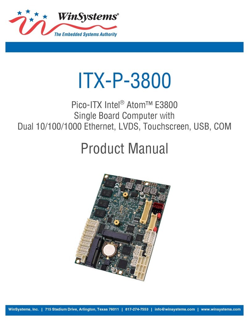
WinSystems ITX-P-3800 User manual

WinSystems
WinSystems EPX-C414 User manual

WinSystems
WinSystems PPM-LX800-G User manual

WinSystems
WinSystems EBC-Z5xx User manual