AG-Stomp
3
SPECIFICATIONS
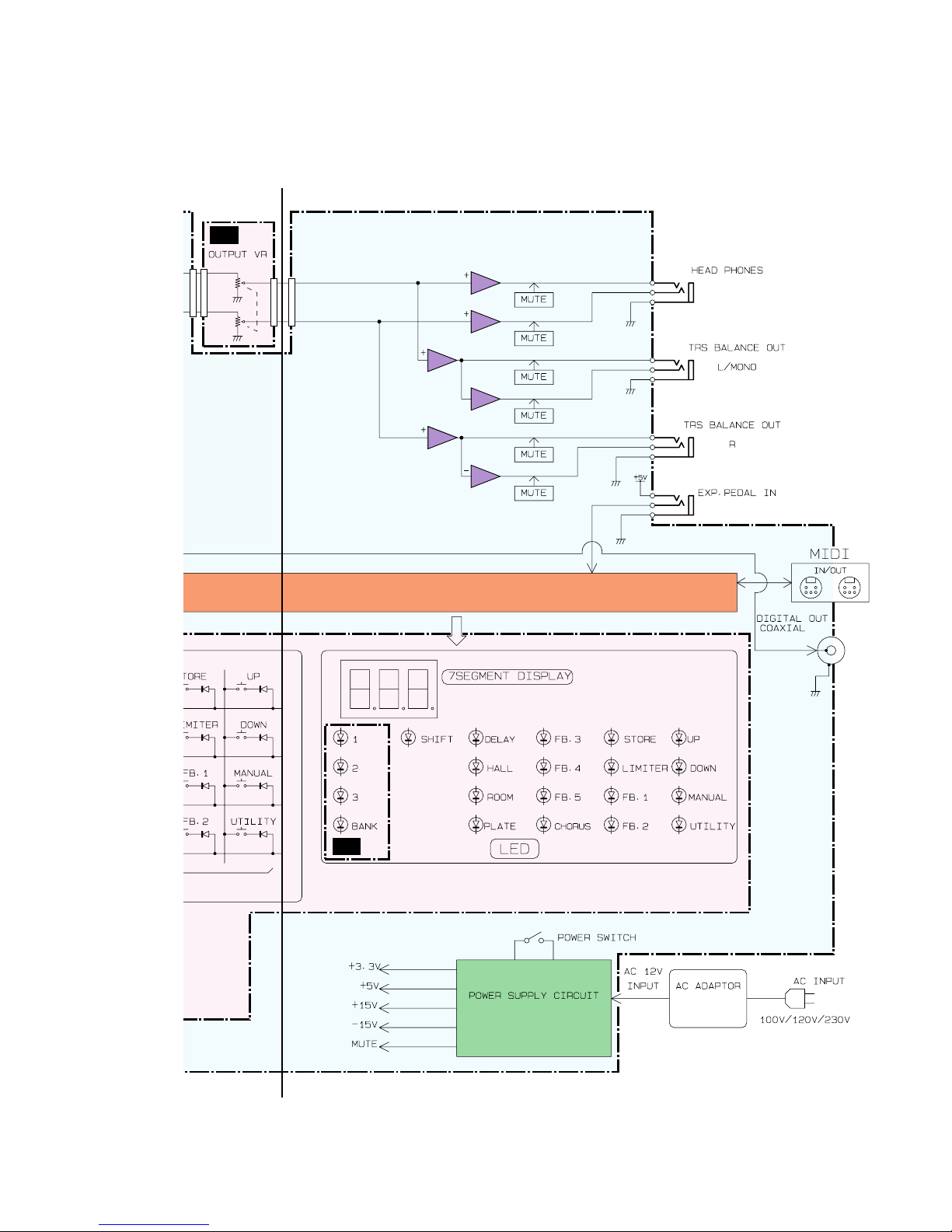
Digital Section
• Full Digital Signal Processing
• Mic Simulator: 8 Types
• Feedback Reduction: 5-band
• Digital Effects
• Limiter
• Digital Chorus, Digital Delay
• Hall Reverb, Room Reverb, Plate Reverb
• External Controller Function (EXP Pedal/MIDI): 8 Controllers/
Parameters
• Tuner Function (Chromatic, Auto)
MIDI Functions
Receive:Program Change (Program Change Table can be cre-
ated), Control Change, Bulk In
Transmit: Program Change, Control Change, Bulk Out, Merge
Out
Guitar Power Supply
9V power can be supplied via aTRS phone cable to a guitar’s
built-in pre-amplifier, etc. that consumes less than 10mA of
power, and uses a monaural output.
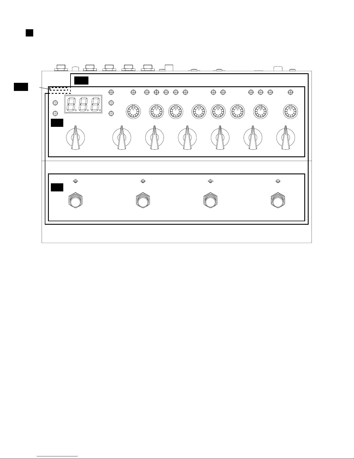
Controller/Switch
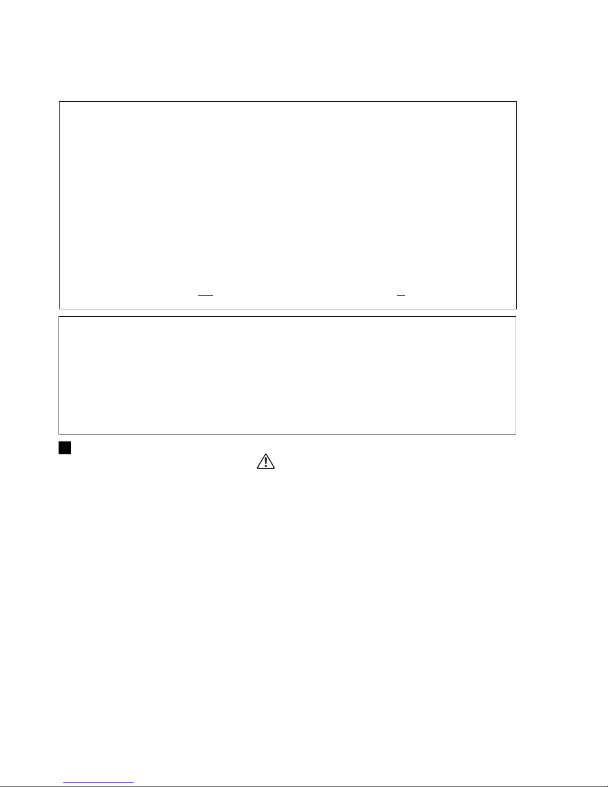
Top Panel
Push Switch x17
UP, DOWN, MANUAL, UTILITY, STORE, LIMITER, FEED
BACK REDUCTION 1-5, CHORUS, DELAY, HALL, ROOM,
PLATE, SHIFT
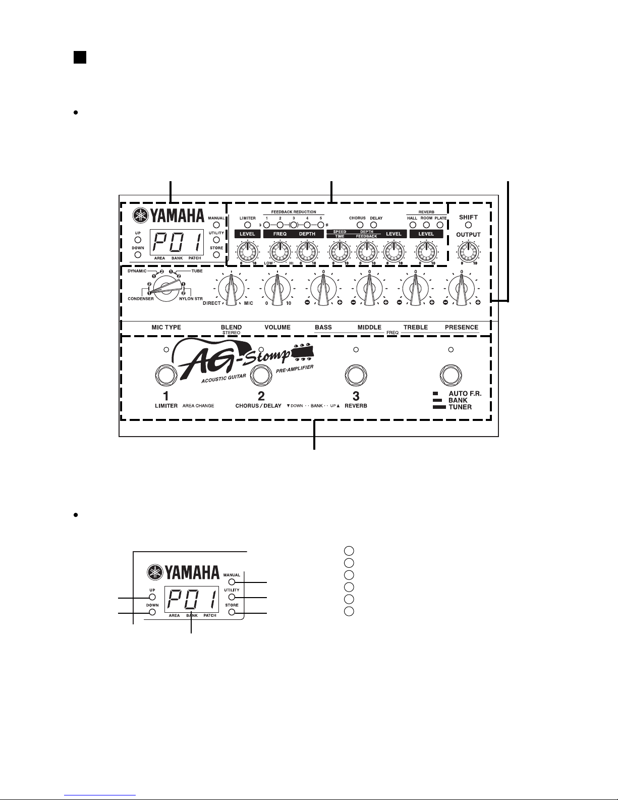
Knob x15
MICTYPE, BLEND, VOLUME, BASS, MIDDLE,TREBLE,
PRESENCE, LIMITER LEVEL, FEEDBACK REDUCTION
FREQ, FEEDBACK REDUCTION DEPTH, CHORUS
SPEED/DELAY TIME, CHORUS DEPTH/DELAY FEED
BACK,CHORUS LEVEL/DELAY LEVEL,REVERB LEVEL,
OUTPUT
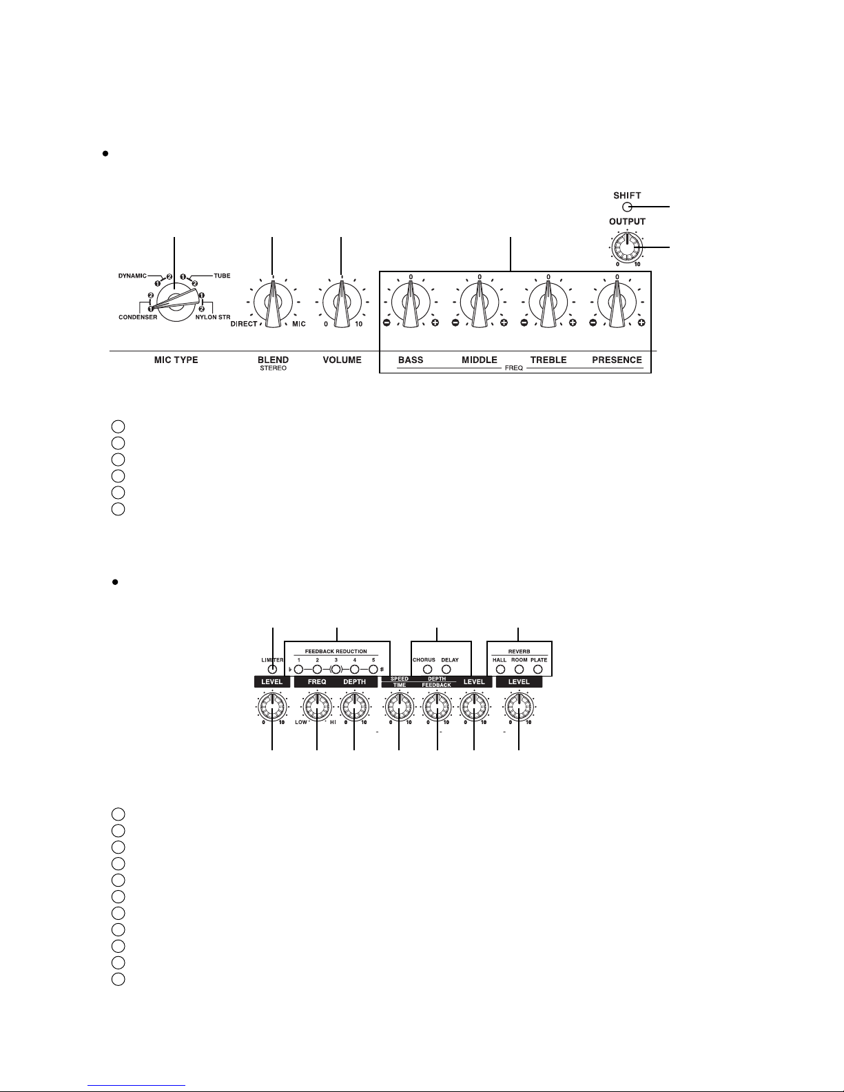
Footswitch x4
1, 2, 3 BANK
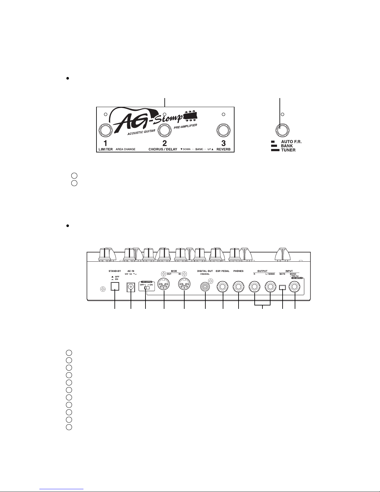
Rear Panel
STAND-BY ON/OFF, MUTE, +9V SUPPLY ON/OFF
Display
7 Segment LED (3 digit) x1
Push Switch LED x17
Footswitch LED x4
Connections
INPUT:Standard Stereo Phone Jack
OUTPUT L/MONO, R: Standard Stereo Phone Jack (TRS Bal
anced)
PHONES: Standard Stereo Phone Jack
EXP. PEDAL: Standard Stereo Phone Jack
DIGITAL OUT: COAXIAL
MIDI IN, MIDI OUT:5-pin DIN
A/D Converter
20 bit
D/A Converter
20 bit
Sampling Frequency
44.1kHz
Memory Allocations
Preset: 30
User: 30
Input Level/Impedance
(When using pre-amp bypass)
INPUT: -17dBm/1MΩ
Output Level/Impedance
OUTPUT L/MONO: Balance +4dBm/600Ω
OUTPUT R: Balance +4dBm/600Ω
PHONES: 0dBm/47Ω
Power
Exclusive Power Adaptor (AC-10)
AC Output:AC12V, 1A
Power Consumption
15W
Dimensions
280(W)x70(H)x184(D)mm (11.0"x2.8"x7.2")
Weight
2.2 kg (4lbs. 4oz.)
Accessories
Power Adaptor (AC-10)
TRS Phone Cable for Guitar Power Supply (3m)
TRS-XLR Converter Cable (x2)
Dummy Battery
Owner’s Manual