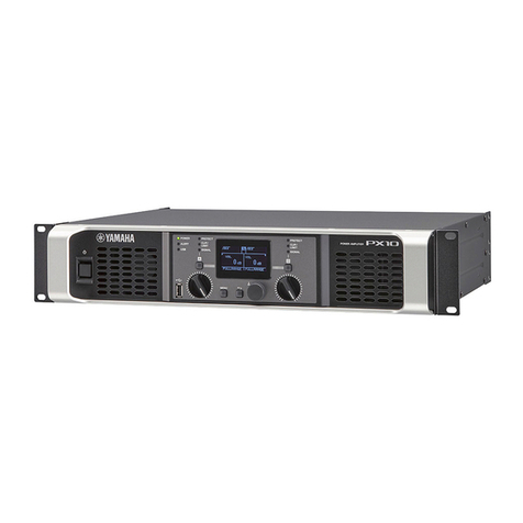
Yamaha PX10 User manual

SERVICE MANUAL
HAMAMATSU, JAPAN
SERVICE MANUAL
SPECIFICATIONS(総合仕様)....................................3
PANEL LAYOUT(パネルレイアウト)..............................6
DIMENSIONS(寸法図)...............................................7
JACK AND PLUG LIST(端子とプラグ一覧)..................8
CIRCUIT BOARD LAYOUT(ユニットレイアウト)..............9
DISASSEMBLY PROCEDURE(分解手順)............... 10
LSI PIN DESCRIPTION(LSI端子機能表)................. 18
CIRCUIT BOARDS(シート基板図).............................21
INSPECTION(検査)............................................32/61
MEASUREMENT(測定)......................................53/82
UPDATING FIRMWARE(ファームウェアのアップデート)
...60/89
DEVICE BACKUP(デバイスバックアップ)..................90
CONTENTS(目次)
INITIALIZING THE PX AMPLIFIER
(PXアンプの初期化)..................................................92
FUNCTION LIST(機能一覧).......................................94
MESSAGE LIST(メッセージリスト)............................96/97
START-UP SEQUENCE(起動シーケンス)........... 99/100
ENDING SEQUENCE(終了シーケンス).............101/102
PARTS LIST
BLOCK DIAGRAM(ブロックダイアグラム )
LEVEL DIAGRAM(レベルダイアグラム)
WIRING(結線図)
CIRCUIT DIAGRAM(回路図)
Copyright (c) Yamaha Corporation. All rights reserved. PDF ’16.10
PA 012180
POWER AMPLIFIER
PX10
PX8
PX5
PX3

2
PX10/PX8/PX5/PX3
WARNING: This product contains chemicals known to the State of California to cause cancer, or birth defects or other reproductive harm.
DO NOT PLACE SOLDER, ELECTRICAL/ELECTRONIC OR PLASTIC COMPONENTS IN YOUR MOUTH FOR ANY REASON WHAT SO EVER!
Avoid prolonged, unprotected contact between solder and your skin! When soldering, do not inhale solder fumes or expose eyes to solder/ flux
vapor!
If you come in contact with solder or components located inside the enclosure of this product, wash your hands before handling food.
IMPORTANT NOTICE
This manual has been provided for the use of authorized Yamaha Retailers and their service personnel. It has been assumed that basic ser-
vice procedures inherent to the industry, and more specifically Yamaha Products, are already known and understood by the users, and have
therefore not been restated.
WARNING : Failure to follow appropriate service and safety procedures when servicing this product may result in personal injury, de-
struction of expensive components and failure of the product to perform as specified. For these reasons, we advise all
Yamaha product owners that all service required should be performed by an authorized Yamaha Retailer or the appointed
service representative.
IMPORTANT : This presentation or sale of this manual to any individual or firm does not constitute authorization certification, recog-
nition of any applicable technical capabilities, or establish a principal-agent relationship of any form.
The data provided is believed to be accurate and applicable to the unit(s) indicated on the cover. The research engineering, and service
departments of Yamaha are continually striving to improve Yamaha products. Modifications are, therefore, inevitable and changes in
specification are subject to change without notice or obligation to retrofit. Should any discrepancy appear to exist, please contact the
distributor’s Service Division.
WARNING : Static discharges can destroy expensive components. Discharge any static electricity your body may have accumulated by
grounding yourself to the ground bus in the unit (heavy gauge black wires connect to this bus.)
IMPORTANT : Turn the unit OFF during disassembly and parts replacement. Recheck all work before you apply power to the unit.
IMPORTANT NOTICE FOR THE UNITED KINGDOM
Connecting the Plug and Cord
WARNING: THIS APPARATUS MUST BE EARTHED IMPORTANT. The wires in this mains lead are coloured in accordance with
the following code:
GREEN-AND-YELLOW : EARTH
BLUE : NEUTRAL
BROWN : LIVE
As the colours of the wires in the mains lead of this apparatus may not correspond with the coloured markings identifying the
terminals in your plug proceed as follows:
The wire which is coloured GREEN-and-YELLOW must be connected to the terminal in the plug which is marked by the letter E
or by the safety earth symbol or colored GREEN or GREEN-and-YELLOW.
The wire which is coloured BLUE must be connected to the terminal which is marked with the letter N or coloured BLACK.
The wire which is coloured BROWN must be connected to the terminal which is marked with the letter L or coloured RED.
WARNING
WARNING
Components having special characteristics are marked and must be replaced with parts having specification equal to those
originally installed.
Please keep the USB cap out of reach of children, to keep them from accidentally swallowing it.
This mark indicates a dangerous electrically live terminal. When connecting an external wire to
this terminal, it is necessary either to have “a person who have received appropriate guidance on
handling” make the connection or to use leads or a cord that have been manufactured in such a
way that the connection can be made simply and without problem.
印の部品は、安全を維持するために重要な部品です。交換する場合は、安全のために必ず指定の部品をご使用ください。
USBキャップは、子供が誤って飲み込まないように、子供の手の届かないところに保管してください。
マークは、危険活電部であることを示します。この端子への外部からの配線接続は、適正な取扱指導を
受けた者が行なうか、問題なく容易に接続できるように製作されたリ−ド線、またはコードを使用する
必要があります。
(3 wires)

3
PX10/PX8/PX5/PX3
SPECIFICATIONS(総合仕様)
PX10 PX8 PX5 PX3
Output Power
(出力) 120 V 60 Hz, 220 V-240 V 50 Hz/60 Hz
1 kHz, non-clip, 20 msec burst,
both channels driven
8Ω 1000 W × 2 800 W × 2 500 W × 2 300 W × 2
4Ω 1200 W × 2 1050 W × 2 800 W × 2 500 W × 2
2Ω 700 W × 2 600 W × 2 500 W × 2 300 W × 2
1 kHz, non-clip, 20 msec burst 8Ω/Power Boost Mode — — 800 W × 1 600 W × 1
4Ω/Power Boost Mode — — 1400 W × 1 1000 W × 1
Output Power
(出力) 100 V 50 Hz/60 Hz
1 kHz, non-clip, 20 msec burst,
both channels driven
8Ω 1000 W × 2 800 W × 2 500 W × 2 300 W × 2
4Ω 1200 W × 2 1050 W × 2 800 W × 2 500 W × 2
2Ω 700 W × 2 600 W × 2 500 W × 2 300 W × 2
1 kHz, non-clip, 20 msec burst 8Ω/Power Boost Mode — — 800 W × 1 600 W × 1
4Ω/Power Boost Mode — — 1200 W × 1 1000 W × 1
Amplifier Type (Output Circuitry)
(増幅方式(出力回路))Class D, balanced output circuit (BTL)
(ClassD、バランス出力回路(BTL))
THD+N
(全高調波歪率) 1 kHz, 10 W 0.1%
1 kHz, half power 0.3%
Frequency Response
(周波数特性)
1 W, 8Ω, 20 Hz to 20 kHz ±1.0 dB
Crosstalk
(クロストーク)
Half power, 8Ω, 1 kHz, vol. max., input 150Ω shunt
≦-60 dB
S/N Ratio
(S/N 比)
A-weighted, 8Ω, gain setting = +14 dBu 101 dB
101 dB 100 dB 100 dB
Voltage Gain/Sensitivity
(電圧利得 / 感度)
Gain setting: 32 dB 32.0 dB/+9.3 dBu 32.0 dB/+8.3 dBu 32.0 dB/+6.3 dBu 32.0 dB/+4.1 dBu
8Ω, volume max. Gain setting: 26 dB 26.0 dB/+15.3 dBu 26.0 dB/+14.3 dBu 26.0 dB/+12.3 dBu 26.0 dB/+10.1 dBu
Gain setting: +4 dBu 37.3 dB/+4 dBu 36.3 dB/+4 dBu 34.3 dB/+4 dBu 32.1 dB/+4 dBu
Gain setting: +14 dBu 27.3 dB/+14 dBu 26.3 dB/+14 dBu 24.3 dB/+14 dBu 22.1 dB/+14 dBu
Gain setting: 32 dB — — 34.0 dB/+6.3 dBu 35.0 dB/+4.1 dBu
8Ω, volume max.,
Power Boost mode
Gain setting: 26 dB — — 28.0 dB/+12.3 dBu 29.0 dB/+10.1 dBu
Gain setting: +4 dBu — — 36.3 dB/+4 dBu 35.1 dB/+4 dBu
Gain setting: +14 dBu — — 26.3 dB/+14 dBu 25.1 dB/+14 dBu
Load Protection
(負荷保護)
POWER switch on/off Output mute
Output voltage protection Over voltage limiter, user configurable by wattage and speaker preset
DC-fault Power supply shutdown (NOT restored automatically)
Amplifier Protection
(アンプ保護)
Thermal Output limiter (Restored automatically) →Output mute (Restored automatically)
Over current Output mute (Restored automatically)
Over voltage Output limiter (Restored automatically)
Integrated Power Limit Output limiter (Restored automatically)
Power Supply Protection
(電源保護)
Thermal Output limiter (Restored automatically) →Power supply shutdown
Over voltage Power supply shutdown
Over current Power supply shutdown
Cooling
(冷却)
16 step variable speed fan × 2, front to rear airflow
Maximum Input Voltage
(最大入力電圧) +24 dBu
Input Impedance
(入力インピーダンス)
20 kΩ (Balance), 10 kΩ (Unbalance)
Sampling Frequency
(サンプリング周波数)
48 kHz
A/D, D/A Converters
(AD、DA コンバーター)
AD: 24-bit linear, 128 times over sampling
DA: 24-bit linear, 128 times over sampling
Signal Processing
(信号処理)
Input summing
D-CONTOUR: FOH/MAIN, MONITOR, OFF
Delay: 0–74msec
HPF/LPF: cutoff frequency 20 Hz–20 kHz with polarity control
Speaker processor: 6 band PEQ + Limiter + Delay
Latency
(遅延)
Analog input to speakers 1.5 msec
User Amplifier Preset
(ユーザーアンププリセット)
8 user amplifier presets
Factory Speaker Preset
(出荷時スピーカープリセット)
Speaker presets for Yamaha passive speakers
Connectors
(端子)
Analog input XLR-3-31 × 2, 1/4" PHONE(TRS) × 2
Speakers Neutrik speakON NL4 × 2, binding post × 2 pairs, 1/4" PHONE(TS) × 2
AC IN AC inlet × 1 with AC cord clamp
USB
USB 2.0 Standard-A connector (female) for save/load, speaker preset update, firmware update with USB flash drive
Controls
(操作子)
Front Panel POWER switch, 31 step volume knob × 2, rotary encoder and switches for GUI control
Operation lock feature (Full lock or Lock except volume and mute)
Display 128 × 64 pixel, mono color with brightness adjustment
Auto display off feature
Indicators
(インジケーター)
POWER × 1 (green), ALERT × 1 (red), USB × 1 (green), PROTECT × 2 (red), CLIP/LIMIT × 2 (red),
SIGNAL × 2 (green),Auto LED off feature
AC Power Requirement
(電源条件)
Depending on area of purchase; 100 V 50 Hz/60 Hz, 120 V 60 Hz, 220 V-240 V 50 Hz/60 Hz *1
Power Consumption
(消費電力)
1/8 MAX power, 4Ω, Pink noise at all channels
310 W 280 W 230 W 160 W
Idle, 4Ω 60 W 60 W 55 W 55 W
Operating Temperature
(使用温度)
0°C to +40°C
Storage Temperature
(保存温度)
-20°C to +60°C
Dimensions (W × H × D)
(外形寸法)
480 × 88 × 388 mm (18.90 × 3.46 × 15.28 inch)
Net Weight
(質量)
7.4 kg (16.31 lbs) 7.2 kg (15.87 lbs) 6.9 kg (15.21 lbs) 6.9 kg (15.21 lbs)
Included accessories
(付属品)
• AC power cord • Owner’s Manual • Technical Specifications (English) • AC plug clamp • USB cap
(•電源コード•3芯−2芯変換プラグ•取扱説明書•TechnicalSpecifications(スペックシート、英文)
•電源コード誤脱防止クランプ•USBキャップ)
*1 Device operation has been confirmed within ±10% of the rated power supply voltage.
(定格電源電圧の± 10% の電圧で動作することを確認しています。)
4
PX10/PX8/PX5/PX3
•Current draw and thermal dissipation
(消費電流と熱放散)
Testsignal:Pinknoise(bandwidthlimitedfrom22Hzto22kHz),1Btu=1,055.06J=0.252kcal,(W)×0.86=kcal
(テスト信号:ピンクノイズ(22Hz から 22kHz に帯域制限 )、1BTU=1,055.06J=0.252kcal、1W=0.86kcal)
●PX10
100 V/50 Hz
Line current (A)
(線電流)
Watt (W)
(電力)
Thermal dissipation
(熱放散)
100 V Power consumption (In)
(消費電力)
Power consumption (Out)
(消費電力)
Watts dissipated
(放散電力) Btu/h kcal/h
Idle
(アイドル) 0.8 57 0 57 195 49
1/8 out 8Ω/ch 2.6 213 125 88 300 76
4Ω/ch 3.1 261 150 111 379 95
1/3 out 8Ω/ch 5.6 472 333 139 474 120
4Ω/ch 7.2 608 400 208 710 179
110 V-120 V/60 Hz
Line current (A)
(線電流)
Watt (W)
(電力)
Thermal dissipation
(熱放散)
120 V Power consumption (In)
(消費電力)
Power consumption (Out)
(消費電力)
Watts dissipated
(放散電力) Btu/h kcal/h
Idle
(アイドル) 0.7 60 0 60 205 52
1/8 out 8Ω/ch 2.2 213 125 88 300 76
4Ω/ch 2.7 263 150 113 386 97
1/3 out 8Ω/ch 4.6 466 333 133 454 114
4Ω/ch 5.9 597 400 197 672 169
220 V-240 V/50 Hz
Line current (A)
(線電流)
Watt (W)
(電力)
Thermal dissipation
(熱放散)
230 V Power consumption (In)
(消費電力)
Power consumption (Out)
(消費電力)
Watts dissipated
(放散電力) Btu/h kcal/h
Idle
(アイドル) 0.5 62 0 62 212 53
1/8 out 8Ω/ch 1.4 219 125 94 321 81
4Ω/ch 1.6 271 150 121 413 104
1/3 out 8Ω/ch 2.7 471 333 138 471 119
4Ω/ch 3.3 602 400 202 689 174
●PX8
100 V/50 Hz
Line current (A)
(線電流)
Watt (W)
(電力)
Thermal dissipation
(熱放散)
100 V Power consumption (In)
(消費電力)
Power consumption (Out)
(消費電力)
Watts dissipated
(放散電力) Btu/h kcal/h
Idle
(アイドル) 0.8 57 0 57 195 49
1/8 out 8Ω/ch 2.2 178 100 78 266 67
4Ω/ch 2.9 237 131 106 362 91
1/3 out 8Ω/ch 4.6 386 267 119 406 102
4Ω/ch 6.4 543 350 193 659 166
110 V-120 V/60 Hz
Line current (A)
(線電流)
Watt (W)
(電力)
Thermal dissipation
(熱放散)
120 V Power consumption (In)
(消費電力)
Power consumption (Out)
(消費電力)
Watts dissipated
(放散電力) Btu/h kcal/h
Idle
(アイドル) 0.7 60 0 60 205 52
1/8 out 8Ω/ch 1.9 182 100 82 280 71
4Ω/ch 2.5 237 131 106 362 91
1/3 out 8Ω/ch 3.8 385 267 118 403 101
4Ω/ch 5.4 542 350 192 655 165
220 V-240 V/50 Hz
Line current (A)
(線電流)
Watt (W)
(電力)
Thermal dissipation
(熱放散)
230 V Power consumption (In)
(消費電力)
Power consumption (Out)
(消費電力)
Watts dissipated
(放散電力) Btu/h kcal/h
Idle
(アイドル) 0.5 62 0 62 212 53
1/8 out 8Ω/ch 1.2 184 100 84 287 72
4Ω/ch 1.5 242 131 111 379 95
1/3 out 8Ω/ch 2.2 385 267 118 403 101
4Ω/ch 3.0 544 350 194 662 167

5
PX10/PX8/PX5/PX3
●PX5
100 V/50 Hz
Line current (A)
(線電流)
Watt (W)
(電力)
Thermal dissipation
(熱放散)
100 V Power consumption (In)
(消費電力)
Power consumption (Out)
(消費電力)
Watts dissipated
(放散電力) Btu/h kcal/h
Idle
(アイドル) 0.8 46 0 46 157 40
1/8 out 8Ω/ch 1.9 122 63 59 201 51
4Ω/ch 2.7 189 100 89 304 77
1/3 out 8Ω/ch 3.6 253 167 86 293 74
4Ω/ch 5.6 424 267 157 536 135
110 V-120 V/60 Hz
Line current (A)
(線電流)
Watt (W)
(電力)
Thermal dissipation
(熱放散)
120 V Power consumption (In)
(消費電力)
Power consumption (Out)
(消費電力)
Watts dissipated
(放散電力) Btu/h kcal/h
Idle
(アイドル) 0.8 54 0 54 184 46
1/8 out 8Ω/ch 1.7 130 63 67 229 58
4Ω/ch 2.4 196 100 96 328 83
1/3 out 8Ω/ch 3.1 259 167 92 314 79
4Ω/ch 4.8 428 267 161 549 138
220 V-240 V/50 Hz
Line current (A)
(線電流)
Watt (W)
(電力)
Thermal dissipation
(熱放散)
230 V Power consumption (In)
(消費電力)
Power consumption (Out)
(消費電力)
Watts dissipated
(放散電力) Btu/h kcal/h
Idle
(アイドル) 0.5 57 0 57 195 49
1/8 out 8Ω/ch 1.0 130 63 67 229 58
4Ω/ch 1.4 197 100 97 331 83
1/3 out 8Ω/ch 1.9 259 167 92 341 79
4Ω/ch 2.9 434 267 167 570 144
●PX3
100 V/50 Hz
Line current (A)
(線電流)
Watt (W)
(電力)
Thermal dissipation
(熱放散)
100 V Power consumption (In)
(消費電力)
Power consumption (Out)
(消費電力)
Watts dissipated
(放散電力) Btu/h kcal/h
Idle
(アイドル) 0.8 46 0 46 157 40
1/8 out 8Ω/ch 1.5 94 38 56 191 48
4Ω/ch 2.0 137 63 74 253 64
1/3 out 8Ω/ch 2.6 174 100 74 253 64
4Ω/ch 3.9 285 167 118 403 101
110 V-120 V/60 Hz
Line current (A)
(線電流)
Watt (W)
(電力)
Thermal dissipation
(熱放散)
120 V Power consumption (In)
(消費電力)
Power consumption (Out)
(消費電力)
Watts dissipated
(放散電力) Btu/h kcal/h
Idle
(アイドル) 0.8 54 0 54 184 46
1/8 out 8Ω/ch 1.3 100 38 62 212 53
4Ω/ch 1.8 140 63 77 263 66
1/3 out 8Ω/ch 2.3 183 100 83 283 71
4Ω/ch 3.4 291 167 124 423 107
220 V-240 V/50 Hz
Line current (A)
(線電流)
Watt (W)
(電力)
Thermal dissipation
(熱放散)
230 V Power consumption (In)
(消費電力)
Power consumption (Out)
(消費電力)
Watts dissipated
(放散電力) Btu/h kcal/h
Idle
(アイドル) 0.5 57 0 57 195 49
1/8 out 8Ω/ch 0.8 101 38 63 215 54
4Ω/ch 1.1 142 63 79 270 68
1/3 out 8Ω/ch 1.4 181 100 81 276 70
4Ω/ch 2.1 293 167 126 430 108

6
PX10/PX8/PX5/PX3
q電源ボタン
w[POWER]インジケーター
e[ALERT]インジケーター
r[USB]インジケーター
t[CLIP/LIMIT]インジケーター
y[SIGNAL]インジケーター
u[PROTECT]インジケーター
iディスプレイ
o[MENU]キー
!0 [ ](バック)キー
!1 メインノブ
!2 [A]/[B]キー
!3 [USB] 端子
!4 ボリュームノブ
!5 吸気口
PANEL LAYOUT(パネルレイアウト)
qPower button
w[POWER] indicator
e[ALERT] indicator
r[USB] indicator
t[CLIP/LIMIT] indicators
y[SIGNAL] indicators
u[PROTECT] indicators
iDisplay
o[MENU] key
!0 [ ] (Back) key
!1 Main knob
!2 [A]/[B] keys
!3 [USB] terminal
!4 Volume knobs
!5 Intake ports
• Front Panel(フロントパネル)

7
PX10/PX8/PX5/PX3
!6 [INPUT]A/B端子
!7 [SPEAKERS]A/B端子
!8 ACIN端子
!9排気口
!6 [INPUT] A/B connectors
!7 [SPEAKERS] A/B terminals
!8 AC IN connector
!9 Exhaust ports
• Rear Panel(リアパネル)
DIMENSIONS(寸法図)
430
480
361 (Mounting Surface to Rear End)
388
24.5
2.5
29
unit(単位): mm
88

8
PX10/PX8/PX5/PX3
JACK AND PLUG LIST(端子とプラグ一覧)
• XLR jack
(XLR端子)
XLR type 3-31 jack.
(XLR型3-31タイプの端子です。)
The polarity is shown below (IEC60268).
(極性は次のとおりです(IEC60268)。)
• Binding post connector
(バインディングポスト端子)
• Without plugs
(プラグなしの場合)
Remove about 15 mm of insulation from the end of each
speaker cable, pass the bare wire through the holes in the
appropriate speaker terminals, and tighten the terminals to
securely clamp the wires. Make sure that the bare wire ends do
not jut out from the terminals and touch the chassis.
(スピーカーケーブルの先端の被覆を15mm外し、端子の穴に通
して締め付けます。このとき、芯線がシャーシに当たらないよう
にしてください。)
• Y-plugs
(Y型プラグの場合)
From above, insert the Y-plugs all the way into the opening, and
tighten the terminals.
(Y型プラグを上から奥まで差し込み、締め付けます。)
• Phone jack
(フォーン端子)
Balanced TRS phone jack.
(バランス型のTRSフォーン端子です。)
The polarity of the connections is shown below.
(接続する極性は次のとおりです。)
• SpeakON connector
(スピコン端子)
Insert the SpeakON cable plug (Neutrik NL4) into the
connector, and turn it to the right to lock it.
(スピコンケーブルプラグ(NeutrikNL4)を差し込み、
右に回してロックします。)
21
3
Ground(グラウンド)
Cold(コールド)
Hot(ホット)
Ring (cold)(リング(コールド))
Tip (hot)(チップ(ホット))Sleeve (ground)
(スリーブ(グラウンド))
15 mm
0.25"
(6.3 mm)
≤0.51"
(12.9 mm)
Channel A(Aチャンネル)
Neutrik NL4
1+ A+
1– A–
2+ B+
2– B–
Channel B(Bチャンネル)
Neutrik NL4
1+ B+
1– B–
2+
2–
PX amplifier
(PXアンプ)
PX amplifier
(PXアンプ)
1+
1–
2–
2+
not connected
(接続なし)
not connected
(接続なし)

9
PX10/PX8/PX5/PX3
CIRCUIT BOARD LAYOUT(ユニットレイアウト)
OUT
PS
PF
VOL
ACIN
AUDIO
PSW
FPN
USB ENC
DC FAN
(DCファン)
DC FAN
(DCファン)
AC INLET
(ACインレット)
• Top view
(上から見た図)
• Front view
(前面から見た図)

10
PX10/PX8/PX5/PX3
DISASSEMBLY PROCEDURE(分解手順)
1. Top Panel (Time required: About 2 minutes)
1-1 Remove the nine (9) screws marked [1120]. The top panel
can then be removed. (Fig. 1)
* When installing the top panel, first tighten the priority
screws as shown in Fig. 1.
Caution:
• Install the binding tie and the cord clamp in the same way
as they were before removal.
• Pay attention not to insert and install the FFC cable to the
connector inversely. (Photo A)
1. トップパネル
(所要時間:約2 分)
1-1 [1120]のネジ 9本を外して、トップパネルを外します。
(図1)
※ トップパネルを取り付ける際は、優先ネジを図1に示す順
で締めてください。
注意事項
•インシュロックタイ、束線止めは、取り外す前と同じように取り
付けてください。
•FFCケーブルの表・裏を逆に差し込まないように注意して取り
付けてください。(写真A)
Front Side
(表面)
Back Side
(裏面)
Photo A(写真 A)
Fig. 1
(図1)
Priority screw (2nd)
(優先ネジ2)
Priority screw (1st)
(優先ネジ1)
Priority screw (2nd)
(優先ネジ2)
TOP PANEL
(トップパネル) [1120]
[1120]
[1120]

11
PX10/PX8/PX5/PX3
2.
ACIN Circuit Board (Time required: About 4 minutes)
2-1 Remove the top panel. (See procedure 1.)
2-2 Remove the cable tie marked [860]. (Fig. 2)
2-3 Remove the two (2) screws marked [330], the nine (9)
screws marked [340] and the screw marked [350]. The
ACIN circuit board can then be removed.(Fig. 2)
* When installing the ACIN circuit board, first tighten the
screws marked [330] with holding the inlet angle.
(Fig. 2)
3.
PS Circuit Board (Time required: About 6 minutes)
3-1 Remove the top panel. (See procedure 1.)
3-2 Remove the ten (10) screws marked [520]. The PS circuit
board can then be removed.(Fig. 2)
* When installing the PS circuit board, first tighten the
priority screws as shown in Fig. 2.
2. ACINシート
(所要時間:約4 分)
2-1 トップパネルを外します。(1項参照)
2-2[860]のインシュロックタイを外します。(図2)
2-3[330]のネジ2 本と[340]のネジ9 本、[350]のネジ1 本を
外して、ACINシート外します。(図2)
※ ACINシートを取り付ける際は、先に[330]のネジをイン
レット金具を押さえながら締めてください。(図2)
3. PSシート
(所要時間:約6 分)
3-1 トップパネルを外します。(1項参照)
3-2[520]のネジ10 本を外して、PSシート外します。
(図2)
※ PSシートを取り付ける際は、優先ネジを図2に示す順で締
めてください。
OUT
OUT
PS
CB901
CB902
PF
ACIN
AUDIO
AC INLET
(ACインレット)
[860] [440] [440]
[630]
[350]
[340]
[520]
[330]
[470A]
[520]
[330]
[420]
[620]
[430]
Priority screw (1st)
(優先ネジ1)
Priority screw (1st)
(優先ネジ1)
Priority screw (1st)
(優先ネジ1)
Priority screw (1st)
(優先ネジ1)
[640]
[670] [670]
Priority screw (2nd)
(優先ネジ2)
HEXAGONAL NUT
(六角ナット)
Priority screw (3rd)
(優先ネジ3)
INLET ANGLE
(インレット金具)
Priority screw (2nd)
(優先ネジ2)
Priority screw (2nd)
(優先ネジ2)
Priority screw (2nd)
(優先ネジ2)
HEXAGONAL NUT
(六角ナット)
Priority screw (3rd)
(優先ネジ3)
HEXAGONAL NUT
(六角ナット)
Priority screw (3rd)
(優先ネジ3)
AUDIO
<Rear view(背面)>
<Top view(上面)>
(インレット金具を押さえながら[330]のネジを
締めてください 。)
Tighten the screws marked [330] with
holding the inlet angle.
ACIN
Fig. 2
(図2)

12
PX10/PX8/PX5/PX3
4.
OUT Circuit Board (Time required: About 8 minutes)
4-1 Remove the top panel. (See procedure 1.)
4-2 Remove the seven (7) screws marked [830]. The shield out
can then be removed. (Fig. 3)
* When installing the shield OUT, first tighten the priority
screws as shown in Fig. 3.
4-3 Remove the three (3) screws marked [440]. (Fig. 2, 3)
4-4 Remove the screw marked [420], the four (4) screws
marked [430] and the two (2) hexagonal nuts. The OUT
circuit board can then be removed. (Fig. 2)
* When installing the OUT circuit board, first tighten the
priority screws as shown in Fig. 2.
5. AUDIO
Circuit Board
(Time required: About 8 minutes)
5-1 Remove the top panel. (See procedure 1.)
5-2 Remove the shield out. (See procedure 4-2.)
5-3 Remove the connectors of the CB901 and CB902 from
OUT circuit board. (Fig. 2)
5-4 Remove the PS circuit board. (See procedure 3.)
5-5 PX10/PX8 only
Remove the two (2) plastic rivets marked [850]. The duct
amp can then be removed. (Fig. 4)
* When installing the duct amp, fit the tabs of duct amp
into the slots of sub chassis. (Fig. 4)
5-6 Remove the nine (9) screws marked [630]. (Fig. 2)
5-7 Remove the four (4) screws marked [620], the two (2)
screws marked [640], the two (2) hexagonal nuts, the two
(2) washers and the two (2) plastic washers marked [670].
The AUDIO circuit board can then be removed. (Fig. 2)
* When installing the AUDIO circuit board, first tighten
the priority screws as shown in Fig. 2.
* PX5/PX3 only : When installing the AUDIO circuit board,
AUDIO circuit board with bending FFC guard as shown
in Fig. 4.
4. OUTシート
(所要時間:約8 分)
4-1 トップパネルを外します。(1項参照)
4-2 [830]のネジ7 本を外して、シールドOUTを外します。
(図3)
※ シールドOUTを取り付ける際は、優先ネジを図3に示す順
で締めてください。
4-3 [440]のネジ3 本を外します。(図2、3)
4-4 [420]のネジ1 本と[430]のネジ4 本、六角ナット 2個を外
して、OUTシートを外します。(図2)
※ OUTシートを取り付ける際は、優先ネジを図2に示す順で
締めてください。
5. AUDIOシート
(所要時間:約8 分)
5-1 トップパネルを外します。(1項参照)
5-2シールドOUTを外します。(4-2 項参照)
5-3 OUTシートからCB901とCB902のコネクタを外し
ます。(図2)
5-4 PSシートを外します。(3項参照)
5-5 PX10/PX8のみ
[850]のプラスチックリベット2 個を外して、ダクト
AMPを外します。(図4)
※ ダクトAMPを取り付ける際は、ダクトAMPのタブをサブ
シャーシの長孔に挿し入れます。(図4)
5-6 [630]のネジ9 本を外します。(図2)
5-7 [620]のネジ 4本と[640]のネジ 2本、六角ナット2個と
ワッシャー 2個、[670]のプラワッシャー 2個を外して、
AUDIOシートを外します。(図2)
※ AUDIOシートを取り付ける際は、優先ネジを図2に示す順
で締めてください。
※ PX5/PX3のみ:AUDIOシートを取り付ける際は、FFCガー
ドを曲げながらAUDIOシートを取り付けてください。
(図4)
SHIELD OUT
(シールドOUT)
[830]
[830]
[440] <Rear view(背面)>
Priority screw (1st)
(優先ネジ1)
Priority screw (2nd)
(優先ネジ2)
Fig. 3
(図3)

13
PX10/PX8/PX5/PX3
6. PF
Circuit Board
(Time required: About 3 minutes)
6-1 Remove the top panel. (See procedure 1.)
6-2 Remove the four (4) screws marked [470A]. The PF circuit
board can then be removed. (Fig. 2)
* When installing the PF circuit board, first tighten the
priority screws as shown in Fig. 2.
7. Front Panel Assembly
(Time required: About 4 minutes)
7-1 Remove the top panel. (See procedure 1.)
7-2 Remove the eight (8) screws marked [960]. The front
frame can then be removed. (Fig. 5)
7-3 Remove the seven (7) screws marked [940] and the knob
ENCDR. The front panel assembly can then be removed.
(Fig. 5)
* When installing the front frame and front panel
assembly, first tighten the priority screws as shown in
Fig. 5.
8. PSW
Circuit Board
(Time required: About 4 minutes)
8-1 Remove the top panel. (See procedure 1.)
8-2 Remove the front panel assembly. (See procedure 7.)
8-3 Remove the two (2) screws marked [100] and power
switch knob. The PSW circuit board can then be removed.
(Fig. 5)
* When installing the PSW circuit board, first tighten the
priority screws as shown in Fig. 5.
[850]
DUCT AMP
(ダクトAMP)
DUCT AMP
(ダクトAMP)
Fit the tabs of duct amp into the slots of sub chassis.
(ダクトAMPのタブをサブシャーシの長孔に挿し入れます。)
Set AUDIO circuit board with bending FFC guard.
(FFCガードを曲げながらAUDIOシートを 取 り付 け てください 。)
[850]
r1919 r1919
FFC GUARD
(FFCガード)
AUDIO
6. PFシート
(所要時間:約3 分)
6-1 トップパネルを外します。(1項参照)
6-2 [470A]のネジ 4本を外して、PFシートを外します。
(図2)
※ PFシートを取り付ける際は、優先ネジを図2に示す順で締
めてください。
7. FパネルAss'y
(所要時間:約4 分)
7-1 トップパネルを外します。(1項参照)
7-2[960]のネジ8 本を外して、フロントフレームを外し
ます。(図5)
7-3 [940]の ネジ 7本 と ノブENCDRを外して、Fパネル
Ass'yを外します。(図5)
※ フロントフレームとFパネルAss'yを取り付ける際は、優先
ネジを図5に示す順で締めてください。
8. PSWシート
(所要時間:約4 分)
8-1 トップパネルを外します。(1項参照)
8-2FパネルAss'yを外します。(7 項参照)
8-3 [100]のネジ2 本とPSWノブを外して、PSWシートを
外します。(図5)
※ PSWシートを取り付ける際は、優先ネジを図5に示す順で
締めてください。
Fig. 4
(図4)

14
PX10/PX8/PX5/PX3
9. Front Panel Section
(Time required: About 8 minutes)
9-1 Remove the top panel. (See procedure 1.)
9-2 Remove the front panel assembly. (See procedure 7.)
9-3 Remove the connector of the CB103 from ACIN circuit
board. (Fig. 6)
9-4 Remove the cable tie marked [750]. (Fig. 6)
9-5 Remove the five (5) screws marked [720]. The shield
ACIN can then be removed. (Fig. 6)
* When installing the shield ACIN, first tighten the priority
screws as shown in Fig. 6.
9-6 Remove the six (6) screws marked [1020]. The right and
left rack angles can then be removed. (Fig. 6)
* When installing the rack angles, first tighten the priority
screws as shown in Fig. 6.
9-7 Remove the screw marked [470B]. (Fig. 6)
9-8 Remove the seven (7) screws marked [270]. The front
panel section can then be removed. (Fig. 6)
* When installing the front panel section, first tighten the
priority screws as shown in Fig. 6.
* When installing the front panel section, fit the claws
of side panels (L/R) into the notches of front panel
sectoin, fit the claw of front panel section into the notch
of bottom assembly. (Fig. 7)
9. フロントパネル部
(所要時間:約8 分)
9-1 トップパネルを外します。(1項参照)
9-2 FパネルAss'yを外します。(7 項参照)
9-3 ACINシートからCB103のコネクタを外します。(図6)
9-4 [750]のインシュロックタイを外します。(図6)
9-5 [720]のネジ5本を外して、シールドACINを外します。
(図6)
※ シールドACINを取り付ける際は、優先ネジを図6に示す順
で締めてください。
9-6 [1020]のネジ 6本を外して、左右のラック金具を外し
ます。(図6)
※ ラック金具を取り付ける際は、優先ネジを図6に示す順で
締めてください。
9-7 [470B]のネジ1 本を外します。(図6)
9-8 [270]のネジ 7本を外して、フロントパネル部を外し
ます。(図6)
※ フロントパネル部を取り付ける際は、優先ネジを図6に示
す順で締めてください。
※ フロントパネル部を取り付ける際は、切り欠きをサイドパ
ネル(L/R)のツメに挿し込み、ツメをボトムAss'yの切り欠
きに挿し込みます。(図7)
Fig. 5
(図5)
PSW
[960]
[940]
[100]
[940]
POWER SWITCH KNOB
(PSWノブ)
Priority screw (1st)
(優先ネジ1)
Priority screw (3rd)
(優先ネジ3)
Priority screw (3rd)
(優先ネジ3)
Priority screw (4th)
(優先ネジ4)
Priority screw (2nd)
(優先ネジ2)
Priority screw (1st)
(優先ネジ1)
Priority screw (4th)
(優先ネジ4)
[960]
FRONT FRAME
(フロントフレーム )
KNOB ENCDR
(ノブENCDR)
FRONT PANEL
ASSEMBLY
(FパネルAssy)
Priority screw (1st)
(優先ネジ1)
Priority screw (4th)
(優先ネジ4)
Priority screw (3rd)
(優先ネジ3)
Priority screw (2nd)
(優先ネジ2)

15
PX10/PX8/PX5/PX3
10. VOLCircuit Board
(Time required: About 8 minutes)
10-1 Remove the two (2) knobs marked [910]. (Fig. 8)
10-2 Remove the two (2) hexagonal nuts and the two (2) flat
washers marked [140]. The VOL circuit board can then be
removed. (Fig. 8)
* When installing the VOL circuit board, first tighten the
priority nut as shown in Fig. 8.
10. VOLシート
(所要時間:約8 分)
10-1 [910]のノブVR2 個を外します。(図8)
10-2 六角ナット2個と[140]の平座金VR2個を外して、
VOLシートを外します。(図8)
※ VOLシートを取り付ける際は、優先ナットを図8に示す順
で締めてください。
フロントパネル部の分解
※ あらかじめフロントパネル部を外しておきます。
(14ページの9 項参照)
Disassembly of the Front panel section.
*Before disassembly, remove the front panel section in advance.
(See procedure 9 on page 14.)
Fig. 7
(図7)
FRONT PANEL SECTION
(フロントパネル 部 )
BOTTOM ASSEMBLY
(ボトムAssy)
SIDE PANEL R
(サイドパネルR)
SIDE PANEL L
(サイドパネルL)
NOTCH
(切り欠き)
NOTCH
(切り欠き)
CLAW
(ツメ)
CLAW
(ツメ)
Be careful not to let wire bundles get pinched here.
(間に束線を挟みこまないようにしてください 。)
NOTCH(切り欠き)
NOTCH
(切り欠き)
• Rear view of the Front panel section
(フロントパネル部を裏から見た図)
[270]
[1020]
[1020]
[270]
[470B]
[270]
[720]
[720]
[750]
CB103
FRONT PANEL SECTION
(フロントパネル 部 )
SHIELD ACIN
(シールドACIN)
RACK ANGLE
(ラック金具)
RACK ANGLE
(ラック金具)
Priority screw (1st)
(優先ネジ1)
Priority screw (1st)
(優先ネジ1)
Priority screw (1st)
(優先ネジ1)
Priority screw (1st)
(優先ネジ1)
Priority screw (2nd)
(優先ネジ2)
Priority screw (2nd)
(優先ネジ2)
Priority screw (2nd)
(優先ネジ2)
Priority screw (2nd)
(優先ネジ2) Priority screw (2nd)
(優先ネジ2)
Priority screw (3rd)
(優先ネジ3)
Priority screw (3rd)
(優先ネジ3)
Priority screw (3rd)
(優先ネジ3)
<Rear view(背面)>
Fig. 6
(図6)

16
PX10/PX8/PX5/PX3
11. FPN CS (with ENC Circuit Board), USB
Circuit Board (Time required: About 9 minutes)
11-1 Remove the four (4) screws marked [80] and the screw
marked [90]. The FPN CS circuit board and USB circuit
board can then be removed. (Fig. 8)
11-2 Remove the USB circuit board from the connector on the
CB106 of FPN CS circuit board. (Fig. 9)
11-3 Remove the four (4) button-tact switches from FPN CS
circuit board. (Fig. 9)
* When installing the FPN CS circuit board, first tighten
the priority screws as shown in Fig. 8.
* The two (2) cushions are not parts of the FPN CS circuit
board. Install the new cushions when replacing the FPN
CS circuit board. (Fig. 9)
* Attach the cushion on FPN CS circuit board in accordance
with the dashed line so as to cover the screw as shown
in Fig. 9.
11. FPNCS(ENCシート付)、USBシート
(所要時間:約9 分)
11-1 [80]のネジ 4本と[90]のネジ1本を外して、FPN CS
シートとUSBシートを外します。(図8)
11-2 FPNCSシートのCB106 のコネクタからUSBシート
を外します。(図9)
11-3 FPNCSシートより、ボタンタクトスイッチ 4個を外
します。(図9)
※ FPNCSシートを取り付ける際は、優先ネジを図8に示す順
で締めてください。
※ クッション2個は、FPNCSシートの構成部品ではありま
せん。FPNCSシートを交換する際は、新しいクッション
を取り付けてください。(図9)
※ クッションを図9に示すように、破線を基準にして、ネジを
覆うようにFPNCSシートへ貼り付けてください。
USB
CB106
FPN CS (with ENC circuit board)
BUTTON-TACT SWITCH
(ボタンタクトスイッチ )
CUSHION
(クッション)
Fig. 9
(図9)
Fig. 8
(図8)
VOL
FPN CS
USB
[910]
[140]
[80]
[40]
[40]
[90]
HEXAGONAL NUT
(六角ナット) FFC CABLE
(FFCケーブル)
HOLDER FFC
(ホルダーFFC)
DC FAN
(DCファン)
DC FAN
(DCファン)
FFC GUARD : PX5/PX3 onry
(FFCガード:PX5/PX3のみ)
[880]
Priority screw (1st)
(優先ネジ1)
Priority nut (1st)
(優先ナット1)
Priority screw (2nd)
(優先ネジ2)
(with ENC circuit board)
Attach the holder FFC so as to match
the bend of FFC cable.
(ホルダーFFCをFFCケーブルの曲げに
合わせて貼り付けます。)

17
PX10/PX8/PX5/PX3
13. FFC Cable (Time required: About 8 minutes)
13-1 Remove the plastic rivet [880] and press from the front.
The holder FFC can then be removed. (Fig. 8)
13-2 Remove the FFC cable from the holder FFC. (Fig. 8)
* When installing the FFC cable, after bending the FFC
cable as shown in Fig. 11, it bends to crest folding in the
position of an alternate long and short dash line, and
then insert to the connector.
* Attach the holder FFC so as to match the bend of FFC
cable. (Fig. 8)
12. DC FAN (Time required: About 9 minutes)
12-1 Remove the eight (8) screws marked [40]. The DC fans
can then be removed. (Fig. 8)
* Remove the along with the FFC guard is the PX5 / PX3.
* When installing the DC fan, align the wire bundle of DC
fan in the“ △”mark on sub chassis. (Fig. 10)
* When installing the DC fan, install DC fan so that label
surface can be secn. (Fig. 10)
* PX5/PX3 only : FFC in attach FFC guard to the side of
sub chassis having the“ ○” mark. (Fig. 10)
13. FFCケーブル
(所要時間:約8 分)
13-1 [880]のプラスチックリベットを正面側から押して、
ホルダー FFCを外します。(図8)
13-2
ホルダー FFCからFFCケーブルを取り外します。(図8)
※ FFCケーブルを取り付ける際は、図11のように折り曲げた
後、一点鎖線の位置で山折りに折り曲げ、コネクタに挿入し
ます。
※ ホルダー FFCをFFCケーブルの曲げに合わせて貼り付け
ます。(図8)
12. DCファン
(所要時間:約9 分)
12-1 [40]のネジ 8本を外して、左右のDCファンを外しま
す。(図8)
※ PX5/PX3 は、FFCガードと共に外します。
※ DCファンを取り付ける際は、束線をサブシャーシの「△」刻
印の方向に合わせて取り付けてください。(図10)
※ DCファンを取り付ける際は、DCファンのラベル面が見え
るように取り付けてください。(図10)
※ PX5/PX3 のみ: FFCガードは「○」刻印がある側に取り付
けてください。(図10)
Fig. 10
(図10)
Fig. 11
(図11)
SUB CHASSIS
(サブシャーシ)
DC FAN
(DCファン)
FFC GUARD
(FFCガード)
LABEL
(ラベル)
LABEL
(ラベル)
90°
Crest folding
(山折り)
As shown in a figure, after bending,
it bends to crest folding in the position
of an alternate long and short dash line.
(図の様に折り曲げた後、一点鎖線の位置
で山折りに折り曲げます。)
Terminal Side
(端子面)
Protection plate side
(保護板面)
20 ± 2
20 ± 2
15 ± 2
140 ± 2
Crest folding
(山折り)
Crest folding
(山折り)
• The bending size of a FFC cable
(FFCケーブルの折り曲げ寸法)

18
PX10/PX8/PX5/PX3
AK4382AVT (X0661A00) DAC (Digital to Analog Converter) AUDIO: IC416
PIN
NO. NAME I/O FUNCTION
1
2
3
4
5
6
7
8
MCLK
BICK
SDTI
LRCK
PDN
CSN
CCLK
CDTI
I
I
I
I
I
I
I
I
Master Clock
Audio Serial Data Clock
Audio Serial Date Input
L/R Clock
Power Down mode
Chip Select
Control Data Input
Control Data Input
PIN
NO. NAME I/O FUNCTION
9
10
11
12
13
14
15
16
AOUTR-
AOUTR+
AOUTL-
AOUTL+
Vss
VDD
DZFR
DZFL
O
O
O
O
-
-
O
O
Rch Analog out(-)
Rch Analog out(+)
Lch Analog out(-)
Lch Analog out(+)
Ground
Power Supply
Rch Data Zero Input Detect
Lch Data Zero Input Detect
PIN
NO. I/O FUNCTIONNAME PIN
NO. I/O FUNCTIONNAME
1
2
3
4
5
6
7
8
9
10
11
12
13
14
15
16
InA1
InA2
InA3
InA4
GND
DCCAP_A
GND
OutA
VDDOUT
DATA
CLOCK
LATCH
GND
Tone_Tr1a
Tone_Ba1a
Tone_Ba2a
I
I
I
I
-
-
-
O
O
I
I
I
-
-
-
-
Ach Input 1
Ach Input 2
Ach Input 3
Ach Input 4
Ground
Switching noise rejection capacitor (Ach)
Ground
Ach Output
Internal Digital Power Supply output
Control data signal input
Clock signal input
Latch signal input
Ground
Ach Treble Filter Terminal 1
Ach Bass Filter Terminal 1
Ach Bass Filter Terminal 2
17
18
19
20
21
22
23
24
25
26
27
28
29
30
31
32
Tone_Ba2b
Tone_Ba1b
Tone_Tr1b
GND
V -
V +
ADR0
ADR1
OutB
GND
DCCAP_B
GND
InB4
InB3
InB2
InB1
-
-
-
-
-
-
I
I
O
-
-
-
I
I
I
I
Bch Bass Filter Terminal 2
Bch Bass Filter Terminal 1
Bch Treble Filter Terminal 1
Ground
Power Supply (-)
Power Supply (+)
Chip address setting terminal 0
Chip address setting terminal 1
Bch Output
Ground
Switching noise rejection capacitor (Bch)
Ground
Bch Input 4
Bch Input 3
Bch Input 2
Bch Input 1
NJW1194V(TE1) (X8355A00) 2-CHANNEL ELECTRONIC VOLUME AUDIO: IC422
PIN
NO. I/O FUNCTIONNAME PIN
NO. I/O FUNCTIONNAME
1
2
3
4
5
6
7
8
9
10
11
12
13
14
15
VREFL
AGNDL
VCOML
VINL+
VINL–
FMT0
FMT1
S/M
OSR0
OSR1
OSR2
BYPAS
DGND
VDD
DATA/DSDR
-
-
-
I
I
I
I
I
I
I
I
I
-
-
O
L-channel voltage reference output,
requires capacitors for decoupling to AGND
Analog ground for VREFL
L-channel analog common-mode voltage (2.5 V)
L-channel analog input, positive pin
L-channel analog input, negative pin
Audio data format 0
Audio data format 1
Slave/master mode selection
Oversampling ratio 0
Oversampling ratio 1
Oversampling ratio 2
HPF bypass control
Digital ground
Digital power supply +3.3 V
L-channel and R-channel audio data output in PCM
mode / R-channel audio data output in DSD mode
16
17
18
19
20
21
22
23
24
25
26
27
28
BCK/DSDL
LRCK/DSDBCK
SCKI
RST
OVFR
OVFL
VCC
AGND
VINR–
VINR+
VCOMR
AGNDR
VREFR
I/O
I/O
I
I
O
O
-
-
I
I
-
-
-
Bit clock input/output in PCM mode /
L-channel audio data output in DSD mode
Sampling clock input/output in PCM and
DSD modes
System clock input
Reset, power-down input, active-low
Overflow signal of R-channel in PCM mode
Overflow signal of L-channel in PCM mode
Analog power supply +5 V
Analog ground
R-channel analog input, negative pin
R-channel analog input, positive pin
R-channel analog common-mode voltage (2.5 V)
Analog ground for VREFR
R-channel voltage reference output,
requires capacitors for decoupling to AGND
PCM1804DBR (X6872A01) ADC (Analog to Digital Converter) AUDIO : IC417
LSI PIN DESCRIPTION(LSI 端子機能表)
AK4382AVT (X0661A00) DAC (Digital to Analog Converter)...............................................................18
LPC1820FBD144,551 (YF570B00) MCU (Microcontroller Unit) ..........................................................19
NJW1194V(TE1) (X8355A00) 2-CHANNEL ELECTRONIC VOLUME ...............................................18
PCM1804DBR (X6872A01) ADC (Analog to Digital Converter) ........................................................... 18
YDA177-VZ (YF978A00) DIGITAL POWER AMPLIFIER ....................................................................20
YSS952-QZE2A (YE441A00) DSP(SPR-2) (Digital Signal Processor) ................................................20

19
PX10/PX8/PX5/PX3
PIN
NO. I/O FUNCTIONNAME PIN
NO. I/O FUNCTIONNAME
1
2
3
4
5
6
7
8
9
10
11
12
13
14
15
16
17
18
19
20
21
22
23
24
25
26
27
28
29
30
31
32
33
34
35
36
37
38
39
40
41
42
43
44
45
46
47
48
49
50
51
52
53
54
55
56
57
58
59
60
61
62
63
64
65
66
67
68
69
70
71
72
73
74
75
76
77
78
79
80
81
82
83
84
85
86
87
88
89
90
91
92
93
94
95
96
97
98
99
100
101
102
103
104
105
106
107
108
109
110
111
112
113
114
115
116
117
118
119
120
121
122
123
124
125
126
127
128
129
130
131
132
133
134
135
136
137
138
139
140
141
142
143
144
LPC1820FBD144, 551 (YF570B00) MCU
(Microcontroller Unit)
FPN (PN) : IC103
GPIO2
[
0
]
ADC0_1
GPIO2
[
1
]
VSSIO
VDDIO
DAC
GPIO2
[
3
]
GPIO2
[
2
]
GPIO2
[
4
]
GPIO2
[
5
]
GPIO2
[
6
]
XTAL1
XTAL2
I2S1_TX_SCK
GPIO5
[
12
]
USB0_VDDA3V3_DRIVER
USB0_VDDA3V3
USB0_DP
USB0_VSSA_TERM
USB0_DM
USB0_VBUS
USB0_ID
USB0_VSSA_REF
USB0_RREF
VDDREG
TDI
TCK
DBGEN
TRST
TMS
TDO
GPIO0
[
0
]
GPIO5
[
13
]
I2S1_TX_SDA
GPIO5
[
14
]
VDDIO
GPIO2
[
9
]
GPIO0
[
4
]
GPIO2
[
10
]
VSSIO
VDDIO
BOOT
[
0
]
BOOT
[
1
]
SSP1_MISO
SSP1_SCK
GPIO2
[
11
]
SSP1_MOSI
SSP1_SSEL
GPIO1
[
9
]
GPIO1
[
10
]
GPIO1
[
1
]
GPIO1
[
2
]
GPIO1
[
3
]
GPIO2
[
12
]
GPIO1
[
4
]
GPIO1
[
5
]
GPIO2
[
13
]
GPIO2
[
14
]
VDDREG
GPIO1
[
6
]
GPIO1
[
7
]
GPIO0
[
2
]
GPIO2
[
15
]
GPIO0
[
3
]
GPIO2
[
7
]
GPIO0
[
12
]
GPIO0
[
13
]
CLKOUT
GPIO5
[
18
]
GPIO0
[
15
]
VDDIO
GPIO4
[
11
]
I/O
I
I/O
-
-
I
I/O
I/O
I/O
I/O
I/O
I
O
I/O
I/O
-
-
I/O
-
I/O
I/O
I
-
-
-
I
I
I
I
I
O
I/O
I/O
I/O
I/O
-
I/O
I/O
I/O
-
-
I/O
I/O
I/O
I/O
I/O
I/O
I/O
I/O
I/O
I/O
I/O
I/O
I/O
I/O
I/O
I/O
I/O
-
I/O
I/O
I/O
I/O
I/O
I/O
I/O
I/O
O
I/O
I/O
-
I/O
General purpose digital input/output pin
ADC input channel 1
General purpose digital input/output pin
Ground
I/O power supply +3.3 V
ADC input channel 0
General purpose digital input/output pin
Input to the oscillator circuit and internal clock generator circuits
Output from the oscillator amplifier
Transmit Clock
General purpose digital input/output pin
Separate analog 3.3 V power supply for driver
USB 3.3 V separate power supply voltage
USB0 bidirectional D+ line
Dedicated analog ground for clean reference for termination resistors
USB0 bidirectional D-line
VBUS pin (power on USB cable)
Indicates to the transceiver whether connected as an
A-device (USB0_ID LOW) or B-device (USB0_ID HIGH)
Dedicated clean analog ground for generation of reference currents and voltages
12.0 kΩ (accuracy 1 %) on-board resistor to ground for current reference
Main regulator power supply +3.3 V
Test Data In for JTAG interface
Test Clock for JTAG interface
JTAG interface control signal
Test Reset for JTAG interface
Test Mode Select for JTAG interface
Test Data Out for JTAG interface
General purpose digital input/output pin
I2S1 transmit data
General purpose digital input/output pin
I/O power supply +3.3 V
General purpose digital input/output pin
Ground
I/O power supply +3.3 V
Boot pin
Master In Slave Out for SSP1
Serial clock for SSP1
General purpose digital input/output pin
Master Out Slave in for SSP1
Slave Select for SSP1
General purpose digital input/output pin
Main regulator power supply +3.3 V
General purpose digital input/output pin
Clock output pin
General purpose digital input/output pin
I/O power supply +3.3 V
General purpose digital input/output pin
I
2S0_RX_MCLK
I2S0_RX_WS
U0_TXD
VSSIO
VDDIO
I2S0_RX_SDA
GPIO3
[
2
]
GPIO3
[
3
]
U0_RXD
GPIO3
[
4
]
GPIO0
[
5
]
GPIO5
[
2
]
GPIO5
[
15
]
GPIO5
[
16
]
I2C1_SDA
I2C1_SCL
N.C.
N.C.
GPIO5
[
5
]
I2C0_SCL
I2C0_SDA
VDDREG
GPIO5
[
6
]
GPIO0
[
7
]
GPIO3
[
5
]
BOOT
[
2
]
I2S0_TX_MCLK
GPIO3
[
6
]
GPIO3
[
7
]
BOOT
[
3
]
GPIO2
[
8
]
GPIO0
[
14
]
GPIO1
[
11
]
GPIO1
[
12
]
VDDIO
GPIO1
[
13
]
VSSIO
GPIO3
[
8
]
VDDIO
I2S0_TX_SCK
GPIO3
[
9
]
I2S0_TX_WS
GPIO3
[
10
]
I2S0_TX_SDA
GPIO3
[
11
]
SPIFI_SCK
SPIFI_SIO3
TRACECLK
SPIFI_SIO2
SPIFI_MISO
SPIFI_MOSI
SPIFI_CS
RTCX1
RTCX2
VBAT
RESET
RTC_ALARM
WAKEUP0
VDDREG
TRACEDATA
[
0
]
TRACEDATA
[
1
]
TRACEDATA
[
2
]
VSSA
ADC0_7
VDDA
ADC0_4
ADC0_3
TRACEDATA
[
3
]
VDDIO
ADC0_6
ADC0_2
ADC0_5
O
I/O
O
-
-
I/O
I/O
I/O
I
I/O
I/O
I/O
I/O
I/O
I/O
I/O
-
-
I/O
I/O
I/O
-
I/O
I/O
I/O
-
O
I/O
I/O
I/O
I/O
I/O
I/O
I/O
-
I/O
-
I/O
-
I/O
I/O
I/O
I/O
I/O
I/O
O
I/O
O
I/O
I/O
I/O
I/O
I
O
-
I
O
I
-
O
O
O
-
I
-
I
I
O
-
I
I
I
I2S receive master clock
Receive Word Select
Transmitter output for USART0
Ground
I/O power supply +3.3 V
I2S Receive data
General purpose digital input/output pin
Receiver input for USART0
General purpose digital input/output pin
I2C1 data input/output
I2C1 clock input/output
Not connected
General purpose digital input/output pin
I2C clock input/output
I2C data input/output
Main regulator power supply +3.3 V
General purpose digital input/output pin
Boot pin
I2S transmit master clock
General purpose digital input/output pin
Boot pin
General purpose digital input/output pin
I/O power supply +3.3 V
General purpose digital input/output pin
Ground
General purpose digital input/output pin
I/O power supply +3.3 V
Transmit Clock
General purpose digital input/output pin
Transmit Word Select
General purpose digital input/output pin
I2S transmit data
General purpose digital input/output pin
Serial clock for SPIFI
I/O lane 3 for SPIFI
Trace clock
I/O lane 2 for SPIFI
Input 1 in SPIFI quad mode; SPIFI output IO1
Input 0 in SPIFI quad mode; SPIFI output IO0
SPIFI serial flash chip select
Input to the RTC 32 kHz ultra-low power oscillator circuit
Output from the RTC 32 kHz ultra-low power oscillator circuit
RTC power supply: 3.3 V on this pin supplies power to the RTC
External reset input
RTC controlled output
External wake-up input
Main regulator power supply +3.3 V
Trace data, bit 0
Trace data, bit 1
Trace data, bit 2
Analog ground
ADC input channel 7
Analog power supply +3.3 V and ADC reference voltage
ADC input channel 4
ADC input channel 3
Trace data, bit 3
I/O power supply +3.3 V
ADC input channel 6
ADC input channel 2
ADC input channel 5

20
PX10/PX8/PX5/PX3
PIN
NO. I/O FUNCTIONNAME PIN
NO. I/O FUNCTIONNAME
1
2
3
4
5
6
7
8
9
10
11
12
13
14
15
16
GPIO5
GPIO4
GPIO3
DVSS
GPIO2
GPIO1
GPIO0
PLLVDD
IC_N
PLLVSS
PLLVSS
XIN
XOUT
IOVDD
SCL
SDA
I/O
I/O
I/O
-
I
I
I
-
I
-
-
I
O
-
I
I/O
General-purpose I/O pins
GND
General-purpose I/O pins
PLL power supply
Hardware reset pin
PLL GND
Clock input pin
Clock output pin
Control interface power supply
I2C control bus clock input pin
I2C control bus data I/O pin
17
18
19
20
21
22
23
24
25
26
27
28
29
30
31
32
OPEN
DVSS
IRQ_N
DVDD18
GPIO11
TESTb
DVSS
OPEN
DVSS
GPIO10
GPIO9
GPIO8
IOVDD
GPI07
DVDD18
GPI06
-
-
O
-
I/O
I
-
-
-
I/O
I/O
I/O
-
I/O
-
I/O
Leave this pin open
GND
Interrupt request output pin to the host controller
Core power supply
General-purpose I/O pins
Test pin
GND
Leave this pin open
GND
General-purpose I/O pins
Control interface power supply
General-purpose I/O pins
Core power supply
General-purpose I/O pins
YSS952-QZE2A (YE441A00) DSP (SPR-2) (Digital Signal Processor) AUDIO: IC410
YDA177-VZ (YF978A00) DIGITAL POWER AMPLIFIER AUDIO:IC601
PIN
NO. I/O FUNCTIONNAME PIN
NO. I/O FUNCTIONNAME
1
2
3
4
5
6
7
8
9
10
11
12
13
14
15
16
17
18
19
20
21
22
23
24
25
26
27
28
29
30
31
32
33
34
35
36
37
38
39
40
41
42
43
44
DVSS
XTALVSS
XO
XI
XTALGND
CLKINS
FSSELA0
FSSELA1
FSSELB0
FSSELB1
ADDRESS0
ADDRESS1
ZERODET
TEST
MSSEL
DGND
CLKOUT
CLKINB
DVSS
DVSS
SDA
SCL
MUTEIA_N
MUTEIB_N
PROTA_N
PROTB_N
CLIPA_N
CLIPB_N
IOVDD33
CURLB
CURHB
AMPTEMPB
VSENSEB
ISENSEB
VINTB
IINTB
AVDDB
AINB
VOUTB
VGNDB
AVSSB
INPB
INMB
AGNDB
-
-
O
Is
-
I
I
I
I
I
I
I
I
I
I
-
O
I
-
-
Is/OD
Is
AI
AI
OD
OD
OD
OD
-
AI
AI
AI
AI
AI
AI
AI
-
AI
AO
-
-
AI
AI
-
Digital block power supply DVSS(-5V)
XTAL power supply DVSS(-5V)
XTAL output
XTAL input
GND for XTAL
System clock for slave mode
A channel carrier clock switching pin
B channel carrier clock switching pin
I2C slave address setting
Zero crossing sensing function enable / disable setting
Test mode setting terminal (Internal specification)
Device master / slave setting pin
Digital block power supply GND (0V)
Clock output
Clock input for B channel
Digital block power supply P(-5V)
I2C data
I2C clock
A channel mute external control terminal
B channel mute external control terminal
A channel protection signal
B channel protection signal
A channel clip sensing flag signal
B channel clip sensing flag signal
External I2C host device power sensing P (3.3V)
B channel Low-side OCP sensing signal
B channel Hi-side OCP sensing signal
B channel heatsink temperature sensing terminal (thermistor)
B channel Output voltage sensing pin
B channel output current sensing pin
B channel Integral capacity connection for voltage monitor
B channel Integral capacity connection for current monitor
B channel Analog block power supply AVDD(+5V)
B channel input terminal
B channel electronic volume output terminal
power supply for B channel electronic volume GND(0V)
B channel analog block power supply AVSS(-5V)
B channel power amplifier input + terminal
B channel power amplifier input - terminal
B channel analog block power supply GND(0V)
45
46
47
48
49
50
51
52
53
54
55
56
57
58
59
60
61
62
63
64
65
66
67
68
69
70
71
72
73
74
75
76
77
78
79
80
OFFTB
LFB
MUTEB_N
OUTB
OUTBX
VREF
MBMNT
OUTAX
OUTA
MUTEA_N
LFA
OFFTA
AGNDA
INMA
INPA
AVSSA
VGNDA
VOUTA
AINA
AVDDA
PBMNT
IINTA
VINTA
ISENSEA
VSENSEA
AMPENBL
AMPTEMPA
CURHA
CURLA
PSTEMP
VOLA
VOLB
DGND
RECOV
PLENBL
PARAMSET
AI
AI
O
O
O
AO
AI
O
O
O
AI
AI
-
AI
AI
-
-
AO
AI
-
AI
AI
AI
AI
AI
I
AI
AI
AI
AI
AI
AI
-
I
I
I
(*1 connect to GNDB through a 0Ωresistor.)
FRQQHFWWR966%WKURXJKDѥ)FDSDFLWRU
(Capacitor :No Mount)
B channel Loop Filter capacitor connection terminal
B channel driver IC mute control terminal
B channel PWM output terminal
(Hi/Low by control for Hi-side signal)
B channel PWM output terminal
(Hi/Low by control for LoW-side signal)
Analog intermediate voltage (AVSS/2)
The final stage for the power supply (-200V) partial pressure signal
A channel PWM output terminal
(Hi/Low by control for LoW-side signal)
A channel PWM output terminal
(Hi/Low by control for Hi-side signal)
A channel driver IC mute control terminal
A channel Loop Filter capacitor connection terminal
(*1 connect to GNDA through a 0Ωresistor.)
FRQQHFWWR$966$WKURXJKDѥ)FDSDFLWRU
(Capacitor :No Mount)
A channel Analog block power supply GND(0V)
A channel power amplifier input + terminal
A channel power amplifier input - terminal
A channel analog block power supply AVSS(-5V)
A channel electronic volume connection terminal GND(0V)
A channel electronic volume connection terminal
A channel input terminal
A channel analog block power supply AVDD(+5V)
The final stage for the power supply (+200V) partial pressure signal
A channel Integral capacity for current monitor
A channel Integral capacity connection for voltage monitor
Output current sensing pin
Output voltage sensing pin
Start up timer terminal
A channel heatsink temperature sensing terminal (thermistor)
A channel Hi-side OCP sensing signal
A channel Low-side OCP sensing signal
Primary power source temperature (POSISTOR signal)
A channel volume terminal
B channel volume terminal
Digital block power supply GND(0V)
Automatic return function enable / disable setting
POWER LIMIT function enable / disable setting
Parameter input switching pin
Other manuals for PX10
1
This manual suits for next models
3
Table of contents
Other Yamaha Amplifier manuals

Yamaha
Yamaha A-S500 User manual

Yamaha
Yamaha PC2602 User manual

Yamaha
Yamaha AX-330e User manual

Yamaha
Yamaha AV-50 User manual

Yamaha
Yamaha 396 User manual

Yamaha
Yamaha AX-1090 User manual

Yamaha
Yamaha A-1 User manual

Yamaha
Yamaha MX-55 User manual

Yamaha
Yamaha MA2030a User manual

Yamaha
Yamaha AVX-700 User manual

Yamaha
Yamaha KMA-1000 User manual

Yamaha
Yamaha AX-530 User manual

Yamaha
Yamaha PC1602 User manual

Yamaha
Yamaha P2500S User manual

Yamaha
Yamaha MX-55 User manual

Yamaha
Yamaha JX30B User manual

Yamaha
Yamaha MX-D1 - Amplifier User manual

Yamaha
Yamaha MX-460 User manual

Yamaha
Yamaha AX-497 Building instructions

Yamaha
Yamaha AS1000BL User manual