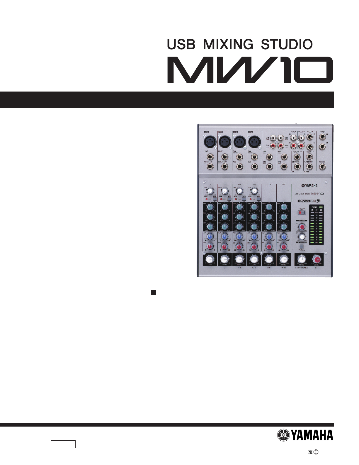
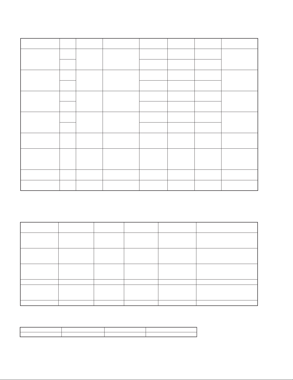
Yamaha MW10 User manual

SERVICE MANUAL
HAMAMATSU, JAPAN
Copyright (c) Yamaha Corporation. All rights reserved. PDF ’06.02
PA 011816
CONTENTS((
((
(目目
目目
目次次
次次
次))
))
)
SPECIFICATIONS(総合仕様).............................................. 3/5
DIMENSIONS(寸法図)........................................................... 7
CIRCUIT BOARD LAYOUT(ユニットレイアウト)................. 7
WIRING(結線図)..................................................................... 8
PANEL LAYOUT(パネルレイアウト)..................................... 9
DISASSEMBLY PROCEDURE(分解手順)........................... 12
LSI PIN DESCRIPTION(LSI 端子機能表)............................. 16
IC BLOCK DIAGRAM (IC ブロック図)................................. 16
CIRCUIT BOARDS(シート基板図)...................................... 17
INSPECTIONS(検査)...................................................... 26/37
BLOCK DIAGRAM & LEVEL DIAGRAM
(ブロック&レベルダイアグラム)
OVERALL CIRCUIT DIAGRAM(総回路図)
PARTS LIST
20060225- オープンプライス

2
MW10
WARNING: CHEMICAL CONTENT NOTICE!
The solder used in the production of this product contains LEAD. In addition, other electrical/electronic and/or plastic (Where
applicable) components may also contain traces of chemicals found by the California Health and Welfare Agency (and possibly
other entities) to cause cancer and/or birth defects or other reproductive harm.
DO NOT PLACE SOLDER, ELECTRICAL/ELECTRONIC OR PLASTIC COMPONENTS IN YOUR MOUTH FOR ANY REASON
WHAT SO EVER!
Avoid prolonged, unprotected contact between solder and your skin! When soldering, do not inhale solder fumes or expose eyes to
solder/flux vapor!
If you come in contact with solder or components located inside the enclosure of this product, wash your hands before handling food.
IMPORTANT NOTICE
This manual has been provided for the use of authorized Yamaha Retailers and their service personnel. It has been assumed that
basic service procedures inherent to the industry, and more specifically Yamaha Products, are already known and understood by the
users, and have therefore not been restated.
WARNING: Failure to follow appropriate service and safety procedures when servicing this product may result in per-
sonal injury, destruction of expensive components and failure of the product to perform as specified. For
these reasons, we advise all Yamaha product owners that all service required should be performed by an
authorized Yamaha Retailer or the appointed service representative.
IMPORTANT: This presentation or sale of this manual to any individual or firm does not constitute authorization certifi-
cation, recognition of any applicable technical capabilities, or establish a principal-agent relationship of
any form.
The data provided is believed to be accurate and applicable to the unit(s) indicated on the cover. The research engineering, and
service departments of Yamaha are continually striving to improve Yamaha products. Modifications are, therefore, inevitable
and changes in specification are subject to change without notice or obligation to retrofit. Should any discrepancy appear to
exist, please contact the distributor's Service Division.
WARNING: Static discharges can destroy expensive components. Discharge any static electricity your body may have
accumulated by grounding yourself to the ground bus in the unit (heavy gauge black wires connect to
this bus.)
IMPORTANT:
Turn the unit OFF during disassembly and parts replacement. Recheck all work before you apply power to
the unit.
Components having special characteristics are marked and must be replaced with parts having specification equal to those
originally installed.
• This applies only to products distributed by Yamaha-Kemble Music (U.K.) Ltd. (2 wires).
WARNING
IMPORTANT NOTICE FOR THE UNITED KINGDOM
Connecting the Plug and Cord
IMPORTANT:
The wires in this mains lead are coloured in accordance with the following code:
BLUE : NEUTRAL
BROWN : LIVE
As the colours of the wires in the mains lead of this apparatus may not correspond with the coloured makings identifying the terminals in
your plug proceed as follows:
The wire which is coloured BLUE must be connected to the terminal which is marked with the letter N or coloured BLACK.
The wire which is coloured BROWN must be connected to the terminal which is marked with the letter L or coloured RED.
Making sure that neither core is connected to the earth terminal of the three pin plug.
印の商品は、安全を維持するために重要な部品です。交換する場合は、安全のために必ず指定の部品をご使用ください。

3
MW10
■ SPECIFICATIONS
Conditions MIN TYP MAX UNIT
To tal Harmonic Distortion (THD+N) 20 Hz - 20 kHz @ +14 dBu 10k ohms, GAIN
(MIC to ST OUT) controls at minimum level, all level controls at nominal level 0.1 %
Frequency Response
(CH INPUT 1-9/10, RETURN, 2TR IN to 20 Hz-20 kHz, nominal output level @ 1 kHz, 10 k ohms, -3 0 1 dB
ST OUT, AUX SEND, C-R OUT, REC GAIN controls at minimum level (CH INPUT 1-5/6), all level
OUT) controls at nominal level
Equivalent Input Noise (CH INPUT 1-2 MIC) -128 dBu
Hum & Noise Residual Output Noise (10 k ohms (ST OUT)) -100 dBu
Rs=150 ohms, Gain=Maximum (CH ST master control at nominal level and all channel LEVEL
INPUT1-2), Hum & Noise are measured controls at minimum level. (ST OUT) -87 dBu
with a -6 dB/octave filter @12.7 kHz; (91 dB S/N)
equivalent to a 20 kHz filter with infinite All channel AUX controls at minimum level. (AUX SEND) -85 dBu
dB/octave attenuation. (89 dB S/N)
ST master control and one channel LEVEL control at -64 dBu
nominal level. (CH INPUT 1, 2) (ST OUT) (68 dB S/N)
CH INPUT 1, 2 MIC to CH INSERT OUT, Rs=150 ohms, 60 dB
GAIN controls at maximum level
CH INPUT 1-5/6 MIC to ST OUT, Rs=150 ohms, 76 dB
GAIN controls at maximum level
CH INPUT 1-5/6 MIC to REC OUT, Rs=150 ohms, 64.2 dB
GAIN controls at maximum level
CH INPUT 1, 2 MIC to AUX SEND, Rs=150 ohms, 70 dB
GAIN controls at maximum level, PRE
Maximum Voltage Gain CH INPUT 1, 2 MIC to AUX SEND, Rs=150 ohms, 76 dB
1 kHz, 10k ohms GAIN controls at maximum level, POST
PAN/BAL: panned hard left or hard right. CH INPUT 3/4-5/6 LINE to ST OUT, Rs=150 ohms, 50 dB
GAIN controls at maximum level
CH INPUT 3/4-5/6 LINE to AUX SEND, Rs=150 ohms, 41 dB
GAIN controls at maximum level, PRE
CH INPUT 3/4-5/6 LINE to AUX SEND, Rs=150 ohms, 47 dB
GAIN controls at maximum level, POST
CH INPUT 7/8-9/10 to ST OUT, Rs=150 ohms, 26 dB
GAIN controls at maximum level
RETURN to ST OUT, Rs=150 ohms 12 dB
2TR IN to ST OUT, Rs=600 ohms 23.8 dB
Crosstalk (1 kHz) Adjacent inputs -70 dB
input to output -70 dB
Where 0 dBu = 0.775 Vrms
Output impedance of signal generator: 150 ohms
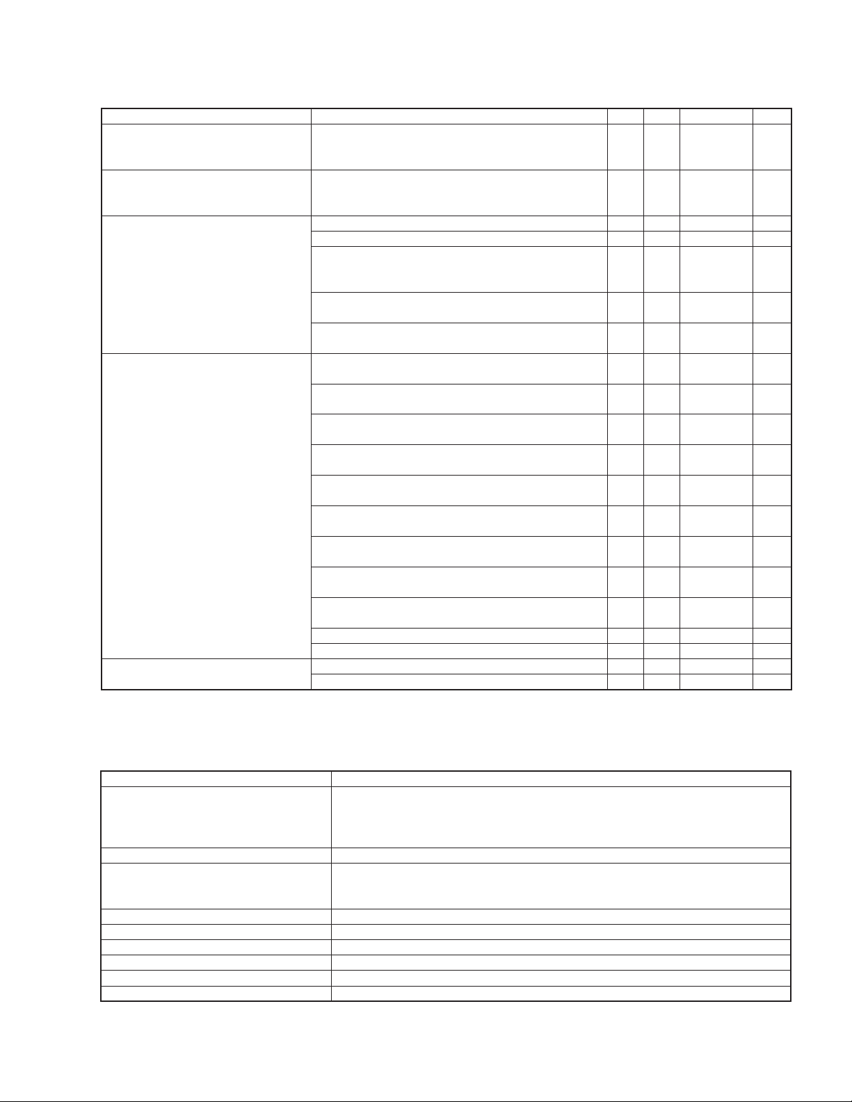
■Electrical Characteristics
Monaural/Stereo CH High Pass Filter 80 Hz 12 dB/octave
Monaural/Stereo CH Equalization ±15 dB (Max. Variation)
HIGH: 10 kHz (shelving)
Turn over/roll-off frequency of shelving, MID: 2.5 kHz (peaking)
3 dB below maximumvariable level LOW: 100 Hz (shelving)
Phantom Power Supplied when Phantom +48 V switch is ON. (XLR-type input jacks)
Monaural/Stereo Input PEAK Indicator On each channel: red indicator lights if post-EQ signal (on stereo channels,
if either post-EQ signal or post-mic-amp signal) comes within 3 dB of the clipping level.
USB Audio Input/Output: 44.1/48 kHz
Included Accessories Power adaptor (PA-10), CD-ROM, USB cable
Power Consumption 19 W
Dimensions (W x H x D) 251 mm x 65 mm x 290.5 mm
Net Weight 1.8 kg
Temperature Range Operating temperature: 0 to 40°C, Storage temperature: -20 to 60°C
■ General Specifications

4
MW10
Input Connector Gain Input Appropriate Sensitivity* Nominal Max. Before Connector
Impedance Impedance Level Clipping Specifications
-60 -72 dBu -60 dBu -40 dBu
MIC INPUT 3 k ohms 50-600 ohms mic (0.195 mV) (0.775 mV) (7.75 mV) XLR-3-31 type
(CH 1, 2) -16 -28 dBu -16 dBu +4 dBu (balanced)
(30.8 mV) (123 mV) (1.23 V)
-34 -46 dBu -34 dBu -14 dBu Phone jack (TRS)
LINE INPUT 10 k ohms 600 ohms line (3.88 mV) (15.5 mV) (155 mV) (balanced [T: hot;
(CH 1, 2) +10 -2 dBu +10 dBu +30 dBu R: cold;
(0.615 V) (2.45 V) (24.5 V) S: ground])
ST CH MIC INPUT -60 -72 dBu -60 dBu -40 dBu
(CH3(L)/CH4(R), 3 k ohms 50-600 ohms mic (0.195 mV) (0.775 mV) (7.75 mV) XLR-3-31 type
CH5(L)/CH6(R)) -16 -28 dBu -16 dBu -10 dBu (balanced)
(30.8 mV) (123 mV) (245 mV)
ST CH LINE INPUT -34 -46 dBu -34 dBu -14 dBu
(CH3(L)/CH4(R), 10 k ohms 600 ohms line (3.88 mV) (15.5 mV) (155 mV) Phone jack
CH5(L)/CH6(R)) +10 -2 dBu +10 dBu +30 dBu (unbalanced)
(0.615 V) (2.45 V) (24.5 V)
ST CH INPUT -22 dBu -10 dBu +10 dBu Phone jack
(CH7(L)/CH8(R), 10 k ohms 600 ohms line (61.5 mV) (245 mV) (2.45 V) (unbalanced);
(CH9(L)/CH10(R)) RCA pin jack
Phone jack (TRS)
CH INSERT IN 10 k ohms 600 ohms line -12 dBu 0 dBu +20 dBu (unbalanced
(CH 1, 2) (195 mV) (0.775 V) (7.75 V) [T: out; R: in;
S: ground])
RETURN (L, R) 10 k ohms 600 ohms line -8 dBu +4 dBu +24 dBu Phone jack
(308 mV) (1.23 V) (12.3 V) (unbalanced)
2TR IN (L, R) 10 k ohms 600 ohms line -22 dBV -10 dBV +10 dBV RCA pin jack
(79.4 mV) (316 mV) (3.16 V)
Where 0 dBu=0.775 Vrms and 0 dBV=1 Vrms
* Input sensitivity: the lowest level that will produce an output of +4 dBu (1.23V) or the nominal output level when the unit is set to maximum gain.
(All level controls are maximum position.)
■ Analog Input Specifications
Output Connectors Output Impedance Appropriate Nominal Level Max. Before Connector Specifications
Impedance Clipping
Phone jack (TRS)
ST OUT (L, R) 150 ohms 10 k ohms line +4 dBu (1.23 V) +20 dBu (7.75 V) (balanced [T: hot; R: cold;
S: ground])
Phone jack (TRS)
AUX SEND (1, 2) 150 ohms 10 k ohms line +4 dBu (1.23 V) +20 dBu (7.75 V) (impedance balanced
[T: hot; R: cold; S: ground])
CH INSERT OUT Phone jack (TRS)
(CH 1, 2) 150 ohms 10 k ohms line 0 dBu (0.775 V) +20 dBu (7.75 V) (unbalanced [T: out; R: in;
S: ground])
REC OUT (L, R) 600 ohms 10 k ohms line -10 dBV (316 mV) +10 dBV (3.16 V) RCA pin jack
Phone jack (TRS)
C-R OUT (L, R) 150 ohms 10 k ohms line +4 dBu (1.23 V) +20 dBu (7.75 V) (impedance balanced
[T: hot; R: cold; S: ground])
PHONES 100 ohms 40 ohms phone 3 mW 75 mW Stereo phone jack
Where 0 dBu=0.775 Vrms and 0 dBV=1 Vrms
■Analog Output Specifications
Connector Format Data Length Connector Specification
USB USB Audio 1.1 16 bit USB B type
■Digital Input/Output Specifications

5
MW10
■ 総合仕様
モノラル、ステレオハイパスフィルター 80Hz12dB/octave
モノラル、ステレオチャンネルイコライザー ±15dB(最大可変幅)
シェルビングタイプのターンオーバー/ロールオフ周波数:最大可
HIGH:10kHz(シェルビングタイプ)
変幅に対して3dB下がったポイント
MID:2.5kHz(ピーキングタイプ)
LOW:100Hz(シェルビングタイプ)
ファンタム電源 PHANTOMスイッチ=オンでDC+48V供給(XLRタイプの入力端子)
モノラル/ステレオインプットPEAKインジケーター
各チャンネル:イコライザー後
(ステレオチャンネルは、イコライザー後またはMICアンプ後)
の信号のレベルが、クリッピングの手前3dBに達すると赤く点灯
USBオーディオ 入出力とも44.1/48kHz
付属品 電源アダプター(PA-10)、CD-ROM、USBケーブル
消費電力 19W
最大外形寸法(W×H×D) 251mmx65mmx290.5mm
質量 1.8kg
温度 動作温度:0〜40℃、保管温度:-20〜60℃
■ 一般仕様
条件 最小 標準 最大 単位
全高調波歪率 (THD+N)20Hz-20kHz@+14dBu10kohms、
(MIC→STOUT) GAINコントロール=最小レベル、 0.1 %
すべてのレベルコントロール=ノミナルレベル
周波数特性
20Hz〜20kHz、ノミナル出力レベル@1kHz、10kohms、
(CHINPUT1〜9/10、RETURN、2TRIN→STOUT、
GAINコントロール=最小レベル(CHINPUT1〜5/6)、
-3.0
0
1.0
dB
AUXSEND、C-ROUT、RECOUT)
すべてのレベルコントロール=ノミナルレベル
入力換算ノイズ(CHINPUT1〜2MIC) -128 dBu
ハム&ノイズ 残留ノイズ(10kohms(STOUT)) -100 dBu
Rs=150ohms、GAINコントロール=最大
STマスターコントロール=ノミナルレベル、 -87 dBu
レベル(CHINPUT1〜2)、@12.7kHz、 全LEVELコントロール=最小レベル(STOUT) (91dBS/N)
-6dB/octaveのローパスフィルター
で測定(@20kHz、-∞dB/octaveフィ
全チャンネルAUXコントロール=最小レベル、(AUXSEND)
-85 dBu
ルターに相当) (89dBS/N)
STマスターコントロール&1LEVELコントロール= -64 dBu
ノミナルレベル(CHINPUT1、2)(STOUT) (68dBS/N)
CHINPUT1、2MIC→CHINSERTOUT、Rs=150ohms、
60 dB
GAINコントロール=最大レベル
CHINPUT1〜5/6MIC→STOUT、Rs=150ohms、 76 dB
GAINコントロール=最大レベル
CHINPUT1〜5/6MIC→RECOUT、Rs=150ohms、 64.2 dB
GAINコントロール=最大レベル
CHINPUT1、2MIC→AUXSEND、Rs=150ohms、 70 dB
GAINコントロール=最大レベル、PRE
最大電圧ゲイン CHINPUT1、2MIC→AUXSEND、Rs=150ohms、 76 dB
1kHz,10kohms GAINコントロール=最大レベル、POST
PAN/BAL:左か右に回し切る CHINPUT3/4〜5/6LINE→STOUT、Rs=150ohms、 50 dB
GAINコントロール=最大レベル
CHINPUT3/4〜5/6LINE→AUXSEND、Rs=150ohms、
41 dB
GAINコントロール=最大レベル、PRE
CHINPUT3/4〜5/6LINE→AUXSEND、Rs=150ohms、
47 dB
GAINコントロール=最大レベル、POST
CHINPUT7/8〜9/10→STOUT、Rs=150ohms、 26 dB
GAINコントロール=最大レベル
RETURN→STOUT、Rs=150ohms 12 dB
2TRIN→STOUT、Rs=600ohms 23.8 dB
クロストーク(1kHz) 入力チャンネル間 -70 dB
入出力チャンネル間 -70 dB
0dBu=0.775Vrms
シグナルジェネレーターの出力インピーダンスは150ohms
■電気的特性

6
MW10
入力端子名称 ゲイン 入力 適合 感度*1 ノミナル 最大
ノンクリップ
端子仕様
インピーダンス
インピーダンス
レベル レベル
-60 -72dBu -60dBu -40dBu
MICINPUT 3kohms 50-600ohms (0.195mV) (0.775mV) (7.75mV) XLR-3-31タイプ
(CH1,2) -16 マイク -28dBu -16dBu +4dBu (バランス型)
(30.8mV) (123mV) (1.23V)
-34 -46dBu -34dBu -14dBu
フォーンジャック(TRS)
LINEINPUT 10kohms 600ohms (3.88mV) (15.5mV) (155mV)
(バランス型[T:ホット、
(CH1,2) +10 ライン -2dBu +10dBu +30dBu R:コールド、
(0.615V) (2.45V) (24.5V) S:グラウンド])
STCHMICINPUT -60 -72dBu -60dBu -40dBu
(CH3(L)/CH4(R), 3kohms 50-600ohms (0.195mV) (0.775mV) (7.75mV) XLR-3-31タイプ
CH5(L)/CH6(R)) -16 マイク -28dBu -16dBu -10dBu (バランス型)
(30.8mV) (123mV) (245mV)
STCHLINEINPUT -34 -46dBu -34dBu -14dBu
(CH3(L)/CH4(R), 10kohms 600ohms (3.88mV) (15.5mV) (155mV) フォーンジャック
CH5(L)/CH6(R)) +10 ライン -2dBu +10dBu +30dBu (アンバランス型)
(0.615V) (2.45V) (24.5V)
STCHINPUT -22dBu -10dBu +10dBu フォーンジャック
(CH7(L)/CH8(R), 10kohms 600ohms (61.5mV) (245mV) (2.45V) (アンバランス型)、
(CH9(L)/CH10(R)) ライン RCAピンジャック
フォーンジャック(TRS)
CHINSERTIN 10kohms 600ohms -12dBu 0dBu +20dBu (アンバランス型
(CH1,2) ライン (195mV) (0.775V) (7.75V) [T:アウト、R:イン
、S:グラウンド])
RETURN(L,R) 10kohms 600ohms -8dBu +4dBu +24dBu フォーンジャック
ライン (308mV) (1.23V) (12.3V) (アンバランス型)
2TRIN(L,R) 10kohms 600ohms -22dBV -10dBV +10dBV RCAピンジャック
ライン (79.4mV) (316mV) (3.16V)
0dBu=0.775Vrms、0dBV=1Vrmsとする
*1入力感度:すべてのレベルコントロールを最大位置としたときに、+4dBu(1.23V)またはノミナル出力が得られる最小入力レベル
■ アナログ入力仕様
出力端子名称 出力 適合 ノミナルレベル 最大ノンクリップ 端子仕様
インピーダンス インピーダンス レベル
フォーンジャック(TRS)
STOUT(L,R) 150ohms 10kohmsライン +4dBu(1.23V) +20dBu(7.75V) (バランス型
[T:ホット、R:コールド、S:グラウンド])
フォーンジャック(TRS)
AUXSEND(1,2) 150ohms 10kohmsライン +4dBu(1.23V) +20dBu(7.75V) (インピーダンスバランス型
[T:ホット、R:コールド、S:グラウンド])
CHINSERTOUT フォーンジャック(TRS)
(CH1,2) 150ohms 10kohmsライン 0dBu(0.775V) +20dBu(7.75V) (アンバランス型
[T:アウト、R:イン、S:グラウンド])
RECOUT(L,R) 600ohms 10kohmsライン -10dBV(316mV)+10dBV(3.16V) RCAピンジャック
フォーンジャック(TRS)
C-ROUT(L,R) 150ohms 10kohmsライン +4dBu(1.23V) +20dBu(7.75V) (インピーダンスバランス型
[T:ホット、R:コールド、S:グラウンド])
PHONES 100ohms 40ohmsフォーン 3mW 75mW ステレオフォーンジャック
0dBu=0.775Vrms、0dBV=1Vrmsとする
■アナログ出力仕様
端子名称 フォーマット データ長 端子仕様
USB USBオーディオ1.1 16bit USBBタイプ
■デジタル入出力仕様

8
MW10
■WIRING(結線図)
(c). Fix the wire by pasting the filament tape to the position of figure.
図の位置にフィラメントテープを貼り、線材を固定します。
* Note that the wire (black) doesn't shut the hole that tightens the
screw.
この時、線材(黒)が、ネジ締め穴を塞がないように注意して下さい。
(c): Filament Tape
(b). Wiring Assy USB10 is fixed with the STYLE PIN that has placed
to the PCB Assy MAIN.
束線USB10をMAINシート上のスタイルピンで固定します。
* Note that the wiring Assy USB10 doesn't approach C501,502,
601,602 of PCB Assy MAIN.
この時、束線USB10がMAINシートのC501,502,601,602に近付
かないように注意して下さい。
(b)C501,502,601,602
(d). Fix the wiring Assy USB10 by pasting the filament tape to the
position of figure.
図の位置にフィラメントテープを貼り、束線USB10を固定します。
* Note that the wiring Assy USB10 doesn't shut the hole of PCB
Assy MAIN.
この時、束線USB10がMAINシートの穴を塞がないように注意
して下さい。
(d): Hole of PCB Assy MAIN.
(a): Wirng Assy AC8
(a): Top Cover
(b): PWB Print (reticulation)
(c): Hole of Screw tightening
1. Processing method of Wiring Assy AC8 (WD350000)
束線AC8(WD350000)の処理
(a). Twist Wiring Assy AC8 three times, and fix to a top cover.
束線AC8を3回捻り、トップカバーに固定します。
(b). Adjust the position so that the wire is arranged within the range
of the PWB print (reticulation).
線材が、基板印刷(網目)の範囲内に配置されるように位置を調
整します。
(a)Hole of PCB Assy MAIN
(b)STYLE PIN
(c)CN101 of the PCB Assy USB
(d): Filament Tape
*1: This connector assembly is not a service parts.
(この束線はサービスパーツ部品ではありません。)
2. Processing method of Wiring Assy USB10 (WG26710)
*1
束線USB10(WG26710)
*1
の処理
(a).
Wiring Assy USB10 is passed through the hole of PCB Assy MAIN.
束線USB10をMAINシートの穴に通します。
(c).
Wiring Assy USB10 is connected with CN101 of the PCB Assy USB.
束線USB10をUSBシートのCN101に接続します。

9
MW10
■ PANEL LAYOUT(パネルレイアウト)
■ Channel Control Section(チャンネルコントロール部)
■ Master Control Section(マスターコントロール部)
q
w
e
r
ty
u
i
q[GAIN] Control
w[PEAK] Indicator
e[ ] Switch (High Pass Filter)
rEqualizer ([HIGH], [MID], and [LOW])
t[AUX] Controls
y[PAN] Control (CHs 1 and 2)
[PAN/BAL] Control (CHs 3/4 and 5/6)
[BAL] Control (CHs 7/8, 9/10)
uChannel [LEVEL] Control
q[GAIN]コントロール
w[PEAK]インジケーター
e[](ハイパスフィルター)スイッチ
rイコライザー([HIGH]、[MID]、[LOW])
t[AUX]コントロール
y[PAN]コントロール(CH1、2)
[PAN/BAL]コントロール(CH3/4、5/6)
[BAL]コントロール(CH7/8、9/10)
u[LEVEL]コントロール
q[PHANTOM +48V] Switch
w[RETURN] Control
e[2TR IN/USB] Control
r[2TR IN/USB] Switch ([TO ST] / [TO C-R])
t[ST Master LEVEL] Control
y[C-R/PHONES LEVEL] Control
uLevel Meter
i[POWER] Indicator
q[PHANTOM+48V]スイッチ
w[RETURN]コントロール
e[2TRIN/USB]コントロール
r[2TRIN/USB]スイッチ([TOST]/[TOC-R])
t[ST]マスターコントロール
y[C-R/PHONES]コントロール
uレベルメーター
i[POWER]インジケーター
Channels
1 and 2
(Monaural)
Channels
3/4 and 5/6
(Stereo)
Channels
7/8
(Stereo)
q
we
r
y
tt
u
t
yy
uu
q
w

10
MW10
q
w
er tyu
io !0
!0
!0
■ Input/Output Section(入出力部)
■ Rear Section(リア部)
qChannel Input Jacks (CHs 1, 2, 3/4, 5/6)
[MIC] jacks
[LINE] jacks
w[INSERT I/O] Jacks (CHs 1 and 2)
eChannel Input Jacks (CHs 7/8, 9/10)
r[2TR IN] Jacks
t[REC OUT] (L, R) Jacks
y[ST OUT] (L, R) Jacks
u[C-R OUT] Jacks
i[SEND] Jacks
[AUX1], [AUX2]
o[RETURN L (MONO)], [R] Jacks
!0 [PHONES] Jack
qチャンネル INPUT 端子(CH1、2、3/4、5/6)
i[MIC]端子
i[LINE]端子
w[INSERTI/O]端子(CH1、2)
eチャンネル INPUT 端子(CH7/8、9/10)
r[2TRIN]端子
t[RECOUT](L、R)端子
y[STOUT](L、R)端子
u[C-ROUT]端子
i[SEND]端子
i[AUX1]、[AUX2]
o[RETURNL(MONO)]、[R]端子
!0 [PHONES]端子
qw e
q[AC ADAPTOR IN] Connector
w[POWER] Switch
e[USB] Connector
q[ACADAPTORIN]端子
w電源スイッチ
e[USB]端子

11
MW10
Connector Polarities
MIC INPUT
Pin 1: Ground
Pin 2: Hot (+)
Pin 3: Cold (-)
LINE INPUT (monaural channels),
ST OUT, C-R OUT
AUX1, AUX2 *
Tip: Hot (+)
Ring: Cold (-)
Sleeve: Ground
Tip: Output
Ring: Input
Sleeve: Ground
PHONES
Tip: L
Ring: R
Sleeve: Ground
RETURN, LINE INPUT (stereo channels) Tip: Hot
Sleeve: Ground
INPUT OUTPUT
Sleeve Tip
Ring
Sleeve Tip
* These jacks will also accept connection to monaural phone plugs. If you use monaural plugs, the connection will be unbalanced.
MIC INPUTINSERTININIININSERT I/O
INSERT I/O
Sleeve Tip
* これらの端子に、モノラルタイプのフォーン端子を使用することもできます。その場合は、アンバランスとなります。
MIC INPUT
ピン1:グラウンド
ピン2:ホット(+)
ピン3:コールド(-)
LINE INPUT(モノラルチャンネル),
ST OUT, C-R OUT
AUX1, AUX2 *
チップ:ホット(+)
リング:コールド(-)
スリーブ:グラウンド
INSERT I/O
チップ:Output
リング:Input
スリーブ:グラウンド
PHONES
チップ:L
リング:R
スリーブ:グラウンド
RETURN,
LINE INPUT(ステレオチャンネル)
チップ:ホット
スリーブ:グラウンド
INPUT OUTPUT
チップ
端子接続の極性
リング
スリーブ
チップ
スリーブ

12
MW10
■DISASSEMBLY PROCEDURE(分解手順)
1. Bottom Case
(Time required: About 1 minute)
1-1 Remove the two (2) screws marked [260]. (Fig.1)
1-2 Remove the five (5) screws marked [265] using a
hexagonal wrench. (Fig.1)
*The spacers [160] have been attached to the five (5)
screws marked [265] respectively. Be careful not to lose
the spacers while disassembling. (Fig.2)
1-3 Under such a condition, lift the top cover up. The bottom
case (with the sheet shield) can then be removed. (Fig.1)
1. ボトムケース
(所要時間:約1分)
1-1 [260]のネジ2本を外します 。(Fig.1)
1-2 [265]のネジ5本を六 角レンチで外します。(Fig.1)
*[265]のネジ5本には、それぞれ[160]のスペーサーが付
いています。作業時にスペーサーを無くさない 様 に 注 意し
て下さい。(Fig.2)
1-3 この状態で、トップカ バ ー部分を上に持ち上げると、ボトム
ケース(シートシールド付 )が外れます。(Fig.1)
(Fig.1) (Fig.2)
[260]: Bind Head Tapping Screw-B 3.0X8 MFZN2W3 (WE774300)
Bタイト+BIND
[265]: Socket Head Cap Screw-P 3X25 MFZN2W3 (WG349100)
Pタイト6角孔付き
Top Cover
(トップカバー)
Bottom Case
(ボトムケース)
[265]
[265]
[265]
[265]
[265]
[260]
[265]
[160]
[160]
[265]
Top Cover
(トップカバー)
MAIN
[160]: Spacer,MIX (WD237400) スペーサーMIX
[265]: Socket Head Cap Screw-P 3X25 MFZN2W3 (WG349100)
Pタイト6角孔付き
2. USB Assembly (USB Circuit Board)
(Time required: About 2 minutes)
2-1 Remove the bottom case. (See procedure 1.)
2-2 Remove the two (2) screws marked [430]. The USB
assembly can then be removed. (Fig.3)
2. USBAssy(USBシート)
(所要時間:約2分)
2-1 ボトムケースを外します。(1項参照)
2-2 [430]のネジ2本を外し、USBAssyを外します。(Fig.3)
[430]
Top Cover
(トップカバー)
(Fig.3)
[430]: Bind Head Tapping Screw-S 3.0X6 MFZN2W3 (WE877900) Sタイト+BIND

13
MW10
3. MAIN Circuit Board
(Time required: About 14 minutes)
3-1 Remove the bottom case. (See procedure 1.)
3-2 Remove USB circuit board. (See procedure 2.)
3-3 Remove the one (1) LEVEL knob (red). (Fig.4)
3-4 Remove the seven (7) LEVEL knob (white). (Fig.4)
3-5 Remove the one (1) screw marked [263], and pull out the
power switch and AC connector from the holes on the rear
of the top cover. (Fig.5)
3-6 Remove the eight (8) screws marked [180A]. (Fig.4)
3-7 Remove the two (2) screws marked [180B]. (Fig.4)
3-8 Remove the twenty-one (21) sets of the hexagon nut and
washer using a box wrench. (Fig.4)
3. MAINシート
(所要時間:約14分)
3-1 ボトムケースを外します。(1項参照)
3-2 USBシートを外します。(2項参照)
3-3 ノブLEVEL(赤)〈ST〉1個を外します。(Fig.4)
3-4 ノブLEVEL(白)〈1、2、3/4、5/6、7/8、9/10、C-R/
PHONES〉7個を外します。(Fig.4)
3-5 [263]のネジ1本を外し、電源スイッチとA Cコネクターをトッ
プカバー のリア側の穴から外します。(Fig.5)
3-6 [180A]のネジ8本を外します。(Fig.4)
3-7 [180B]のネジ2本を外します。(Fig.4)
3-8 六角ナットとワッシャ2 1セットをボックスレンチ で 外します 。
(Fig.4)
Hexagonal nut & Washer
(六角ナット、ワッシャー)
Claw
(ツメ)
AC connector
(ACコネクター)
Power switch
(電源スイッチ)
Top Cover
(トップカバー)
[263]
Support AC
(サポートAC)
(Fig.4)
(Fig.5)
[180]: Bonding Tapping Screw-B 3.0X10 MFZN2W3 (WG349000) Bタイト+BOND
[263]: Bind Head Tapping Screw-S 3.0X6 MFZN2W3 (WE877900) Sタイト+BIND
Top Cover
(トップカバー)
Guard, PFL
(ガードPFL)
[180A] [180B]
Hexagon nut & washer
(六角ナット、ワッシャー)
LEVEL knobs (WHITE)
(ノブLEVEL(白))
LEVEL knob (RED)
(ノブLEVEL(赤))

14
MW10
3-9 Lift up the top cover to remove the MAIN circuit board
(with knobs, button and Meter cover). (Fig.2)
*The spacers [160] have been attached to the five (5) screws
marked [265] respectively. Be careful not to lose the spacers
while disassembling. (Fig.2)
*The guard PFL has been attached to the place of PHANTOM
+48V on the top cover. Be careful not to lose the guard while
disassembling. (Fig.4)
*When installing the MAIN circuit board and the top cover,
confirm whether the heads of LEDs and spacers correctly come
out of the corresponding holes on the top cover. (Fig.6)
*The knobs, buttons and supporting fixtures on the MAIN circuit
board are not components of the circuit board.
When replacing the MAIN circuit board, be sure to remove these
parts and install it the new MAIN circuit board according to
the following procedure.
3-10 Pull out the thirty-six (36) VR knobs from the MAIN circuit
board. (Fig.7)
*When installing the VR knobs, be careful of the color of the
knob. (Fig.7)
3-11 Remove the PFL button and the five (5) HPF buttons from the
MAIN circuit board. (Fig.7)
3-12 Detach the meter cover from the meter reflector. (Fig.7)
3-9 トップカバ ーを上 に持ち上 げ、MAINシート(ノブ、ボタン、ウイ
ンドウ METER付)を外します。(Fig.2)
*[265]のネジ5本には、それぞれ[160]のスペーサーが付い
ています。作業時にスペーサーを無くさない様に注 意して下
さい 。(Fig.2)
*トップカバーの[PHANTOM+48V]の位置にはガードPFL
が取り付けられています 。 作業時にガードを無くさない様に注
意して下さい 。(Fig.4)
*MAINシートとトップカバーの再組立時に、LEDの頭とスペー
サーがパネルの穴から正しく出ているか 注 意して 下さい 。
(Fig.6)
*MAINシート上のノブ、ボタン、ウィンドウMETERは、シートの
構成部品ではありません。MAINシートを交換する際は、以下
の手順でこれらの部品を取り外して新しい MAINシートに取
付けて下さい。
3-10 MAINシートからノブVRを36個抜き取ります 。(Fig.7)
*再取付け時は、ノブVRの色に注意して下さい。(Fig.7)
3-11 MAINシートから、ボタンPFLを1個、ボタンHPFを5個、抜き取り
ます 。(Fig.7)
3-12 リフレクター METERからウィンドウMETERをはがします。
(Fig.7)
(Fig.6)
(LED) (Spacer)
OK NGOK NG Top Cover
(トップカバー)
Side View
(側面図)
MAIN
(Fig.7)
Meter cover
(ウインドウMETER)
PFL button
(ボタンPFL)
HPF button
(ボタンHPF)
HPF buttons
(ボタンHPF)
VR knobs (WHITE)
(ノブVR(白))
VR knobs (GREEN)
(ノブVR(緑))
VR knobs (BLUE)
(ノブVR(青))
VR knobs (RED)
(ノブVR(赤))
MAIN
VR knobs (RED)
(ノブVR(赤))
VR knobs (WHITE)
(ノブVR(白))

15
MW10
4. Power Switch and AC Connector
(Time required: About 4 minutes)
4-1 Remove the bottom case. (See procedure 1.)
4-2 Remove the one (1) screw marked [263], and pull out the
power switch and AC connector from the holes on the rear
of the top cover. (Fig.5)
4-3 Remove the power switch by pressing its claw. (Fig.5)
4-4 To remove the AC connector, remove the hexagon nut and
flat washer. (Fig.5)
*Unless the wirings connected to the AC connector are
removed, the AC connector cannot be removed from the
support AC.
5. Fuse (Time required: About 11 minutes)
5-1 Remove the MAIN circuit board. (See procedure 3 (3-1 to
3-9).)
5-2 Exchange the fuse (F01/F02) for new one on the MAIN
circuit board. (Fig.8)
4. 電源スイッチとACコネクター
(所要時間:約4分)
4-1 ボトムケースを外します。(1項参照)
4-2 [263]のネジ1本を外し、電源スイッチとA Cコネクターをトッ
プカバ ー のリア側の穴から外します。(Fig.5)
4-3 電源スイッチ のツメを 押して 、電源スイッチを外します 。
(Fig.5)
4-4 六角ナットと平ワッシャを外して ACコネクターを外します 。
(Fig.5)
*ACコネクターは、接続されている線材を外さないとサポー
トACとは分離できません。
5. ヒューズ交換(所要時間:11分)
5-1 MAINシートを外します。(3項の3-1〜3-9参照)
5-2 MAINシート上 のヒュー ズ(F01、F02)を交換します。
(Fig.8)
Fuse F01
Fuse F02
MAIN
(Fig.8)

16
MW10
■ LSI PIN DESCRIPTION(LSI 端子機能表)
PIN
NO. I/O FUNCTIONNAME I/O FUNCTIONNAME
1
2
3
4
5
6
7
8
9
10
11
12
13
14
D+
D-
V
BUS
DGNDU
HID0
HID1
HID2
SEL0
SEL1
V
CCCI
AGNDC
V
IN
L
V
IN
R
V
COM
I/O
I/O
-
-
I
I
I
I
I
-
-
I
I
-
USB differential input/output plus
USB differential input/output minus
Connect to USB power (V
BUS
)
Digital ground for USB transceiver
HID key state input(mute), active high
HID key state input(volume up),active high
HID key state input(volume down),active high
Must be set to high
Must be set to high
Internal analog power supply for codec
Analog ground for codec
ADC analog input for L-channel
ADC analog input for R-channel
Common for ADC/DAC(VCCCI/2)
15
16
17
18
19
20
21
22
23
24
25
26
27
28
V
OUT
R
V
OUT
L
V
CCP1I
AGNDP
V
CCP2I
XTO
XTI
AGNDX
V
CCXI
TEST0
TEST1
DGND
V
DDI
SSPND
O
O
-
-
-
O
I
-
-
I
O
-
-
O
DAC analog output for R-channel
DAC analog output for L-channel
Internal analog power supply for PLL
Analog ground for PLL
Internal analog power supply for PLL
Crystal oscillator output
Crystal oscillator input
Analog ground for oscillator
Internal analog power supply for oscillator
Test pin, must be connected to GND
Test pin, must be left open
Digital gronud
Internal digital power supply
Suspend flag, active low
(Low: suspend, High: operational)
PCM2900E/2K (X7143A00) USB PROTOCOL CONROLLER
USB: IC101
PIN
NO.
LB1412M(X5838A00)
LED Driver
MAIN: IC803, 805
13
10
9
8
16
7
6
5
4
3
2
23
22
21
20
19
18
17
14 1512
11
+
-
+
-
+
-
+
-
+
-
+
-
+
-
+
-
+
-
+
-
+
-
+
-
+
-
+
-
OSC
CURENT
DRIVER
CURENT
DRIVER
VZ
OUT2
RESET OSC ILED
D1
D2
D3
D4
D5
D6
D7
D8
D9
D10
D11
D12
IN2
OUT1
IN1
VCC
GND
R
SQ
R
SQ
Q
R
SQ
Q
R
SQ
Q
R
SQ
Q
■IC BLOCK DIAGRAM(IC ブロック図)
NJM4556AL (XP844A00)
Dual Operational Amplifier
OUT
A
-
A
+
A
-
V
+
V
OUT
B
-
B
+
B
AB
12345
678
MAIN: IC806
NJM4580E-D (XT157A00)
NJM4558M (X5676A00)
NJM2068M-D (X3505A0)
Dual Operational Amplifier
MAIN:IC101, 201, 301, 401, 801, 804
MAIN:IC103, 304, 404, 503, 603(1st lot)
MAIN:IC302, 402, 501, 601, 802
USB:IC103, 104
●
1
2
3
4-V
8
7
6
5
Output A +V
Non-Inverting
Input A
-DC Voltage Supply
+DC Voltage
Supply
Output B
Inverting
Input B
Non-Inverting
Input B
Inverting
Input A
+-
+-
BA4560RF-E2 (X6897A00)
Dual Operational Amplifier
MAIN:IC202, 303, 403, 502,
IC602, 701, 702, 807
IC103,304,404,503,603(2nd lot~)
●
1
2
3
4-V
8
7
6
5
Output A +V
Non-Inverting
Input A
-DC Voltage Supply
+DC Voltage
Supply
Output B
Inverting
Input B
Non-Inverting
Input B
Inverting
Input A
+-
+-

17
MW10
to MAIN-CN801
CONTENTS
USB Circuit Board (X7196C0)......................................................................................... 17
MAIN Circuit Board (X6347D0) .................................................................................. 18-21
MAIN Circuit Board (X6347E0) .................................................................................. 22-25
■CIRCUIT BOARDS(シート基板図)
Component Side(部品側)
Pattern Side(パターン側)
●USB Circuit Board
2NA-WG33610 Note: See parts list for details of circuit board component parts.
注:シートの部品詳細はパーツリストをご参照ください。
*As for version B, a part of silk print is different.
(B バージョンは表面印刷が一部異なります。)

18
MW10
C143,
C401-C402
C301-C302
C201-C202
C101-C102
Apply sillicon grease to the shaded area.
斜線部にシリコングリスを塗る事。
C101,C102,C201,C202,C301,C302,C143,C401,C402
should fix adjacent CAP ELECTRITIC with adhesives.
The Electritic in he PWB silk shaded area is a thing
fixed to he PWB with adhesives.
C101,C102,C201,C202,C301,C302,C143,C401,C402は
隣り合うケミコン同士を接着剤で固定すること。
基板シルク斜線部のケミコン(4カ所)は基板に
接着剤で固定すること。
ADHESIVE
CAP ELECTRITIC
INSERT
I/O
INSERT
I/O
LINE
LINE
MIC
MIC
MIC
MIC
4R
6R
3L
(MONO)
5L
(MONO)
8R
7L
7L 8R
9L 10R 9L 10R
7L
INSERT
I/O
INSERT
I/O
LINE
LINE
MIC
MIC
MIC
MIC
4R
6R
3L
(MONO)
5L
(MONO)
8R
7L
7L 8R
9L 10R 9L 10R
7L
INSERT
I/O
INSERT
I/O
LINE
LINE
MIC
MIC
MIC
MIC
4R
6R
3L
(MONO)
5L
(MONO)
8R
RETURN
R
7L
RETURN
L(MONO)
SEND
AUX
2
AUX
1
C-R OUT
R
C-R OUT
L
PHONES
ST OUT
R
ST OUT
L
REC
OUT
LR
LR
2TR
IN
7L 8R
9L 10R 9L 10R
RETURN
R
7L
RETURN
L(MONO)
SEND
AUX
2
AUX
1
C-R OUT
R
C-R OUT
L
PHONES
ST OUT
R
ST OUT
L
REC
OUT
LR
LR
2TR
IN
RETURN
R
RETURN
L(MONO)
SEND
AUX
2
AUX
1
C-R OUT
R
C-R OUT
L
PHONES
ST OUT
R
ST OUT
L
REC
OUT
LR
LR
2TR
IN
RETURN
R
RETURN
L(MONO)
AUX
2
AUX
1
C-R OUT
R
C-R OUT
L
PHONES
ST OUT
R
ST OUT
L
REC
OUT
LR
LR
RETURN
R
RETURN
L(MONO)
SEND
AUX
2
AUX
1
C-R OUT
R
C-R OUT
L
PHONES
ST OUT
R
ST OUT
L
REC
OUT
LR
LR
2TR
IN
A
A'
●MAIN Circuit Board (X6347D0)
Note: See parts list for details of circuit board component parts.
注:シートの部品詳細はパーツリストをご参照ください。

19
MW10
Note: See parts list for details of circuit board component parts.
注:シートの部品詳細はパーツリストをご参照ください。
Component Side(部品側)
HIGH MID LOW AUX PAN LEVEL
PEAK
PEAK
PEAK
PEAK
PAN/BAL
PAN/BAL
BAL
BAL
2TR IN/USBRETURN
TO ST
TO C-R
PHANTOM
+48V
PEAK
PEAK
PEAK
PEAK
PAN/BAL
PAN/BAL
BAL
BAL
2TR IN/USBRETURN
TO ST
TO C-R
PHANTOM
+48V
E
RT
O
E
RT
O
R
6R
8R
0
R
E
RT
O
E
RT
O
R
6R
8R
0
R
E
RT
O
E
RT
O
R
6R
8R
U
RN
R
U
X
2
O
NES R
L
ST
0
R
U
RN
R
U
X
2
O
NES R
L
ST
U
RN
R
U
X
2
O
NES R
L
ST
1
2
3/4
5/6
7/8
9/10
C-R /
PHONES
ST
SCALE : 90/100
to USB-CN101
U
RN
R
U
X
2
O
NES
U
RN
R
U
X
2
O
NES R
L
ST
PEAK +3 0 -3 -7 -15
+5 +1 -1 -5 -10 -20
GAIN
A
A'
2NA-WG23970 1
Other manuals for MW10
5
Table of contents
Other Yamaha Recording Equipment manuals

Yamaha
Yamaha TG100 Parts list manual

Yamaha
Yamaha TG-33 User manual

Yamaha
Yamaha DSP-100 User manual

Yamaha
Yamaha YDG2030 User manual

Yamaha
Yamaha ACU16-C User manual

Yamaha
Yamaha MY8-SDI-ED User manual

Yamaha
Yamaha SFGII User manual

Yamaha
Yamaha REV-5 User manual

Yamaha
Yamaha MOTIF-RACK ES Instruction Manual

Yamaha
Yamaha TX-216 User manual

Yamaha
Yamaha Steinberg MR816SCX User manual

Yamaha
Yamaha PM1800 User manual

Yamaha
Yamaha CDR-HD1000 User manual

Yamaha
Yamaha CDR200t User manual

Yamaha
Yamaha TX-802 User manual

Yamaha
Yamaha TG300 User manual

Yamaha
Yamaha O2R User manual

Yamaha
Yamaha SPX990 User manual

Yamaha
Yamaha TG77 User manual

Yamaha
Yamaha MU100R User manual