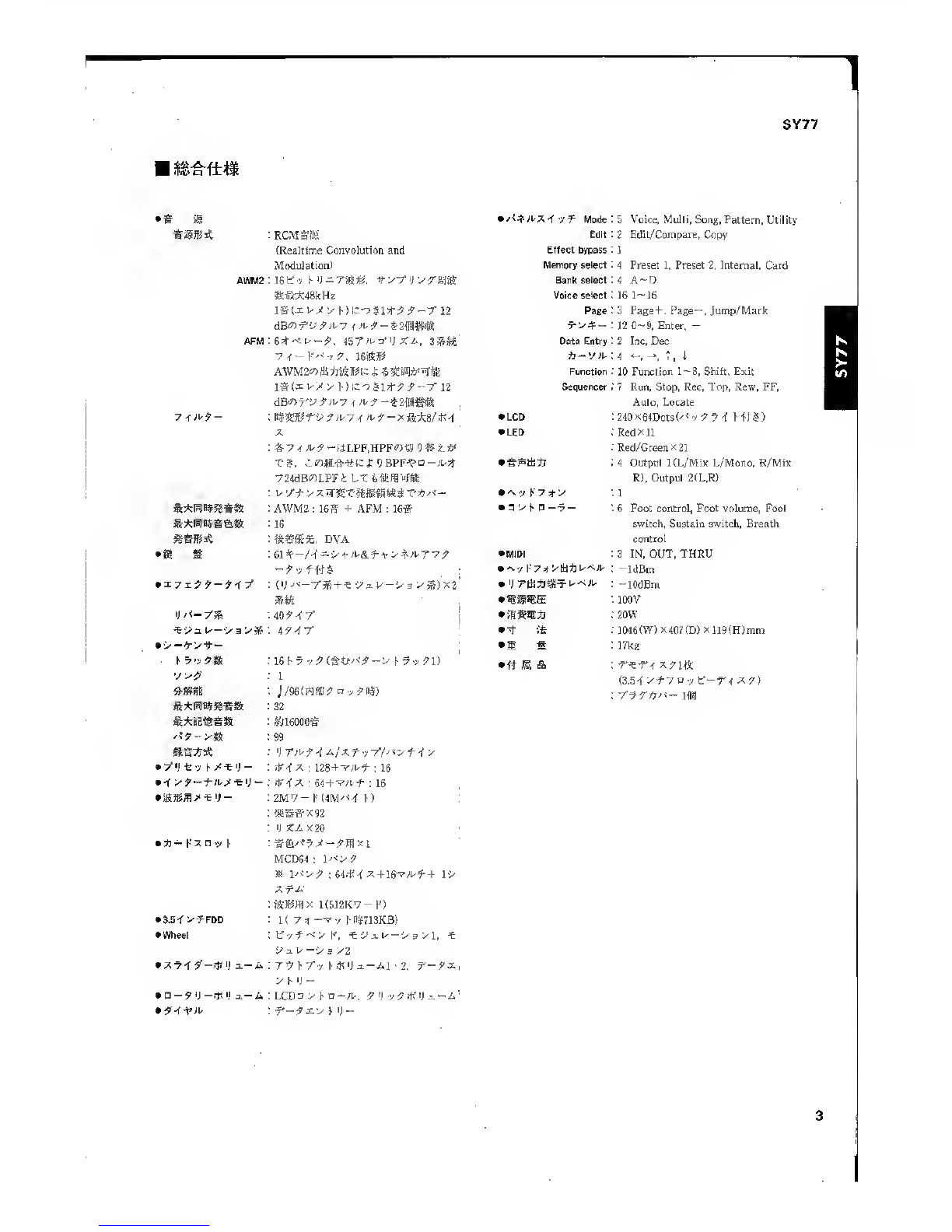
Yamaha SY-77 User manual

•CONTENTS (S>^)
SPECIFICATIONS 2
PANEL LAYOUT !•) 4
CIRCUIT BOARD LAYOUT (^--y I- h) 6
BLOCK DIAGRAM {-^ u-j 97^7L.) 8
DISASSEMBLY PROCEDURE 10
ASSEMBLY PRECAUTIONS 15
LSI PIN DESCRIPTION 17
1C BLOCK DIAGRAM Ocya-y^m) 23
CIRCUIT BOARDS (->-t-»^5EI) 25
ERROR MESSAGES (x-7-> -y-b-v) 44
TEST PROGRAM (t^:^ I- ^^7 A) 48/72
MIDI DATA FORMAT (MIDI t'- 5?7 ;r-V'y h) 94
MIDI IMPLEMENTATION CHART 111
PARTS LIST
YAMAHA CORP.
HAMAMATSU. JAPAN
2.27K-885 ©Printed in Japan '90.01
SY77

SY77
SY77
IMPORTANT NOTICE
This manual has been provided for the use of authorized Yamaha Retailers and their service personnel. It
has been assumed that basic service procedures inherent to the industry, and more specifically Yamaha
Products, are already known and understood by the users, and have therefore not been restated.
WARNING: Failure to follow appropriate service and safety procedures when servicing this product
may result in personal injury, destruction of expensive components and failure of the
product to perform as specified. For these reasons, we advise all Yamaha product owners
that all service required should be performed by an authorized Yamaha Retailer or the
appointed service representative.
IMPORTANT: The presentation or sale of this manual to any individual or firm does not constitute
authorization, certification, recognition of any applicable technical capabilities, or
establish a principle-agent relationship of any form.
The dau provided is believed to be accurate and applicable to the unit(s) indicated on the cover. The
research, enpneering, and service departments of Yamaha are continually striving to improve Yamaha
products. Modifications are, therefore, inevitable and changes in specification are subject to change without
notice or obligation to retrofit. Should any discrepancy appear to exist, please contact the distributor’s
Service Division,
WARNING: Static discharges can destroy expensive components. Discharge any static electricity your
body may have accumulated by grounding yourself to the ground buss in the unit (heavy
gauge black wires connect to this buss).
IMPORTANT: Turn the unit OFF during disassembly and parts replacement. Recheck aM work before
you apply power to the unit.
This product uses alithium battery for memory back-up.
WARNING: Lithium batteries are dangerous because they can be exploded by improper handling.
Observe the following precautions when handling or replacing lithium batteries.
•Leave lithium battery replacement to qualified service personnel.
•Always replace with batteries of the same type.
•When installing on the PC board, solder using the connection terminals provided on the battery cells.
Never solder directly to the cells. Perform the soldering as quickly as possible.
•Never reverse the battery polarities when installing.
•Do not short the batteries,
•Do not attempt to recharge these batteries.
•Do not disassemble the batteries.
•Never heat batteries or throw them into fire.
ADVARSEL!
Lithiumbatteri. Eksplosionsfare.
Udskiftning ml kun foretages af en sagkyndig, og som beskrevet iservicemanualer.
1

SPECIFICATIONS
*Tone generator:
•Keyboard:
•DSP effects:
•Sequencer:
•Memory:
•Controllers:
•Display:
•Terminals:
•Power requirements:
ePower consumption;
•Dimensions;
•Weight:
•Output level:
•Accessory:
Realtime Convolution and Modulation (RCMl
AWM2; 16bitlinear waveform data, maximum 43l< Hz
sampling frequency
AFM: 6operators, 45 algorithms, 3feedback loops,
16 waveforms, modulation from AWM output
Filter; Time variant MR (infinite Impulse response!
digital filters, 2filters for esch element (maximum of
8fillers per voice)
Maximum simultaneous notes: 16notes AWM -f 1
6
notes AFM
Maximum simultaneous timbres; 16
Note assignment; Last note priority, DVA (dynamic
voice aiiocation)
61 notes, ksy velocity sarrsitivity, channel aftertouch
(reverb effeci+moduiation effect) >2
Reverb effects: 40 types
Modulation effects: 4types
Tracks: 16(15tracks+l pattern track)
Songs: 1
Resolution: 1/96 of aquarter note (for internal clock)
Maximum simultaneous notes: 32
Capacity: approximately 16,000 notes
Panetns: 99
Recording: realtIme/step/punch In
Preset memory: 128 voices, 16multl$
Internal memory: 64 voices, 16 mulds
Waveform memory: 2Mwords (4 Mbytes), 112
sounds
Card slots; synthesizer data *1,waveform data x1
Disk: 3.5" floppy disk drive
(713K byte formatted I
Wheels; PITCH, MODULATION 1, MODULATION 2
Slider: OUTPUT 1, OUTPUT 2, DATA ENTRY
Knobs: LCD contrast, click volume
Dial: data entry dial
Panel switches: MODE x5, EDIT/COMPARE, COPY/
SAVE, EF.BYPASS, SEQUENCER x7, SHIFT, function
x8, EXIT, PAGE <>, JUMP/MARK, cursor AV
<3 >, -1/NO, +1/YES, numeric keypad 0-9,
MEMORYX4, BANKx4, voice selectxl6
LCD: 240 X64 pixels (backlltl
LED; red X11, red/green x21
Audio output; OUTPUT 1(L/MIX, L/MONO, R/MIX R),
OUTPUT 2(L, R), PHONES Controller: BREATH, FOOT
V(XUME, FOOT CONTROLLER, SUSTAIN, FOOT
SWITCH
MIDI; IN, OUT, THRU
U.S. &Canadian models: 120V
European &Australian models; 220-240V
U.S. &Canadian models: 28W
European &Australian modela: 28W
1046 (W)x407 (D)x119 (HI mm
17kg
Headphones: -IdBm
Output terminals: -lOdBm
Flopply disk (3.6 inch) xi
Plug cover x1

SY77
AWM2 :
AFM
7-f Jl-?-
S«»it
•a s
•I7i77-^"f 7"
i;a-7s
^-7i U-— •> a:
•->—>>••)•-
•J>9
'<9-y&
assst
•T’y-fe'y I- ij -
»< :
•33- K7D 2< h
•3.5-f y^FDD
•Wheal
•77-f5'-^i;i-A :
•-?g-3<ij i-i, :
•j'-f+A.
:RCMg’iSi
(Realtime Convolution and
Modulation)
:lecv 1-
»ft:*:48kH2
h)IC'3Slt73'-7' 12
dBWf'i’ ?/i-7 ^;u 3- -S2fliffiiR
457>y^')Xi.^ 3mUi
7^-K'<-/7. ISiftW
AWM2co,^:ijS)f#lc J:
h)(C'03l^7:?-r 12
dBi?)7'i3?7U7^3U?-$ 2(H4Se
:<
X
:*7^;u ?-IS LPF.HPFW«01!5
1
•C8, ^cott-S-StcJ: 0BPF-?D-/u;r
724dB<^LPF tLX 6ffill =filg
uy+vxsrsxsffiwsixt^/t-
AWM2 :16ff +AFM :16Sf
16
«t«a. DVA
f-«3
3^Kc
:40:?'f7‘
:4y-4r
16 h7y7(t-tfy’7 -> h7771)
1
J/96(FJffi7D /7lt)
32
I'neooo*
99
')7iy9A^!XT-j-7l'^>7‘{>
iK-t X:128 +-5’;i'f :16
4<-<X :64 +-7>t-f- :16
2M7- K(4My'--^ 1)
*SffEfx92
UX2.X20
:taytxy-ysxi
MCD64 :l''-3'7
»ly‘77 :64-'K'( X+lS7’;i-t+ l‘>
XrA K512K7- K)
1( 7t—77 Hi#713KB)
e-yf-'X yK, ti>i k-->3 €
‘y —y 3yz
:77 ^7 yI- d<il 0.-2.1 -2, ?'-7i,
>(-')-
:LCDs >)• n-/u. 7') /7iK>) '
:r-9x.y hij-
•/<:f;ux-1' 77" Mode
Edit
Effect bypass
Memory select
Bank select
Voice select
Page
T-y^~
Data Entry
33 —yjp
Function
Sequencer
•LCD
LED
•e^m*
•Y7^y
•ay kQ--7 —
•MIDI
•'^yY7tyHity'<ii-
•t-;£
•Is
•# E &
:5Voice, Multi, Song, Pattern, Utility
:2Edit/Compare, Copy
.1
:4Preset 1, Preset 2, Internal. Card
:4A~D
:16 1~16
;3 Page +,Page-, Jump/Mark
:12 0~9, Enter, -
;2 Inc, Dec
:4 I
:10 Function 1-8, Shift, Exit
;7Run, Stop, Rec, Top, Rew, FF,
Auto, Locate
;240X64Dots(yf v75-( H43)
:Red XU
:Red/Green x21
;4Output ICL/Mix L/Mono, R/Mix
R), Output 2(L,R)
:1
i6Foot control, Foot volume, Foot
switch, Sustain switch. Breath
control
3 IN, OUT. THRU
-IdBm
-lOdBm
lOOV
20W
1046 (W) X407(D) xll9CH)mm
17kg
-7'"Ef’^ X71«C
(3.5-f >-? 70-y b'-f'y X7)
:ms
3
SY77

0
oSQ iSJCSCiD
mm

SY77

SY77

SY77
DISASSEMBLY PROCEDURE
1.
Bottom Cover Assembly (refer to fig. 1.)
1-1. Remove the nineteen (19) screws ®(4.Ox
10 bonding head tapping screw), the Bottom
cover assembly can be removed.
This will give you access to the DMI, DM2,
PS circuit boards. Floppy disk drive unit and
Wheel assembly.
2. DMI Circuit Board (refer to fig.2|
2-1. Remove the Bottom cover assembly, (see
procedure 1.)
2-
2. Remove the six (6) screws ®(4.0 x10 bind
head tapping screw], the DMI circuit board
can be raised.
After the connectors have been disconnected,
the DMI circuit board can be taken out of
the unit completely.
3. DM2 Circuit Board (refer to flg.2|
3-
1. Remove the Bottom cover assembly, (see
procedure 1.)
3-
2. Remove the six (6) screws ©(4.0 x10 bind
head tapping screw), the DM2 circuit board
can be raised.
After the connectors have been disconnected,
the DM2 circuit board can be taken out of
the unit completely.
4. PS Circuit Board (refer to fig. 2.)
4-
1. Remove the Bottom cover assembly, (see
procedure 1.)
4-2. Remove the screw ®(4.Ox 10 bonding head
tapping screw) to remove the AC panel.
4-3. The PS circuit board can be removed by re-
moving the four (4) screws ©(4.0 x10 bind
head tapping screw) and disconnecting the
connectors.
1. mmAss-y <7)9^ i:fj (mi#®)
1-1. vJ19-2t^(4 h4-x)
2, DM 1•>- (H 2#B5)
2-1. H^gAss'yS-^Li-f. (UK#.#.)
2-
2. 6:^(4 xIO-'nM >t
3, DM2 (EI2#B§)
3-
1. JStSAss'ytJT-Lif,
3-
2. 6#(4 xIO'n'T t,
4, PSix- h<7)^(,:*t (112#BB)
4-
1. lifijAss'yS-Jd-LJ-t-. (IIR#,#)
4-2. 1#(4 xio^ior-f yi7Bf''f h4-y)
4-3. y42fs(4 >K? Vb.
10
SY77

SY77
SY77
I
5. Power Transformer (refer to fig. 2.)
5-1. Remove the Bottom cover assembly, (see
procedure 1.)
5-2. Remove the PS circuit board, (see procedure 4.1
5-
3. Remove the two (2) screws ©(4.0 >: 10 bind
head tapping screw) to remove the Power
transformer.
6. Floppy Disk Drive Unit (refer to fig. 2and fig. 3)
6-
1. Remove the Bottom cover assembly, (see
procedure 1.)
6-2. Remove the three (3) screws ©(4.0 x10 bind
head tapping screw) and disconnect the con-
nectors, the Floppy disk drive unit can be taken
out of the SY77 unit.
6-3. To remove the FDD holder from the Floppy
disk drive unit, remove the four (4) screws ®
(3.0x6 bind head tapping screw).
5. (ia2#SiO
5-1. (£1SAss'yS-HL*1-o
5-2.
5-
3. 2^(4 xlO/<^- >Kj? yy) i
6. FDDCOfl-b:^ (132, 3#M)
6-
1. SISAss'y^J^Lito
6-2.yt
FDD Ass’y^SstO^hLJI-o FDD
X6'<-f >
LTKOJtLSI-,
7. CARD Circuit Board (refer to fig. 4)
7-1. Remove the Bottom cover assembly, (see
procedure 1.)
7-2. Remove the DM1 circuit board, (see procedure
2.)
7-
3. After the three (3) screws ®(4.0 x10 bind
head tapping screw) have been removed, the
CARD circuit board can be removed.
8. JKAN Circuit Board (refer to fig. 4and fig. 5)
8-
1. Remove the Bottom cover assembly, (see
procedure 1.1
8-2. Remove the DIV11 and DM2 circuit boards.
(see procedures 2and 3.)
8-3. Remove the ten (10) screws ®(4.0 x10bond-
ing head tapping screw) on the rear panel and
three (3) screws ®(4,0x 10 bind head tapping
screw), the JKAN circuit board can be removed.
7. CARD->- K7)^f^ (S4#ff§)
7-1. mSAss'yS-tfLJto
7-2. DM1
b
(2iS#M)
7-
3. ®OT->’3^{4 X10.'-‘M >K:? •/ t.
8. JKAN->- (04. 5#SS)
8-
1. IgtSAss’y^-HLSt. (l<M#ffi)
8-2. DM1 •>- I- tDM2 X- b5-51-Lato
8-3. 35b:(4 xlO^M >V^-y v) i,
ij j: 0±rtt'i'4®7)4-yi0’ls(4 xio
11

SY77
9. Keyboard Assembly (refer to fig. 6.)
9-1- Remove the Bottom cover assembly, (see
procedure 1.)
9-2. Remove the DM! and DM2 circuit boards,
(see procedures 2and 3.)
9-3. Remove the PS circuit board, (see procedure 4.)
9-4. The Keyboard assembly can be removed by
removing the five (5) screws (4.0 x10 bind
head tapping screw) and four (41 screws ®
(4.0 X16 bind head tapping screw).
9- SMAss’ycO^L::? (0 6#.^)
9-1. fi^StAss’y^nLi-r.
9-2. DM1 V- ftDM2 h
9-3.
9-4. 5i=(4 xlO^'M >'X •>') t
4^U yVf -/ S:
Tt-L-rmO^LSi-o
dig. 6)
10. PNAB and PNC Circuit Boards (refer to fig. 4
and fig. 7)
10-1. Pull out the konbs on the Control panel.
10-2. Remove the Bottom cover assembly, (see
procedure 1.)
10-3. Remove the DM1 and DM2 circuit boards,
(see procedures 2and 3.)
10-4. Remove the PS circuit board, (see procedure
4.)
10-5. Remove the JKAN circuit board, (see proce-
dure 8.)
10-6. Remove the Keyboard assembly, (see proce-
dure 9.)
10-7. Remove the fourteen (14) screws ®> (4.0x
10 bind head tapping screw) to remove the
Center angle bracket.
10. PNAB->- I- tPNC->- |-d>9f L'^ (04.7#fiH)
10-1. 9, X9T Kd^'J =
10-2. (e1SAss’y5-?l-Lt1-,
10-3. DM1
h
kDM2
(2 13il#.aa>
10-4. psi'- )• ^51-Lgt.
10-5. JKAN->- 1- ?-ld-Lito (8i«#.fS)
10-6- aSSAss’yi-^t^ t. (9»0#M)
10-7. ®c^d--xl4>k(4 xio^n'T VK:? •/ y)
i^LT, 4iyf’-ry-7’>l'i:M')9VLt-r,
12
SY77

SY77
SY77
10-8. PNAB circuit board removal
10-8-1 .Remove the CARD circuit board, (see proce-
dure 6.)
10-8-2. Remove the three (3) screws ®(4.0 x10
bind head tapping screw) to remove the
Card guide.
10-8-3. After the seven (7) screws ©(4.0x10
bind head tapping screw) have been re-
moved, the PNAB circuit board can be re-
moved.
*The PNAB circuit board is connected to
the PNC circuit board with wire harnesses.
10-9. PNC circuit board removal
10-9-1. After the eight (8) screws (Q) (4.0x10
bind head tapping screw) have been re-
moved, the PNC circuit board can be re-
moved.
10-8. PNABi-- i-con-LIj
10-8-1. CARD->-hS'nL*1-, (635#.®.)
10-8-2. xlO-'-r-f >y-y ^i>)
KS'KOM-Lil-.,
10-8-3. xlO'-r-f >V9-v
g'JI-i+tiPNAB-,'-
PNC-^-h iJI-L
10-9. PNC->- V<n9\-Li}
10-9-1. @t04->^8 2|s:(4 xlO^'-'f >Kh'V r=f- y)
S'JI-LTffiOM-LSto PNAB y- I-
LT1f-c.rT?V',
11. LCD Circuit Board (refer to fig. 81
11-1. Remove the Bottom cover assembly, (see
procedure 1.)
11-2. Remove the DM1 and DM2 circuit boards,
[see procedures 2 and 3.)
11-3. Remove the PS circuit board, (see procedure
4.)
11-4. Remove the JKAN circuit board, (see proce-
dure 8.)
11-5. Remove the Keyboard assembly, (see proce-
dure 9.)
11-6. Remove the PNAB circuit board, (see proce-
dure 10.)
11-7. The LCD circuit board can be removed by
removing the four (4) screws ®(3.0 x8
bind head tapping screw).
II. LCD->- (‘CDil'L:^ (g!8#BI)
11-1. (S«Ass’y5-^LSto
11-2. DM1 i;DM2 y- I- 2'^USi’o (2t3i^#,ra>
11-3. ps-y-hs-^TL-Ji-, ampm)
11-4. JKANy-LS-^Lii-, (8:fl#fla)
11-5- ilSfllAss’y^^l-Li-Tc (9^#,a?)
11-6. PNABy-f-^?t-L3To (10*K#,a8)
11-7. ®t7)^y4-4;(3 XyK^'-y fy^T-y)?-
7j-ttifLCDy-

SY77
12. Wheel Assembly (refer to fig. 9)
12-1. Remove the Bottom cover assembly, (see
procedure 1.)
12-2. After the six (6) screws ®(3.0 x8bonding
head tapping screw) have been removed,.the
Wheel assembly can be removed.
12. ^'f-VPAss’y<D9fL:5 (ia9#fiS)
12-1.
12-2. ®0^i?64;(3 X8>rB h
Ifig. 9)
13. Rotary Encoder Knob (Data Entry)
13-1. Remove the Bottom cover assembly, (see
procedure 1.)
13-2. Remove the DM1 and DM2 circuit boards,
(see procedures 2 and 3.)
13-3. Remove the PS circuit board, (see procedure
4.)
13-4, Remove the JKAN circuit board, (see proce-
dure 8.1
13-5. Remove the Keyboard assembly, (see proce-
dure 9.)
13-6. Remove the PNC circuit board, (see proce-
dure 10.)
13-7. Pull out the Rotary encoder knob on the PNC
circuit board.
13. n-^ij b
13-1. 5ttiAss'y5-n-Lito
13-2. DM1 iDM2 •>- bS-n-LJ-f. <2i:3*n#,'!fl)
13-3. PSx-
b
13-4. JKANi^- bS-il-LSt, (8«#,a?)
13-5. a5SAss’y5-51-LJi-o
13-6. pNCv-bs-i^ui-r. (iois:#,iffi)
13-7. PNCx-b!>*fe, D-#’ iJ-x>3~r'7-7'5 €•
SY77

SY77
3. PNAB Circuit Board Wire Harness
Route this wire harness as far as possible away
from harness A(power supply line for the EL
panel), then attach tape as shown in the figure
below.
(Fig. 31
3.PNAB->-
J: -f-LT KEl
«i; -7 T-orT?I.
16
SY77

SY77
ILSI PIN DESCRIPTION
HD6475328CP-10 <H8/532> (XG944B00) CPU (Central Processing Unit)
I
0
0
5IP12/BACK 0
6IP13/8REQ I
FUNCTION
Clock
Ground
System clock
Enable
Bus acknowledge
Bus request
Wait
Interrupt request 0
Interrupt request T
8-bit timer output
Address strobe
Read/Write
Data strobe
Read control
Write control
Power supply
IMode control
Standby
Reset
Non-maskable interrupt
Address bus
NAME I/O
43 P50/A8 0
44 P51/A9 0
46 P52/A10 0
46 P53/A11 0
47 P54/A12 0
48 P55/A13 O
49 P56/A14 0
50 P57/A15 0
51 P60/A16 0
62 P61/A17 0
53 P62/A18 0
54 P63/A19 0
65 VCC
56 P70/TMCI I
57 P71/FTM I
58 P72/FTI2 I
59 P73^T13/n«l I
60 PKfTCeMII 0/1
61 pjsfraemi o/i
62 >!6frCeSFI03 0/1
63 P77ffTOA1 0
64 VSS
65 AVSS
66 P80/AN0 I
67 P81/AN1 I
68 P82/AN2 I
69 P83/AN3 I
70 P84/AN4 I
71 P85/AN5 I
72 P86/AN6 I
73 P87/AN7 I
74 AVcc
75 P80/FTOA2 O
76 P91iFTOA3 0
77 P92/PW1 0
78 P93/PW2 0
79 P94/PW3 0
80 P95/TXD 0
81 P96/RXD I
32 P97/SCK I/O
83 Vss
84 EXTAL I
FUNCTION
Address bus
Power supply
8-bit timer clock input
Free running timer input capture
|8-bit timer counter reset input)
Free running timer output compare 8/
Free running timer counter clock
Free running timer output compare A1
Ground
Analog ground
Analog power supply
Free running timer output compare A2
Free running timer output compare A3
I
Pulse width
Transmit data
Receive dats
Serial clock
Ground
Clock
•HD63C01Y0F64 (XF148A00) CPU (SEO.)
'jQ NAME I/O
1Vss I
2XTAL I
3EXTAL I
4MPO I
5I
6RES I
7STBV I
8NUI I
9P20/TIN I/O
10 P21/T0UT1 I/O
11 P22ySCLK I/O
12 P23IR>! I/O
13 P24nX I/O
14 P2b/TOUT2 I/O
15 P26TOUT3 I/O
16 P27/TCU I/O
17 P50/KQ1 I/O
18 P51flflQ2 I/O
19 P52/MR I/O
20 P63/HALT I/O
21 PHflS I/O
22 P55/OS I/O
FUNCTION
Ground
1Clock ISMHz
IMode program
Reset
5tarsd-by mode signal
Non-maskable interrupt
NAME I/O
Vcc
A15 0
A14 o
A13 o
A12 o
P11 o
P10 o
A9 o
A8 o
Vss
A7 o
AS 0
A5 0
A4 o
A3 o
A2 0
A1 o
AO o
D7 I/O
D6 I/O
D5 I/O
D4 I/O
D3 I/O
D2 I/O
01 I/O
DO I/O
BA o
LIR o
RW 0
WR o
RD 0
Eo
FUNCTION
DC Supply |-r5V)
Address bus
Address bus
Bus available
Load instruction resistor
Read/Write control
-Write
Read
Enable

SY77
•YM3413 (XE449A00) LDSP (Digital Signal Proccesorl
PIN
NO. NAME I/O FUNCTION PIN
NO. NAME I/O FUNCTION
1VDD DC supply (*5V| 21 A6 0
2D7 I/O 22 A6 0
306 I/O 23 A7 0
405 I/O 24 AS O
5
604
03 I/O
I/O Oeta bus 25
26 A9
AYO 0
OAddress bus
;02 I/O 27 All O
801 I/O 28 A12 0
900 I/O 29 A13 o
>0 SIO 1Serial data input 30 A14 o
nSI1 131 A15 0
12 SYW Sync pulse 32 A16 o
13 WE O Write ertable 33 SOO oSerial data output
14 OE 0Output enabis 34 XCLK Clock
15 AO o35 1C 1Initial Clear
16 A1 036 CfIS 1CD counter reset
17 A2 0Address bus 37 CDI 1CD input
18 A3 o38 CDo 0CD output
19 A4 039 SOI 0Serial data output
20 Vss Oround 40 CLK 1Clock
•YM3415 (XE450A00) LEF (Effect Processor)
PIN
NO. NAME 1/0 FUNCTION PIN
NO. NAME I/O FUNCTION
1Vdd Power suoply 21 A7 O
2
3SIO
Sn/TST' 1Serial data input 22
23 A6
A5 0
0
4
5500
501 0
0JSerial data input 24
25 A4
A3 0
0'Address bus
6XCLK Clock 26 A2 0
7CDO 0 CD data output 27 A1 0
8cm CD data input 28 AD 0
9CRS/CE 1CD counter reset 29 RAS 0i)RAW control
10 WR Write control 30 CAR 0DRAM control
11 A/D Addre$s/data parameter select 31 WE 0WE Signal
12 POO I/O 32 OE 0 DE signal
13 PD1 I/O 33 D3 I/O
14
15 PD 2
PD 3I/O
I/O 'Data bus
34
35 D2
D1 I/O
I/O Data bus
16 PDA i/n 36 r>o I/O
17 P05 I/O 37 TST2 nternal test
18 PD 6I/O 38 SYW iSync pulse
19 PD 7I/O J39 CLK :iock
20 Vss Ground 40 iC 1initial clear
•YM3029 (XF237A00) AFDO (Floating Point Converter)
PIN
NO. NAME 1I/O FUNCTION PIN
NO. NAME I/O FUNCTION
1DVDD Digital power supply (+5VI 15 SHA 1Sample and hold input (Channel A|
2
3LE
DAB 0
oLatch enable
Channel A/B data output 16
17 EXG
EXG 1Exponent ground
4SYW 1Sync pulse 16 EXI 1Exponent input
5CLK 1Clock 19 EXO 0Exponent output
6oClock for DAC 20 AVSS Artalog power supply (-5V)
7DCND Digital ground 21 AVDD Analog power supply (+5V)
8ADVV Analog power supply (+5VI 22 sn 1Serial data input 1IChannel A)
9
10 AVSS
SHB 1
Analog power eupply {—5VI
Sample and hold input (Channel 23
24 VLAO
VLA1 1IVolume level select (Channel A)
11 CH4 oOutput IChennel 4| 25 SI2 1Serial data input 2(Channel Bl
12
13 CH3
CH2 u
0Output (Channel 3)
Output iChannel 21 26
27 VLBO
VLSI :1jVolume level select IChannel Bl
14 CHI 0Output IChannel 1) 28 4/2 'Channel number select (4 or 2-channell
18
SY77

SY77
SY77
1
•YM7102 (XG996A00) PAN {Panning Processor)
PIN
NO. NAME I/O FUNCTION PIN
NO. NAME I/O FUNCTION
1AO Address bus 41 L8/ACC8 0
2D7 i; D42 L9/ACC9 0
3D6 1/ 343 Lia'ACCIO 0
4
5D5
D4 1/
1/
0
0Data bus
44
45 L11WCC11
L12/ACC12 0
0Lcharnel data
6D3 1/046 L13/ACC13 0
7D2 1/ 347 LU/ACC14 0
3D1 1, D48 LI5/ACC16 0
9DO 1, 349 R0/ACC18 0
10
1
1
IN1
INO 1Data from OPS 50
51 R1/ACC17
R2/ACC18 0
0
12
13 SI2
RI1 1Data from PAN (catheads inputl 52
53 R3;ACC19
R4 0
0
14 TPnSR 154 R5 0
15 TEnS2 Test pin 55 R6 0
16
17 TEOS1
TEGSO 56
57 R7
R8 0
0Rchannel data
18 NC 68 R9 0
19 CDO OControl data for DSP 59 RIO 0
20 CRS oSync pulse for CD 60 R1
1
0
21
22 51
52 0
01Signal to DSP 61
62 R12
R13 0
0
23 SYW 0Sync pulse for DSP 63 R14 0
24 DSPCLK 0Clock for DSP 64 R15 0
25 MODE Output mode 65 NO
(L:16b)teDAC H;20bitsDACI 66 TTIM
26 ir Initial clear 67 TE01 Test pin
27 SYNC Sync pulse 68 TEfiO
28 Clock 69 TRn
29
30 Vss
Vss 1Ground 70
71 CS2
err Chip select
31
32 VOB
Vdo JPower supply 72
73 Voo
CSO Power supply
Chip select
33 LO/ACCO o74 A7
34 L1/ACC1 075 A6
35 L2/ACC2 076 A5
36
37 L3/ACC3
1.4/ACC4 o
0Lchannel data 77
78 A4
A3 Address bus
38 L5/ACC5 079 A2
39 L6/ACC6 080 A1
40 L7/ACC7 0
•#tPD71055C (XB361001) PPI (Programmable Peripheral Interface)
PIN
NO. NAME I/O FUNCTION PIN
NO. NAME I/O FUNCTION
1P03 I/O 21 P13 I/O
2P02 I/O Port 022 P14 I/O
3P01 I/O 23 P15 I/O Port 2
4POO I/O 24 P16 I/O
5bS 1Read control 25 P17 I/O
6CS 1Chip Select 26 Voc DC Supply
7GND DC Supply (OVl 27 D7 I/O
S
9>> 1
1
Port address 28
29 D6
D5 I/O
I/O
10 P27 I/O 30 D4 I/O Data bus
11 P26 I/O 31 D3 I/O
12 P25 I/O 32 02 I/O
13 P24 I/O 33 D1 I/O
14 P20 I/O Port 234 DO I/O
15 P21 I/O 35 RFRFT 1Reset
16 P22 I/O 36 WR 1Write control
17 P23 I/O 37 P07 I/O
18 P10 I/O 38 poe I/O Port 0
19 P11 I/O Port B39 P05 I/O
20 P12 I/O 40 P04 I/O
I
I
I
i
19

SY77
1
•YM7103 (XG993A00) EGM2 (Envelope Generator)
PIN
NO. NAME I/O FUNCTION PIN
NO.
'1
NAME I/O FUNCTION
1AO Address bus 41 NC
2D7 I/O 42 KON 0 Key on data
306 I/O 43 EO 0
4DS I/O 44 El 0
5
6D4
D3 I/O
I/O Data bus 45
46 E2
E3 0
0
7D2 I/O 47 E4 0
sD1 I/O 48 E5 0
9DO I/O 49 E6 0Envelope data, Pitch data (porta-
10 NC 50 E7 0menl). Pitch envelope data
11 TST10 051 E8 0
12 TST9 052 E9 0
13 TST8 o53 E10 0
14 TST7 054 Ell 0
15 TST6 o55 E12 0
16 TST5 oTest pin 56 E13 0
17 TST4 057 NC
18 TST3 058 NC
19 TST2 o59 NC
20 TST1 060 NC
21 TSTO 061 NC
22 0 Clock 62 NC
23
24 XTAL
EXTAL 0
11Quartz crystal 62
64 NC
NC
7,5 1C 1Initial clear 65 NC
26 SYO 0Sync pulse 66 NC
27 SYI 1Sync pulse 67 NC
7fi 1Clock 68 NC
29
30 vss
Vss 1Ground 69
70 NC
NC
31 NC 71 TRD 1Test pin
32 Vdd Pouuer supply 72 Vnn Power supply
3.3 NC 73 rsn 1
34 NC 74 CS1 1Chip select
35 NC 75 CS2 1
36 TFRS7 176 A5 1
37 TFR!51 1Test pin 77 A4 1
38 TEfiSO 178 A3 1Address bus
39 TSOI 0Test pin 79 A2 1
40 TSOO 0 80 A1 1
•WD37C65B-JM00 (XH 129A00) FDC (Flopply Disk Controller)
PIN
NO NAME I/O FUNCTION PIN
NO. NAME I/O FUNCTION
1r6 Read control 23 XT2 1XTAL osc. in
2WR Write control 24 DRV 1Drive type
3CS Chip select 25 XT1 0XTAL osc. drive
4AO Feglster select 26 XT1 1XTAL osc. in
5DACK CMA acknowledge 27 PTVAI Precompensation value
6TC 1erminal Count 23 Hfi 0Head select (Side selecti
7OBO 1/029 WE 0Write enable
8 DB1 1/030 WD 0Write data
9OS2 1/031 niRC 0Direction control
10 DBS 1/ D32 .5TFP gStep pulse
11 DB4 1/ D33 DS1 0Drive select 1
12 DBS 1/ D34 Vss Ground
13 DB6 1/ 335 DR? 0Drive select 2
14 D07 1/036 Mnim<i3 0Motor ON 1/Drive select 3
15 DMA 0Direct memory access request 37 Mn?mS4 0Motor ON 2/Drlve select 4
16 IBO 1DInterrup request 38 HDI 0Head loaded
17 DOHOFN Disk change enable 39 RPM/RWC 0Revolutions per mlnute/Rsduced writs current
18 1nnp Load operations register 40 nCHR Disk change
19 LDCR Load control register 41 WP Write protected
20 RST Reset 42 TROO Track 00 signal
21 ROD Read disk data 43 IDX Index
22 >?r2 (>XTAL osc. drive 44 Vcc Power supply
20
SY77

SY77
SY77
•YM7107 (XG994A00) 0PS3 (Operator)
PIN
NO. NAME I/O FUNCTION PIN
NO. NAME I/O FUNCTION
1AO Address bus 41 DAS 0
2D7 I/O 42 DA9 0
3D6 I/O 43 DA 10 0
4
5
6
5
D4
D3
I/O
I/O
I/O Data bus
44
45
46
DA 11
DA 12
DA13
0
0
0D/A signal {straight binary)
7D2 I/O 47 DA 14 0
8D1 I/O 48 DA 15 0(MSB)
9
10 DO
E13 I/O 49
50 SH1
SH2 0
0Sample and hold
11 E12 51 SCO 0
12 E1
1
52 SCI 0Channel distribution
13 E10 53 SC 20
14 E9 54 SOO 0 Serial data 12 compl. 16bits LSB
15 E3 55 SOI 0first)
16 E7 1Envelope data. Pitch envelope 56 NC
17 E6 1data, Pitch data S7 NC
18 E5 58 NC
1H E4 159 NC
20 E3 160 NC
21 E2 161 NC
22 El 162 NC
23 EO 163 NC
24 K^N 1Phase reset for phase acumulater 64 NC
25 1C 1Initial clear 65 NC
26 NC 66 NC
27 SYNC 1Sync pulse (127C127I 67 NC
28 1Clock 68 Vss
29
30 vss
Vss Ground 69
70 510
511
1
1
)Serial data
31
32 Vdd
Vdd Power supply 71
72 NC
Vdd Power supply
33 DAO o ILSB) 73 rso 1
34 DAI 074 CS1 1Chip select
35 DA2 0 75 CS2 1
36
37
38
DA3
DA4
DAS
0
0
0D/A signal (straight binary) 76
77
78
A4
A3
A2
1
1
1Address bus
39 DA6 0 79 A1 1
40 DA7 0 80 Vss Ground |
•HD637B01Y (XG950A00) CPU (PKS)
PIN
NO. NAME I/O FUNCTION PIN
NO. NAME I/O FUNCTION
1Vss Ground 33 Vcc DC Supply (-fSV)
2
3XTAL
EXTAL Clock 18MHz) 34
35 P47
P46 0
0
4MPO I
•Mode program 36 P45 0
5MP1 I37 P44 0fPort 4
6rFs Reset 38 P43 0
7ST8Y Stand-by mode signal 39 P42 o
8NUI Non-maskable interrupt 40 P41 o
9P20 I/O 41 P40 o
10 P21 I/O 42 Vss Ground
11 P22 I/O 43 P17 0
12 P23 I/O •Port 244 PI 6o
13 P24 I/O 45 PIS 0
14 P25 I/O 46 PI4 0-Port 1
15 P26 I/O 47 PIS o
16 P27 I/O 48 PI2 0
17 P50 I/O 49 P11 0
18 P51 I/O 50 P10 o.
19 P52 I/O 61 P37 I/O
20 P53 I/O Port 552 P36 I/O
21 P54 I/O 53 P35 I/O
22 P55 I/O 54 P34 I/O ,Port 3
23 P56 I/O 55 P33 I/O
24 P67 I/O 56 P32 I/O
25 P60 I/O 57 P31 I/O
26 P61 I/O 58 P30 I/O ,
27 P62 I/O 59 P74 o
28 P63 I/O Port 660 P73 o
29 P64 I/O 61 P72 0iPort 7
30 P6S I/O 62 P71 0
31 P66 I/O 63 P70 o.
32 P67 I/O J64 E0Erkdble
21

SY77
•YM7119 {XG995A00) M3 (AWM Tone generator &Digital Fiiter)
PIN
NO. NAME I/O FUNCTION PIN
NO. NAME I/O FUNCTION
1INOVO 0Individual cutout 018 channels) 65 WAS 0
2IN0V1 0Individual output 118 channels) 66 WA9 0
3OPZ 1WIELIN input select (®OPZ, ©PAN) 67 WA10 0
4DIOJTO 0Stereo output (L SR) 68 WA11 0
5DI0LJT1 0Assignable output Ich.O 8i ch.4) 69 WA12 0
6DI0UT2 0Assignable output (ch.l &ch.51 70 WA13 0
7DI0UT3 0Assignable output (ch.2 &ch.6l 71 WA14 0
8DI0UT4 0Assignable output <ch,3 &ch,7) 72 NC
9MFI IN 1MEL lormatted signal Input 73 WA15 0Wave mamory address bus
10 Bb/msb 1fndividjaf output mode select 74 WA16 0
11 TTPADO I/O (®MSB first, CLSB first) 75 WA17 0
12 TTPAD1 I/O 78 WA18 0
13 NC 77 WA19 0
14 TTPAD2 I/O 78 WA20 0
15 TTPAD3 I/O 79 WA21 O
16 TTPAD4 I/O 80 WA22 0
17 TTPAD5 I/O 81 WA23 0
18
19 NC
TTPAD6 I/O Test pin 82
83 AO
A1 1
1
20
21 TTPAD7
NC I/O 84
85 A2
A3 1
1CPU address bus
22 TTPAD8 I/O 86 A4 1
23 TTPAD9 I/O 87 A5 1
24 NC 88 DO I/O
25 TTPAD10 I/O 89 NC
26 TTPAD11 I/O 90 D1 I/O
27 DIINO 1Individual input 018 channels) 91 D2 I/O
28 OMNI Individual input 1(8 channels) 92 D3 I/O CPU data bus
29 WOO I/O mD4 I/O
30 WD1 I/O 94 D5 I/O
31 WD2 I/O 95 D6 I/O
32 WD3 I/O 96 D7 I/O
33 NC 97 S/HSCO 1
34
35 WD4
WD5 I/O
I/O 98
99 S/HSC1
S/HSC2 1
1Sample and hold set timing 0-3
36 WD6 I/O 100 S/HSC3 1
37 WD7 I/O 101 S/HEN 0Sample and hold enable
38 WD8 I/O Wave memory data 102 S/HO 01
39 WD9 I/O 103 S/HI 0}Sample and hold 0~3
40 NC 104 S/H2 0J
41
42 NC
WD10 I/O 105
106 S/HRCA
S/HfiCB
1
1jSample and hold reset Aand B
43 won I/O 107 IC 1Initial clear
44 NC 108 Vss Ground
46 WD12 I/O 109 XTAL 0
[Clock
46 W013 I/O 110 EXTAL 1
47 WD14 I/O 111 NC
48
49 VSS
Vdd Ground
Power supply 112
113 FCLKOUT
FCLKIN 0
11Sync, signal on 2chips mode
50 WD15 I/O 114 NC
51 MSBW 0Wave data MSB write signal 115 CLK3 06.144MHz clock
52 LSBW 0Wave data LSB write signal 116 Voo Power supply
53 OE 0Output enable for wave data 117 SYWIN 1Sync, signal for MEL format
54 ODD/EVEN 1Odd/Even select on 2chips mode 118 CLKMEL 03.072MHz clock for MEL format
55 SINGLEIDJAL 1Wave memorv single/dual mode 119 NC
56 WAO 0select (O: dual-2 chips mode, 120 DACLE 0Latch enable for PCM56 iOAC)
67 WA1 0£> ;single-1 chip mode) 121 SYWOUT 0Sync pulse for MEL format
58 WA2 0122 SYW64 06.144MHz sync, signal
59 WA3 0123 IRQ 0Interrupt request (open drain)
60 WA4 0Wave memory address bus 124 CS 1Chip select
61 WA5 0125 R/W 1Read/Write control
62 WA6 0126 CHPIN 1EG lowest ch. detect
63 WA7 0127 CHPOUT 0EG lowest ch. detect
64 NC 128 KSYNC 1Key on sync, signal from AFU
22
SY77

SY77
SY77
1C BLOCK DIAGRAM (]Cy'a y-i7m)
•74FOOPC (IG063690)
Quad 2input NAND •SN74HC02N (IR000250)
Quad 2Input NOR
•SN74ALS08N (XA876001) •SN74HC14N (IR001450)
Quad 2Input AND Hex Inverter
•SN74HC74N (IR007450)
•SN74ALS74N (XA196A00)
Dual D-Type Flip-Flop
OlITVtJTR
MCIA cut naQ
LHKXHi
M1KXcH
LLXXHH
HHtH H L
K» L cH
H H LX
•74F138PC (IG 120090)
•SN74ALS138N (IG149600)
•SN74HC138N (IR013850)
3to 8Demultiplexer
•SN74LS04N (IG027020)
•SN74HCU04N {IG 142250)
•SN74HC04IVISR (XD830A00)
•HD74LS05P (IG052600)
Hex Inverter
•74F32PC (IG058990)
•SN74HC32N (IR003250)
•SN74ALS32N (XA055001)
•SN74LS32N (IG049850)
Quad 2Input OR
•SN74HC139IM (IR01 3950)
Dual 2to 4Demultiplexer
23
Other manuals for SY-77
5
Other Yamaha Synthesizer manuals

Yamaha
Yamaha FB-01/U User manual

Yamaha
Yamaha SY99 User manual

Yamaha
Yamaha VL-1 User manual

Yamaha
Yamaha CS-15 User manual

Yamaha
Yamaha CS-70M User manual

Yamaha
Yamaha Reface CS User manual

Yamaha
Yamaha CS15D User manual

Yamaha
Yamaha DX27 User manual

Yamaha
Yamaha S-30 User manual

Yamaha
Yamaha TX816 User manual