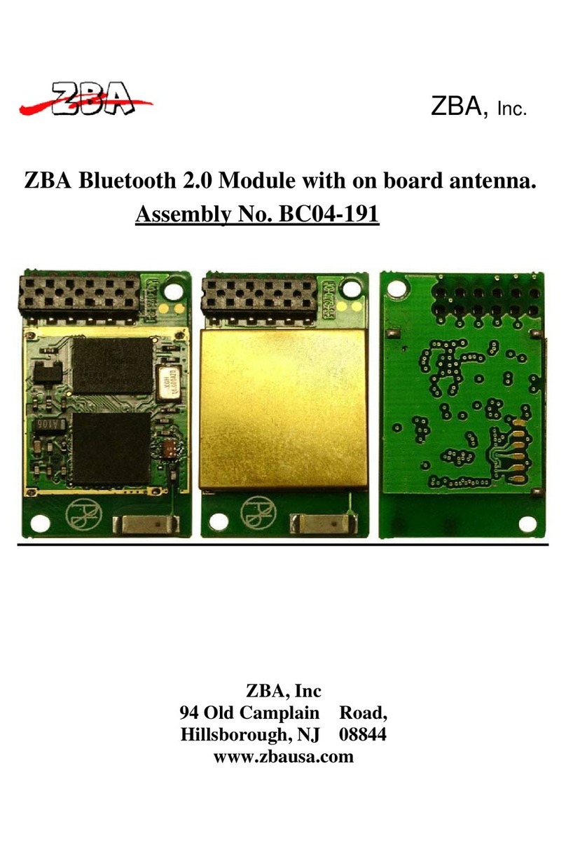
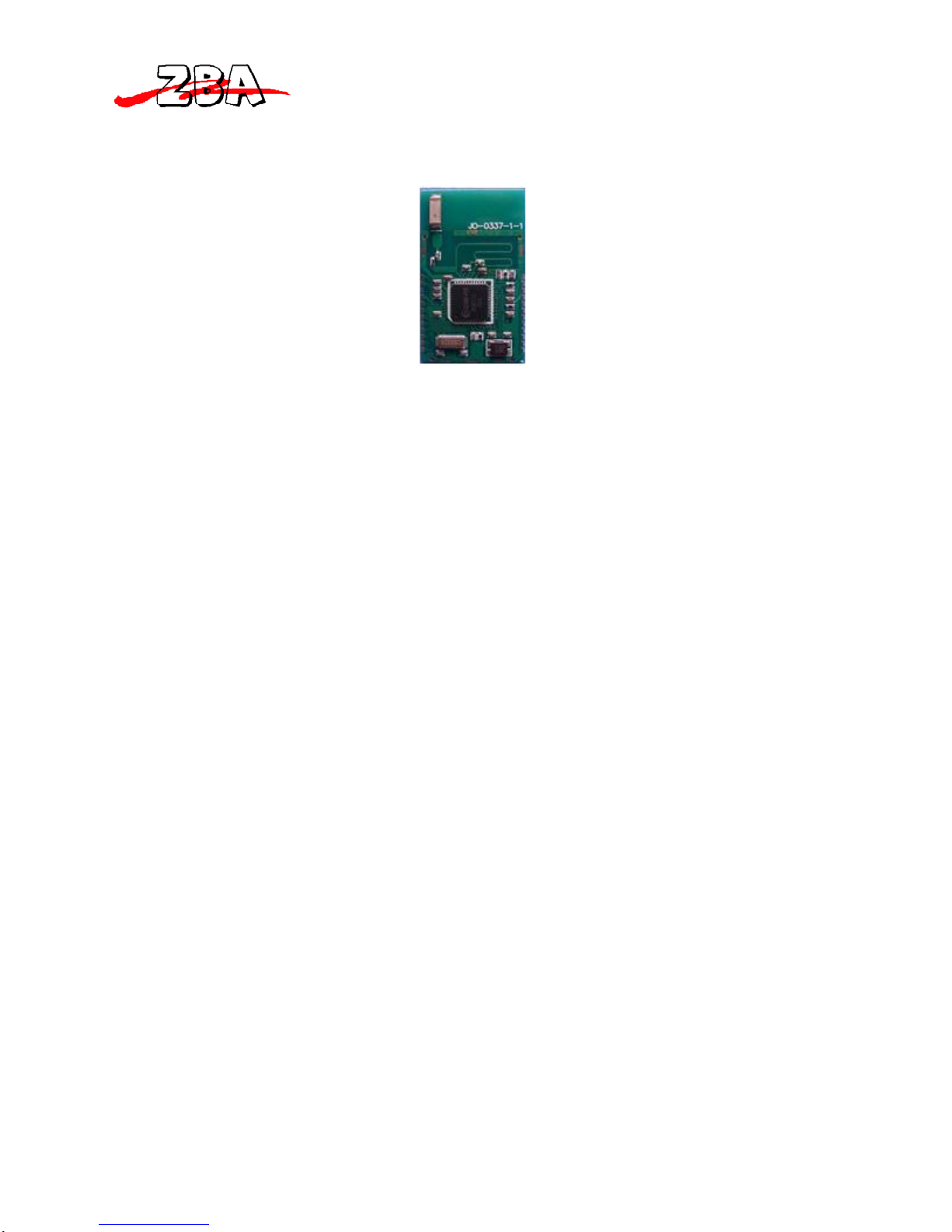
ZBA ZZB88-441S User manual

ZBA Inc.
ZBA, Inc.
94 Old Camplain Road Hillsborough, NJ 08844
Ph: 908-359-2070 Fax: 908-595-0909
Web: http://www.zbausa.com/
ZIGBEE Module
with on-board antenna
PN: ZZB88-441S
User Manual
Version: 1.0_20090622
PCB: JO-0337-1-1

ZBA Inc.
ZBA, Inc.
94 Old Camplain Road Hillsborough, NJ 08844
Ph: 908-359-2070 Fax: 908-595-0909
Web: http://www.zbausa.com/
Table of Contents
1Document Status ................................................................................................................................... 4
2Introduction........................................................................................................................................... 4
3Features................................................................................................................................................. 5
4Product performance............................................................................................................................. 5
4.1.1Low power consumption....................................................................................................... 5
4.1.2Network self-organization, self-healing ability..................................................................... 5
4.1.3Network capacity .................................................................................................................. 5
5Technical Specifications ....................................................................................................................... 7
5.1Absolute Max Ratings................................................................................................................... 7
5.2Electrical Description.................................................................................................................... 7
5.2.1Recommended operating voltage.......................................................................................... 7
5.3Electrical Specifications................................................................................................................ 8
5.3.1Current Consumption............................................................................................................ 8
5.4General Characteristics ................................................................................................................. 8
5.4.1Wake-Up and Timing............................................................................................................8
5.5RF Receive Section....................................................................................................................... 9
5.5.1RF Receive Parameters .........................................................................................................9
5.5.2RF Transmit Section ........................................................................................................... 10
5.6Analog to Digital Converter........................................................................................................ 10
6Hardware Interface Specification........................................................................................................ 11
6.1Module Pin-out ........................................................................................................................... 12
6.2Recommended PCB layout ......................................................................................................... 13
7Functional Interface Specification ...................................................................................................... 14
7.1Mode switch port ........................................................................................................................ 14
7.2Indicator ...................................................................................................................................... 14
7.3Data Interface.............................................................................................................................. 15
7.4Configuration Interface ............................................................................................................... 16
8The UART .......................................................................................................................................... 17
9Module Configuration Commands...................................................................................................... 18
9.1Instruction 1: Test command....................................................................................................... 18
9.2Instruction 2: check the version number ..................................................................................... 18
9.3Instruction 3: Set / Query the baud rate ...................................................................................... 18
9.4Instruction 4: Set / Query flowcontrol mode............................................................................... 18
9.5Instruction 5: Set / query the serial data bit.................................................................................18
9.6Instruction 6: set / check the serial port stop bits........................................................................ 18
9.7Instruction 7: set / query port parity............................................................................................ 19
9.8Instruction 8: Set / Query the device type................................................................................... 19
9.9Instruction 9: Set / query the network ID.................................................................................... 19
9.10Command 10: Set / query the communication channel .............................................................. 19
9.11Command 11: Set / query the data transmission mode ............................................................... 20
9.12Command12: Restore default settings ........................................................................................ 20
9.13Command 13: Query MAC address of the local module............................................................ 20
10Point-to-point mode Data specification .............................................................................................. 21
10.1Overview of the data packet format (point -to-point) ................................................................. 21
10.2Additional AT command request (0x00) & Response (0x01) Packet......................................... 21

ZBA Inc.
ZBA, Inc.
94 Old Camplain Road Hillsborough, NJ 08844
Ph: 908-359-2070 Fax: 908-595-0909
Web: http://www.zbausa.com/
10.3Instruction 1: MAC address of the local inquiry......................................................................... 22
10.4Instruction 2: Query a short address local network..................................................................... 22
10.5Instruction 3: MAC address of the remote query........................................................................ 22
10.6Instruction 4: Query remote short address .................................................................................. 23
10.7Instruction 5: parent and child nodes query node ....................................................................... 23
10.8Instruction 6: check the signal with the parent and child nodes.................................................. 23
10.9Instruction 7: check the signal with the surrounding nodes........................................................23
10.10Data Packet (0x10).................................................................................................................. 23
10.11Packet response (0x20) ........................................................................................................... 24
11Mounting Recommendations .............................................................................................................. 25
11.1Recommended Module Locations for On-Board Antenna ......................................................... 25
12Ordering Information .......................................................................................................................... 26
13Operational Notes ............................................................................................................................... 27
Table of Figures
Figure 5-1 Pin out of the module ............................................................................................................... 12
Figure 5-2 Recommended PCB layout ...................................................................................................... 13
Figure 6-1 Table of Mode switch port function......................................................................................... 14
Figure 6-2 Table of Indicator LED function.............................................................................................. 15
Figure 6-3 Table of default communication parameters ............................................................................ 15
Figure 6-4 Table of command communication parameters ....................................................................... 16
Figure 7-1 Diagram of the UART four (4) wire +ground interface:......................................................... 17
Figure 10-1 Side view of Zigbee module mounting recommendations .................................................... 25
Figure 10-2 Top view of Zigbee module mounting recommendations..................................................... 25
Figure 10-3 Typical Lead-Free Re-flow Solder Profile............................................................................ 26
Disclaimer:
No part of this document may be copied or reproduced in any form or by any means, or transferred to any third
party, without the prior written consent of an authorized representative of ZBA, Inc. (“ZBA”). The information in
this document is subject to change without notice. ZBA assumes no responsibility for any errors or omissions that
may appear in this document, and disclaims responsibility for any consequences resulting from the use of the
information set forth herein. ZBA makes no commitments to update or to keep current information contained in this
document. The products listed in this document are not suitable for use in applications such as, but not limited to,
aircraft control systems, aerospace equipment, submarine cables, nuclear reactor control systems and life support
systems. Moreover, ZBA does not recommend or approve the use of any of its products in life support devices or
systems or in any application where failure could result in injury or death. If a customer wishes to use ZBA products
in applications not intended by ZBA, said customer must contact an authorized ZBA representative to determine
ZBA’s willingness to support a given application. The information set forth in this document does not convey any
license under the copyrights, patent rights, trademarks or other intellectual property rights claimed and owned by
owned by ZBA. The information set forth in this document is considered to be “Proprietary” and “Confidential”
property
ALL PRODUCTS SOLD BY ZBA ARE COVERED BY THE PROVISIONS APPEARING IN ZBA’S TERMS
AND CONDITIONS OF SALE ONLY, INCLUDING THE LIMITATIONS OF LIABILITY, WARRANTY AND
INFRINGEMENT PROVISIONS. ZBA MAKES NO WARRANTIES OF ANY KIND, EXPRESS, STATUTORY,
IMPLIED OR OTHERWISE, REGARDING INFORMATION SET FORTH HEREIN OR REGARDING THE
FREEDOM OF THE DESCRIBED PRODUCTS FROM INTELLECTUAL PROPERTY INFRINGEMENT, AND
EXPRESSLY DISCLAIMS ANY SUCH WARRANTIES INCLUDING WITHOUT LIMITATION ANY
EXPRESS, STATUTORY OR IMPLIED WARRANTIES OF MERCHANTABILITY OR FITNESS FOR A
PARTICULAR PURPOSE.
ZBA Inc.
ZBA, Inc.
94 Old Camplain Road Hillsborough, NJ 08844
Ph: 908-359-2070 Fax: 908-595-0909
Web: http://www.zbausa.com/
1 Document Status
Date Comments
December 2010 First draft
To make a request for change, correction, additions or information on references, please
contact:
ZBA, Inc.
94 Old Camplain Road
Hillsborough, NJ 08844
Phone: 908-359-2070
Fax 908-595-0909
E-mail: [email protected]
Website : http://www.zbausa.com
2 Introduction
This highly integrated wireless communication module, embeds all of the necessary
components to perform a virtual plug and play function for ZIGBBE RF transceivers.
The module contains many of the necessary features required to built a reliable RF
communication network such as;, anti-interference ability, support for multiple network
topologies including self healing features, point to point, or point to multipoint
configuration which can be composed as star, tree, mesh tree network structure and of
course low power modes. .
The module is divided into a center coordinator, routers and end nodes, these three
distinct modes of operation provide the user with the option for different network
Structures that can be optimized for the particular application. The center of the network
is the coordinator node which is responsible for launching the network’s organization,
network maintenance and management, The data router function built-into the device,
which is responsible for transferring the data within the Zigbee network to the
coordinator and eventually to the host. The terminal nodes are typically at the end of the
network and typically perform the sensing and data acquisition function.
The coordinator, routers and end nodes configured by software commands. .

ZBA Inc.
ZBA, Inc.
94 Old Camplain Road Hillsborough, NJ 08844
Ph: 908-359-2070 Fax: 908-595-0909
Web: http://www.zbausa.com/
3 Features
•Surface mount module with ceramic on-board antenna
•Miniature module solution
•8KB of data memory
•Operating Frequency Band 2.40 GHz~2.48GHz unlicensed ISM Band
•IEEE 802.15.4 & ZigBee compliant
•Based upon the TI family of Zigbee SOC
•Multiple network topologies include MESH, Star, and point to point
•Large Network capacity
•Self-healing network. topology
•Low power consumption
•Sleep current (with active sleep timer) 2.8µA at 2.7V to 3.6V
•Easily configurable into different modes
•Broadcast, MASTER/SLAVE and point to point mode
•Royalty–free software
•Eliminate the need for complex RF Design and evaluation
•Easy to use AT command set for configuration control
•Class 2 type Output Power
•Precision Crystal oscillator on-board
•Industrial temperature range (-20 to +70°C)
4 Product performance
4.1.1 Low power consumption
This module can be configured in a variety of energy-saving modes, in which it is possible to
have a fully operational system run for more than 6 months on two AA batteries.
4.1.2 Network self-organization, self-healing ability
The Network configuration features of this module will allow the self-organizing of the network
without human intervention. The network’s nodes can sense the presence of other nodes and
determine the connection between composition and structure of the network;
The self-healing function can change the order in which data traverses through the network to
compensate for a change in node position, or node failures, etc. Low cost
This Zigbee module operates in the unlicensed ISM band at 2.40 GHz~2.48GHz and comes with
royalty-free firmware thereby yielding an extremely low cost system solution.
4.1.3 Network capacity
The specification for Zigbee network does allow for up to a maximum of 65,534 nodes in the
particular network. The Zigbee module can be configured to communicate via a standard serial

ZBA Inc.
ZBA, Inc.
94 Old Camplain Road Hillsborough, NJ 08844
Ph: 908-359-2070 Fax: 908-595-0909
Web: http://www.zbausa.com/
data (RS232 data) via the UART interface, and the firmware will allow you to transmit broadcast
messages to the other devices in the network. Any module in the network can be queried from the
coordinator to determine it operational mode and its relative position within the network.

ZBA Inc.
ZBA, Inc.
94 Old Camplain Road Hillsborough, NJ 08844
Ph: 908-359-2070 Fax: 908-595-0909
Web: http://www.zbausa.com/
5 Technical Specifications
5.1 Absolute Max Ratings
Paramete
r
Min Max Units Condition
Supply voltage –0.3 3.9 VAll supply pins must have the same voltage
Voltage on any
digital pin –0.3 VDD+0.3,
max 3.9
V
Voltage on the 1.8V
pins (pin no.
22, 25-40 and 42)
–0.3 2.0
V
Input RF level 10 dBm
Storage temperature –50 150 °C Device not programmed
ESD
<500 V
V On RF pads (RF_P, RF_N, AVDD_RF1,
and AVDD_RF2), according to Human
Body Model, JEDEC STD 22, method A114
700 V V All other pads, according to Human Body
Model, JEDEC STD 22, method A114
200 V V According to Charged Device Model,
JEDEC STD 22, method C101
5.2 Electrical Description
5.2.1 Recommended operating voltage
Name Min
Type Max Units
Vcc-In 2.0 3.0 3.6 V
Vcr-Filter 1.75 1.8 1.85 V
The actual electrical characteristics (rated operating current) Vcc = Vcc-In
Name Min Type Max Unit
Logic“0”Input Voltage 0 0.7 0.9 V
Logic“1”Input Voltage Vcc-0.7 Vcc Vcc V
Logic“0”Output Voltage (note1) 0 0 0.25 V
Logic“1”Output Voltage (note1) Vcc-0.25 Vcc Vcc V
Logic“0”Input Current (note2) NA -1 -1 uA
Logic“1”Input Current (note3) NA 1 1 uA
I/O pin pull-up and pull-down resistor I 17 20 23 K
note1: For 4mA output current on all pins except P1_0 and P1_1 which are rated to 20mA;
note2: Input equals 0V;
note3: Input equals Vcc;

ZBA Inc.
ZBA, Inc.
94 Old Camplain Road Hillsborough, NJ 08844
Ph: 908-359-2070 Fax: 908-595-0909
Web: http://www.zbausa.com/
5.3 Electrical Specifications
5.3.1 Current Consumption
Measured with Ta=25°C and VDD=3.0V unless stated otherwise.
Operational mode
Current Unit Measurement condition
MCU Active and RX
Mode
26.7 mA MCU running at full speed (32MHz), 32MHz XOSC running, radio in RX
mode, -50 dBm input power. No peripherals active. Code run with Cache hit.
MCU Active and TX
Mode, 0dBm
26.9 mA MCU running at full speed (32MHz), 32MHz XOSC running, radio in TX
mode, 0dBm output power. No peripherals active. Code run with Cache hit.
MCU Active Mode, 32
MHz
9.5 mA MCU running at full speed (32MHz), 32MHz XOSC running. No radio or
peripherals active. Code run with Cache hit.
Power mode 1 190 µA Digital regulator on, High frequency RCOSC and crystal oscillator off.
32.768 kHz XOSC, POR and ST active.
RAM retention.
Power mode 2 0.5 0µA Digital regulator off, High frequency RCOSC and crystal oscillator off.
32.768 kHz XOSC, POR and ST active.
RAM retention.
Power mode 3 0.3 µA No clocks. RAM retention. POR active.
5.4 General Characteristics
5.4.1 Wake-Up and Timing
Measured with Ta = 25 ° C and VDD = 3.0V unless stated otherwise.
Paramete
r
Min Typ Max Unit Condition/Note
Power mode 1 mode 0 4.1 µS Digital regulator on, High frequency RCOSC and crystal oscillator
off. Startup of High frequency RCOSC.
Power mode 2 or 3
mode 0
89.2 µS Digital regulator off, High frequency RCOSC and crystal
oscillator off. Startup of regulator and High frequency RCOSC.
Active TX or RX
Active TX or RX
32MHz XOSC initially
OFF.
Voltage regulator initially
OFF
525 µS Time from enabling radio part in power mode 0, until TX or RX
starts. Includes start-up of voltage regulator and crystal oscillator
in parallel. Crystal ESR=16.
Active TX or RX
Voltage regulator initially
OFF
320 µS Time from enabling radio part in power mode 0, until TX or RX
starts. Includes start-up of voltage regulator.
Active RX or TX 192 µS Radio part already enabled...
Time until RX or TX starts.

ZBA Inc.
ZBA, Inc.
94 Old Camplain Road Hillsborough, NJ 08844
Ph: 908-359-2070 Fax: 908-595-0909
Web: http://www.zbausa.com/
5.5 RF Receive Section
5.5.1 RF Receive Parameters
Measured with TA = 25 ° C and VDD = 3.0V unless stated otherwise.
Paramete
r
Min Typ Max Unit
Condition/Note
Receiver sensitivity -91 dBm PER (packet error rate) = 1%, as specified by [1]
Measured in 50 single ended through a balun.
[1] requires –85 dBm
Saturation (maximum
input level)
10 dBm PER = 1%, as specified by [1]
Measured in 50Single ended through a balun.
[1] requires -20 dBm
Adjacent channel
rejection + 5 MHz
channel spacing
41 dB Wanted signal -88dBm, adjacent modulated channel at +5
MHz, PER = 1 %, as specified by [1].
[1] requires 0 dB
Adjacent channel
rejection - 5 MHz
channel spacing
30 dB Wanted signal -88dBm, adjacent modulated channel at -5
MHz, PER = 1 %, as specified by [1].
[1] requires 0 dB
Alternate channel
rejection + 10 MHz
channel spacing
55 dB Wanted signal -88dBm, adjacent modulated channel at +10
MHz, PER = 1 %, as specified by [1]
[1] requires 30 dB
Alternate channel
rejection - 10 MHz
channel spacing
53 dB Wanted signal -88dBm, adjacent modulated channel at -10
MHz, PER = 1 %, as specified by [1]
[1] requires 30 dB
Channel rejection
+ 15 MHz
- 15 MHz
55
53
dB
dB
Wanted signal @ -82 dBm. Undesired signal is an 802.15.4
modulated channel, stepped through all channels from 2405
to 2480 MHz. Signal level for PER = 1%. Values are
estimated.
Co-channel rejection -6 dB Wanted signal @ -82 dBm. Undesired signal is 802.15.4
modulated at the same frequency as the desired signal. Signal
level for PER = 1%.
Blocking /
Desensitization
+ 5 MHz from band edge
-42
dBm
Wanted signal 3 dB above the sensitivity level, CW jammer,
PER = 1%. Measured according to EN 300 440 class 2.
+ 10 MHz from band
edge
-45 dBm
+ 20 MHz from band
edge
-26 dBm
+ 50 MHz from band
edge
-22 dBm
- 5 MHz from band edge -31 dBm
- 10 MHz from band edge -36 dBm
- 20 MHz from band edge -24 dBm

ZBA Inc.
ZBA, Inc.
94 Old Camplain Road Hillsborough, NJ 08844
Ph: 908-359-2070 Fax: 908-595-0909
Web: http://www.zbausa.com/
- 50 MHz from band edge -25 dBm
Spurious emission Conducted measurement in a 50 single ended load.
Complies with EN 300 328, EN 300 440 class 2, FCC
CFR47, Part 15 and ARIB STD-T-66
30 – 1000 MHz -64 dBm
1 – 12.75 GHz -75 dBm
Frequency error tolerance ±140 ppm Difference between centre frequency of the received RF
signal and local oscillator frequency.
[1] requires minimum 80 ppm
Symbol rate error
tolerance
±900 ppm Difference between incoming symbol rate and the internally
generated symbol rate [1] requires minimum 80 ppm
5.5.2 RF Transmit Section
Measured with TA = 25 ° C and VDD = 3.0V unless stated otherwise.
Paramete
r
Min Typ
Max Unit Condition/Note
Nominal output power 0 dBm Delivered to a single ended 50load through a balun and
output power control set to 0x5F (TXCTRLL).
[1] requires minimum –3 dBm
Programmable output
power range
25.8 dB The output power is programmable in 16 steps from
approximately –25.2 to 0.6 dBm...
Harmonics . Measurement conducted with 100 kHz resolution bandwidth
on spectrum analyzer and output power control set to 0x5F
(TXCTRLL). Output Delivered to a single ended 50load
through a balun.
2nd harmonic -50.7 dBm
3rd harmonic -55.8 dBm
4th harmonic -54.2 dBm
5th harmonic -53.4 dBm
Spurious emission Maximum output power.
The peak conducted spurious emission is -47dBm@192MHz
which is in an EN300440 restricted band limited to -54dBm.
30 - 1000 MHz -47 dBm
1– 12.75 GHz -43 dBm
1.8 – 1.9 GHz -58 dBm
5.15 – 5.3 GHz -56 dBm
Error Vector Magnitude
(EVM)
11 % Measured as defined by [1]
[1] Requires max. 35 %
Optimum load
impedance
115
+ j180
Differential impedance as seen from the RF-port (RF_P and
RF_N) towards the antenna...
5.6 Analog to Digital Converter

ZBA Inc.
ZBA, Inc.
94 Old Camplain Road Hillsborough, NJ 08844
Ph: 908-359-2070 Fax: 908-595-0909
Web: http://www.zbausa.com/
Measured with TA = 25 ° C, VDD = 3.0V.Preliminary characterized parameters.
Paramete
r
Min
Typ Max Unit
Condition/Note
Input voltage 0 AVDD V AVDD is voltage on AVDD_SOC
pin
External reference voltage 0 AVDD V AVDD is voltage on AVDD_SOC
pin
External reference voltage differential 0 AVDD V AVDD is voltage on AVDD_SOC
pin
Input resistance, ADC single-ended input 167 kAIN0 to AIN7 selected as ADC input
Input resistance, ADC differential input2 TBD
Input resistance, single-ended reference 49 kAIN7 selected as external reference
input
Input resistance, differential reference1 TBD
Effective number of bits (ENOB)2 5.5
7.3
9.0
10.5
Bits 8-bits setting.
10-bits setting.
12-bits setting.
14-bits setting.
Effective number of bits (ENOB)
Differential input1 E
TBD
Offset1 TBD LSB
Conversion time 20
36
68
132
µS
µS
µS
µS
8-bits setting. 8-bits setting.
10-bits setting. 10-bits setting.
12-bits setting. 12-bits setting.
14-bits setting. 14-bits setting.
Differential nonlinearity (DNL)3 ± 0.14 1.0 LSB 8-bits setting. 8-bits setting.
Integral nonlinearity (INL) 2 ±0.5 3.4 LSB 8-bits setting. 8-bits setting.
SINAD2
(Sine input signal
frequency 1 Hz and 1 kHz)
34
46
56
65
dB
dB
dB
dB
8-bits setting.
10-bits setting.
12-bits setting.
14-bits setting.
ADC Characteristics
1. Only for devices with Chip Version register, CHVER.VERSION equal to 0x02 or greater
2. Not characterized for this data sheet revision.
3. Single-ended input signal and AVDD used as reference. Sine input, tested at frequencies 1 Hz
and 1 kHz
6 Hardware Interface Specification

ZBA Inc.
ZBA, Inc.
94 Old Camplain Road Hillsborough, NJ 08844
Ph: 908-359-2070 Fax: 908-595-0909
Web: http://www.zbausa.com/
6.1 Module Pin-out
Figure 6-1 Pin out of the module

ZBA Inc.
ZBA, Inc.
94 Old Camplain Road Hillsborough, NJ 08844
Ph: 908-359-2070 Fax: 908-595-0909
Web: http://www.zbausa.com/
6.2 Recommended PCB layout
Figure 6-2 Recommended PCB layout
Pin List
Pin No. Function Type Description
1P22 Digital I/O
2P21 Digital I/O
3GND Ground System ground.
4Vcc-In Power Input 2.0V-3.6V digital power supply for digital I/O.
5P20 Digital I/O
6P17 Digital I/O
7P16 Digital I/O
8P15 Digital I/O
9P14 Digital I/O
10 P13 Digital I/O
11 P12 Digital I/O
12 P11 Digital I/O Network LED (20mA drive capability)
Antenna
area
Dimensions in mm

ZBA Inc.
ZBA, Inc.
94 Old Camplain Road Hillsborough, NJ 08844
Ph: 908-359-2070 Fax: 908-595-0909
Web: http://www.zbausa.com/
13 P10 Digital I/O Indicator LED Drive (20mA capability)
14 RST Reset, active low.
15 P00 Digital I/O
16 P01 Digital I/O Input for Mode switching functions hi=configuration mode, low-running
mode
17 P02 Digital I/O
18 P03 Digital I/O
19 P04 Digital I/O
20 P05 Digital I/O
21 P06 Digital I/O
22 P07 Digital I/O
23 Vcr-Filter Power
Output
1.8V Voltage regulator power supply output. Only intended for supplying
the analog 1.8V part.
24 GND Ground System ground.
7 Functional Interface Specification
7.1 Mode switch port
Input/ output port PIO_01 is configured as a mode switching port. When the module is controlled by an
external microprocessor switching this pin will allow the user to switch between the normal operation
running mode and the command mode. When the mode pin is set to a logic low level “0” the module is in
the active, operational mode. When the mode pin is set to logic high state “1” then the module is in
configuration parameters. See table below for a summary.
Mode pin State Operational state
Logic low Zigbee network operational MODE
Logic high Command mode
Figure 7-1 Table of Mode switch port function
7.2 Indicator
This Zigbee wireless module has allocated two PIO to operate as status LED indicators. The
instructions were operational mode (pin 13 ÆP10), and the network indication (pin 12 ÆP11), the two (2)
LEDs indicate status and are described in the following table:

ZBA Inc.
ZBA, Inc.
94 Old Camplain Road Hillsborough, NJ 08844
Ph: 908-359-2070 Fax: 908-595-0909
Web: http://www.zbausa.com/
Indicator LED status Description
Operating
instructions
(port =P10)
LED indicator will
flash once each second
The system operating normally
LED indicator is
illuminated constantly
The module is in the configuration set-
up mode.
LED indicator is Off System is not running, indicating a
power or system failure
Network
instructions
(port = P11)
LED indicator is Off Central node
(coordinator)
A successful
network has been
created
Routing node The node has Join
the network
Terminal node The node has Join
the network
Always Not connected to the network
Figure 7-2 Table of Indicator LED function
7.3 Data Interface
The Zigbee module can be operated via communication to a standard UART function with either a four (4)
wire + ground UART connection (TX, RX, RTS, CTS, GND ) or a two (2) wire +ground UART
connections (TX, RX, GND)
The default data interface parameters:
Serial port parameters Default
Baud Rate 9600
Parity NONE
Data bits 8
Stop bit 1
Figure 7-3 Table of default communication parameters

ZBA Inc.
ZBA, Inc.
94 Old Camplain Road Hillsborough, NJ 08844
Ph: 908-359-2070 Fax: 908-595-0909
Web: http://www.zbausa.com/
7.4 Configuration Interface
When the ZIGBEE wireless communication module MODE switch pin (PIO_01) pin is
connected high, the system enters the command mode; low on this pin will shift the module’s
operating mode to the operational mode. .
The command mode will only accept command at a fixed communication setting as outlined in the table
below.
Serial Port
parameters Fixed comm.
parameters
Baud Rate 9600
Parity NONE
Data bits 8
Stop bit 1
Figure 7-4 Table of command communication parameters

ZBA Inc.
ZBA, Inc.
94 Old Camplain Road Hillsborough, NJ 08844
Ph: 908-359-2070 Fax: 908-595-0909
Web: http://www.zbausa.com/
8 The UART
The module provides four-wire+ Ground serial asynchronous communication interface;
The following diagram shows the TXD, RXD, CTS, RTS signals for the UART and the direction of the
data flow. The voltage levels of the UART are low= 0 Volts and Hi = Vdd (3.3Volts). For two (2) wire +
Ground operation do not connect CTS and RTS.
Figure 8-1 Diagram of the UART four (4) wire +ground interface:
Ground
Direction of signals

ZBA Inc.
ZBA, Inc.
94 Old Camplain Road Hillsborough, NJ 08844
Ph: 908-359-2070 Fax: 908-595-0909
Web: http://www.zbausa.com/
9 Module Configuration Commands
9.1 Instruction 1: Test command
Command Response Parameters
AT\r\n OK No
9.2 Instruction 2: check the version number
Command Response Parameters
AT+VERSION? \r\n OK
\ r \ n + VERSION: <Para1> \ r \ n
Para1: the version number
9.3 Instruction 3: Set / Query the baud rate
Command Response Parameters
AT+BAUD=<
Para1>\r\n
OK Para1: baud rate (1200, 2400, 4800, 9600, 19200,
38400, 57600, 115200, 230400)
Default:9600
AT+BAUD?\r\n OK
\r\n +BAUD :<Para1>\r\n
Note: The communication parameters used during the communication mode is fixed at 9600 N 8 1
9.4 Instruction 4: Set / Query flowcontrol mode
Command Response Parameters
AT+ FLOWCONTROL=<Para1>\r\n OK <Para1> :<Para1>:
0: No flow control
1: The hardware flow control
Default: 1
AT+ FLOWCONTROL?\r\n OK
\r\n +FLOWCONTROL:
<Para1>\r\n \
9.5 Instruction 5: Set / query the serial data bit
Command Response Parameters
AT+ DATABIT=<Para1>\r\n OK <Para1> :<Para1>:
8: 8
9: 9
Default: 8
AT+ DATABIT?\r\n OK
\r\n +DATABIT :<Para1>\r\n \
9.6 Instruction 6: set / check the serial port stop bits

ZBA Inc.
ZBA, Inc.
94 Old Camplain Road Hillsborough, NJ 08844
Ph: 908-359-2070 Fax: 908-595-0909
Web: http://www.zbausa.com/
Command Response Parameters
AT+ STOPBIT=<Para1>\r\n OK <Para1> :
1: 1 Stop bit
2: 2 Stop bits
Default: 1stop bit
AT+ STOPBIT?\r\n OK
\r\n +STOPBIT: <Para1>\r\n
9.7 Instruction 7: set / query port parity
Command Response Parameters
AT+ VERIFYBIT=<Para1>\r\n OK <Para1> :
0: no parity
1: odd parity
2: even parity
Default: 0
AT+ VERIFYBIT?\r\n OK
\r\n +VERIFYBIT :<Para1>\r\n
9.8 Instruction 8: Set / Query the device type
Command Response Parameters
AT+ ROLE=<Para1>\r\n OK <Para1>:
0: The central node
1: The routing node
2: The terminal node
Default: 1
AT+ ROLE?\r\n OK
\r\n +ROLE :<Para1>\r\n
9.9 Instruction 9: Set / query the network ID
Command Response
P
arameters
AT+ PANID=<Para1>\r\n OK <Para1> :
0000 ~ 3FFF
Default:
AT+ PANID\r\n OK
\r\n +PANID :<Para1>\r\n \
9.10 Command 10: Set / query the communication channel
Command Response Parameters
AT+ CHANNEL=<Para1>\r\n OK <Para1> :
0 ~ 15
Default:
AT+ CHANNEL\r\n OK
\r\n +CHANNEL :<Para1>\r\n
Communication channel Channel / Frequency Remarks
0~15 00/ 2.405GHz It is recommended to use channels 4, 9, 14, 15 to avoid
interference with any local WIFI.

ZBA Inc.
ZBA, Inc.
94 Old Camplain Road Hillsborough, NJ 08844
Ph: 908-359-2070 Fax: 908-595-0909
Web: http://www.zbausa.com/
01/ 2.410 GHz
02/ 2.415 GHz
03/ 2.420 GHz
04/ 2.425GHz
05/ 2.430 GHz
06/ 2.435GHz
07/ 2.440 GHz
08/ 2.445GHz
09/ 2.450 GHz
10/ 2.455GHz
11/ 2.460 GHz
12/ 2.465GHz
13/ 2.470 GHz
14/ 2.475GHz
15/ 2.480 GHz
9.11 Command 11: Set / query the data transmission mode
Command Response Parameters
AT+ SENDTYPE =<Para1>\r\n OK <Para1> :
0: Broadcast Mode
1: Master-slave mode
2: Point-to-point mode
AT+ SENDTYPE \r\n OK
\r\n +SENDTYPE :<Para1>\r\n
0) Broadcast Mode: When operating the broadcast mode; each of the nodes in the network will be able to
receive the broadcast message.
1) Master-slave mode: When operating in the Master Slave mode the serial data is sent to the central
coordinator. The other nodes in the network simply act as a pass through and do not actually receive the
serial data. The Serial Data terminates at the Central coordinator.
2) Point to point Mode: When operating in point to point mode: the node must format the data as outlined
below, such that the serial transmit and receive data are properly interpreted. (See below for the specific
point to point data format )
9.12 Command12: Restore default settings
Command Response Parameters
AT+RESET\r\n OK No
9.13 Command 13: Query MAC address of the local module
Command Response Parameters
AT+LEXTADDR?\r \r\nOK\r\n
\r\n+LEXTADDR:<eaddr>\r\n eaddr: 64-bit extended MAC address
Table of contents
Other ZBA Control Unit manuals
Popular Control Unit manuals by other brands

SPI Lasers
SPI Lasers redPOWER FVCU Instructions for use

Vaisala
Vaisala HMM30C operating manual

CommScope
CommScope SYSTIMAX 360 iPatch 360-iP-1100-E-GS3-1U-24 installation instructions

Maxon
Maxon ESCON 50/4 EC-S Hardware reference

GF Piping Systems
GF Piping Systems NeoFlow operating instructions

Move
Move MAMWLE Series manual