Zida CreateBXi-ATX User manual

USER’S
MANUAL
More compatible, more functional and more competitive. Excellent quali-
ty and faster response.
Supporting Intel PENTIUM III
®
, PENTIUM II
®or Celeron
®
Processors, Accelerated Graphics Port, Hardware Monitor
(Optional), Pd Bus Master IDE, SDRAM.
Quality, Performance Mainboards

contents
Table Of Contents
Overview. . . . . . . . . . . . . . . . . . . . . . . . . . . . . . . . . . . . .5
Fast start installation. . . . . . . . . . . . . . . . . . . . . . . . . . . . .6
Checking the Package Contents. . . . . . . . . . . . . . . . . . . .7
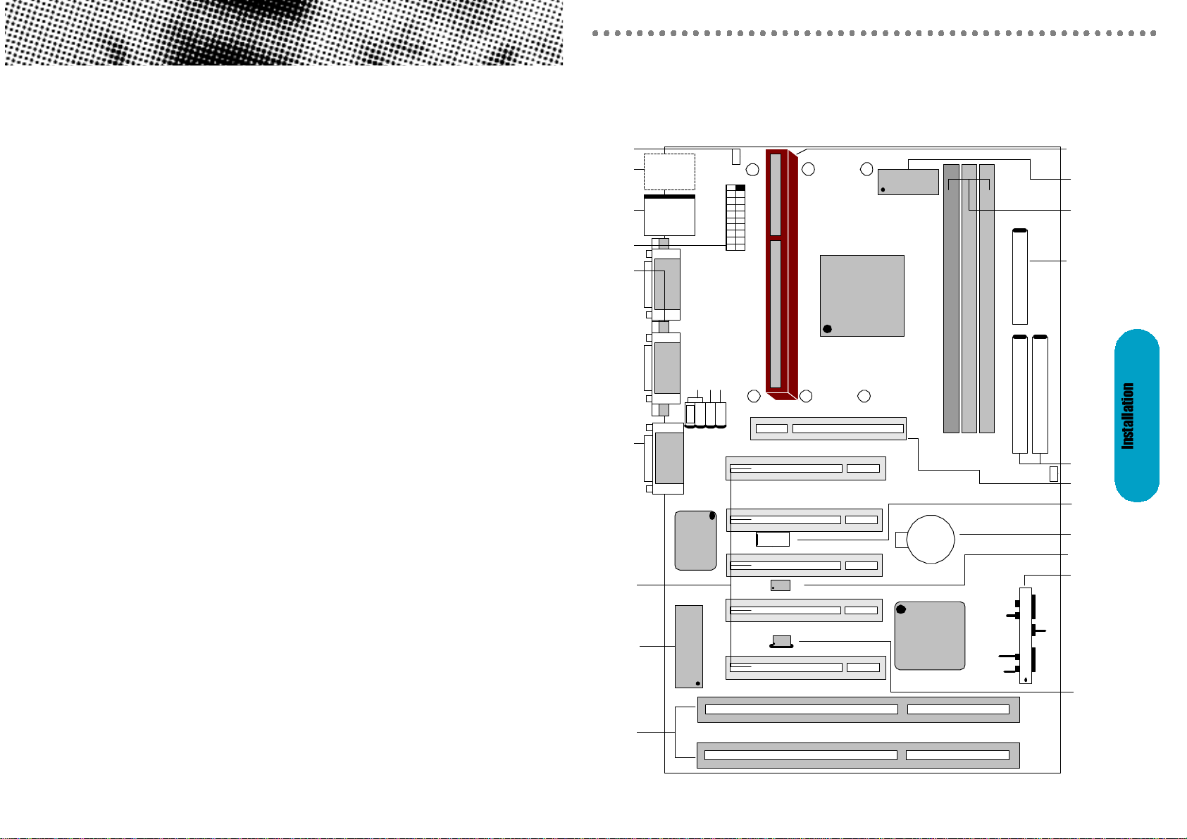
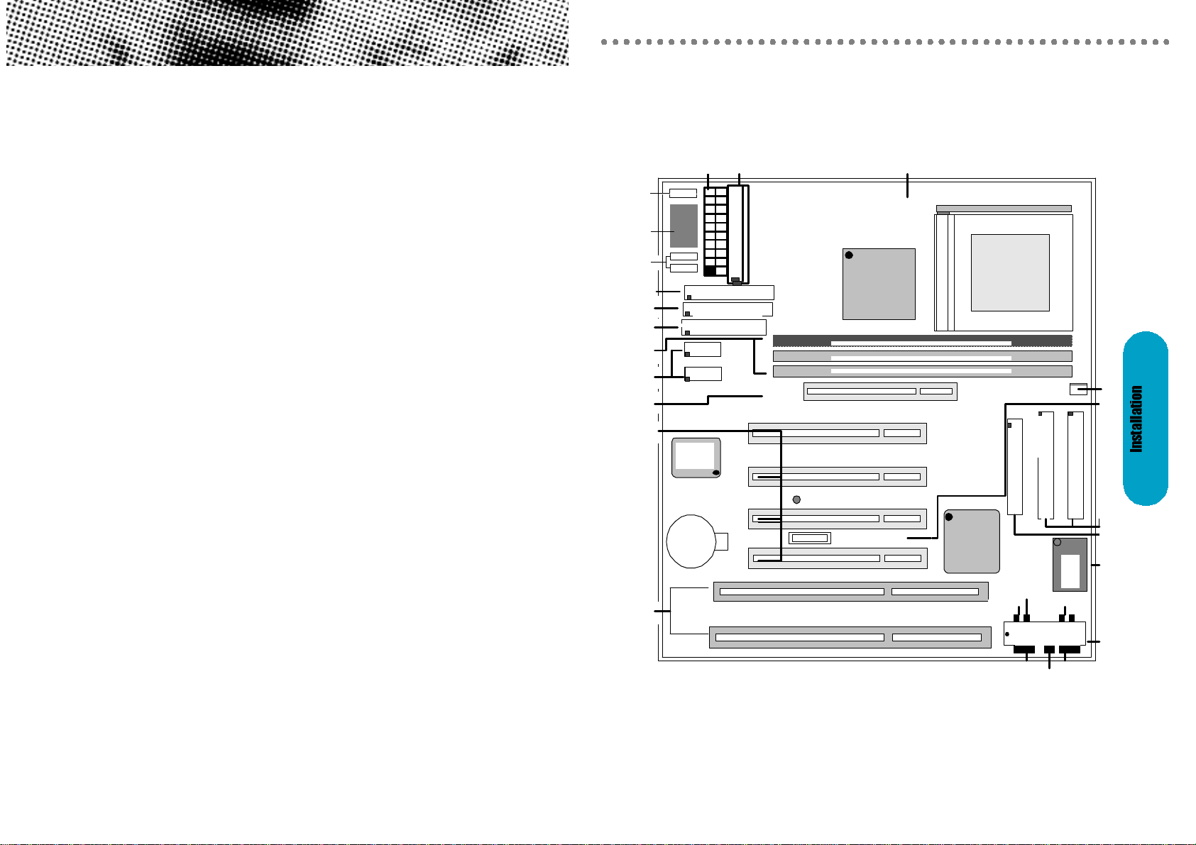
Mainboard diagram. . . . . . . . . . . . . . . . . . . . . . . . . . . . . .9
6 quick steps. . . . . . . . . . . . . . . . . . . . . . . . . . . . . . . . .16
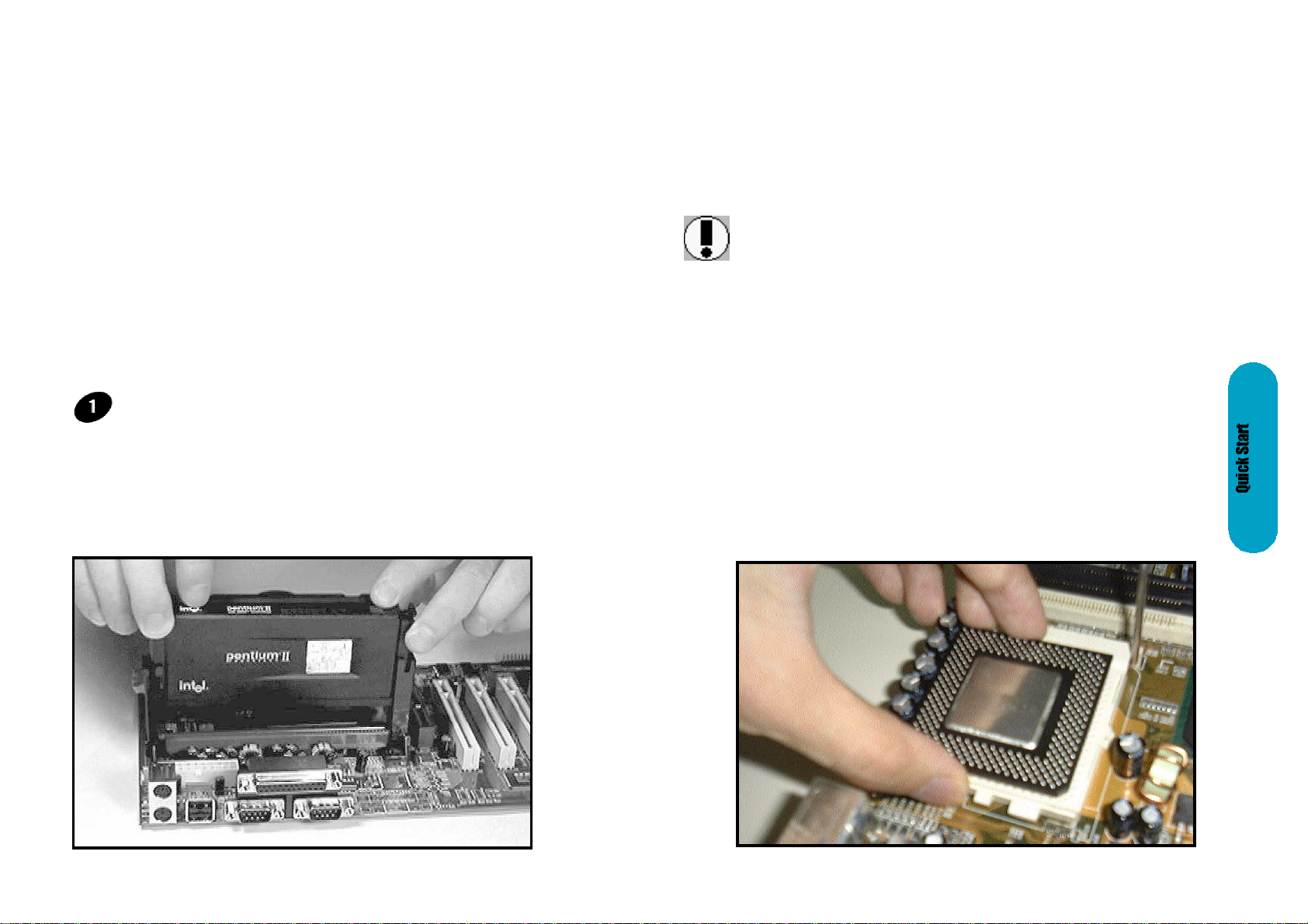
Installing the CPU. . . . . . . . . . . . . . . . . . . . . . . . . . . . . .16
Installing RAM. . . . . . . . . . . . . . . . . . . . . . . . . . . . . . . .18
Attaching power. . . . . . . . . . . . . . . . . . . . . . . . . . . . . . .19
Floppy Drive connector. . . . . . . . . . . . . . . . . . . . . . . . . .20
IDE connector. . . . . . . . . . . . . . . . . . . . . . . . . . . . . . . . .20
Mounting Mainboard to chassis. . . . . . . . . . . . . . . . . . . .21
Installing Video Card. . . . . . . . . . . . . . . . . . . . . . . . . . . .22
Installing Add-on Boards. . . . . . . . . . . . . . . . . . . . . . . . .22
Bios set-up. . . . . . . . . . . . . . . . . . . . . . . . . . . . . . . . . . .24
Glossary. . . . . . . . . . . . . . . . . . . . . . . . . . . . . . . . . . . . .46
MainboardUser'sManualPage 3
No part of this manual, including the products and software described in it, may be
reproduced, transmitted, transcribed, stored in a retrieval system, or translated into any
language in any form or by any means, except documentation kept by the purchaser for
backup purposes, without the express written permission of MANUFACTURER.
MANUFACTURER PROVIDES THIS MANUAL “AS IS” WITHOUT WARRANTY OF ANY
KIND, EITHER EXPRESS OR IMPLIED, INCLUDING BUT NOT LIMITED TO THE
IMPLIED WARRANTIES OR CONDITIONS OF MERCHANTABILITY OR FITNESS FOR
A PARTICULAR PURPOSE.
IN NO EVENT SHALL MANUFACTURER, ITS DIRECTORS, OFFICERS, EMPLOYEES
OR AGENTS BE LIABLE FOR ANY INDIRECT. SPECIAL, INCIDENTAL, OR
CONSEQUENTIAL DAMAGES (INCLUDING DAMAGES FOR LOSS OF PROFITS,
LOSS OF BUSINESS, LOSS OF USE OR DATA, INTERUPTION OF BUSINESS AND
THE LIKE), EVEN IF MANUFACTURER HAS BEEN ADVISED OF THE POSSIBILITY
OF SUCH DAMAGES ARISING FROM ANY DEFECT OR ERROR IN THlS MANUAL
OR PRODUCT.
Products and corporate names appearing in this manual may or may not be registered
trademarks or copyrights of their respective companies, and are used only for
identification or explanation and to the owners benefit, without intent to infringe
Intel, Pentium, Pentium II are registered trademark of Intel Corporation
VIA is a registered trademark of VIA Technologies, Incorporated
IBM, IBM PC, IBM PC/AT, PC-DOS, OS/2 and OS/2 WARP are registered trademarks
of International Business Machines Corporation.
Ms-DOS, Windows, Windows NT, Windows 98 and Windows 95 are registered
trademarks of Microsoft Corporation.
AMI BIOS is a product of American Megatrends, Inc.
AWARD BIOS is a product of Award Software Inc.
Third-party brands and names mentioned in this User’s Guide are the property of their
respective owners.
The product name and revision number are both printed on the board itself. Manual
revisions are released for each board design represented by the digit before and after
the period of the manual revision number. Manual updates are represented by the third
digit in the manual revision number.
SPECIFlCATlONS AND INFORMATION CONTAINED IN THIS MANUAL ARE
FURNISHED FOR INFORMATION USE ONLY, AND ARE SUBJECT TO CHANGE AT
ANY TIME WITHOUT NOTICE, AND SHOULD NOT BE CONSTURED AS A
COMMiTMENT BY MANUFACTURER. MANUFACTURER ASSUMES NO
RESPONSIBILITY OR LIABILITY FOR ANY ERRORS OR INACCURACIES THAT MAY
APPEAR IN THIS MANUAL, INCLUDING THE PRODUCTS AND SOFTWARE
DESCRIBED IN IT.
Copyright © 1999 Manufacturer All Rights Reserved.
Manual Revision:1.00
Release Date:April 1999
Part No: 90- CREATES1.00-00
Page 2MainboardUser'sManual

overview
Thank You for purchasing our High Performance PENTIUM III
®
PENTIUMII or CELERON
®Mainboard. Our advanced technology
mainboard is designed for processing speeds of 233MHz and
333MHz or above and is upgradeable for future processors.
The Intel Mainboard Utilizes Intel's PCI chipset and their IDE
Xcelerator provides an integrated Bus Mastering IDE controller with
two (2) high performance IDE interfaces for up to four (4)IDEdevices
(hard drives, or CD-ROM's). It's I/O controller integrates floppy drive
interface, two (2) FIFO serial ports, one (1) parallel port
and Consumer Infra Red compatible interface.
The VIA Mainboard utilizes VIA's PCI chipset. The VIA's PCI/ISA
IDE provides an integrated Bus Mastering IDE controller with two
high performance IDE interfaces for up to four IDE devices (such as
hard drives or CD-ROM). The integrated super I/O controller
integrates the standard PC I/O functions: floppy interface, two FIFO
serial ports, one EPP/ECP capable parallel port, and support for an
IrDA and Consumer Infra Red compatible interface.
This mainboard is designed to support the new graphic interface
standard, Accelerated Graphic Port (AGP), The AGP interface can
reach a theoretical ~532Mbytes/sec transfer rate for 3D graphics
data. On the other hand, the on-board 32-bit PCI local bus slots
allow a high bandwidth data path, which serves as a super highway,
for intensive data-movement such as networking. The BIOS support
PCI bridge user configuration, which allows for further expansion of
the system with PCI peripherals. Up to two 16-bit ISA slots allow this
board to be backward compatible with the older expansion card. A
total of six expansion slots may be populated with full length add-in
cards, since one PCI and ISA slot share the same chassis I/O panel.
This Mainboard is among our “Auto Jumper” Series that eliminates
the necessity for the user to be overwhelmed by jumper settings on
the Mainboard. It is capable of detecting the CPU brand and core
voltage, setting the appropriate CPU speed according to the
instructions from the user through the CMOS setup.
MainboardUser'sManualPage 5

Checking The Package Contents
Remove the items from the box and make sure you have the
following items before beginning. If you are missing any of the
items below please contact the representative for a replacement
part.
ATXBox Standard Package
1) Mainboard
2) IDE Hard Drive ribbon cable
3) Floppy Drive Ribbon Cable
4) CD-ROM
5) Users Guide
ATBox Standard Package
1) Mainboard
2) CD-ROM
3) Users Guide
Page6MainboardUser'sManual
fast start
installation
This section will aid you in quickly setting up your series
Mainboard, be sure to use caution to avoid personal injury and
damage to wiring due to sharp pins on connector's and printed
circuit assemblies, rough edges and corners and hot components.
Adhere to warnings regarding accessibility into ares designated
only for authorized Technicians.
Your Location Requirements Are:
• A sturdy, level surface for placement
• Space allowance around mainboard
• Room temperature 50 to 90.5 F10 to 325 C Relative
humidity 20/oc to 80
• A stable environment with no abrupt temperature or
humidity changes
• No exposure to chemicals or direct sunlight
• Line voltage and frequency not varying more than + or -1040
from the value stated on the package or nameplate (located on
the back, opposite the power plug)
Auto Jumper. This Mainboard is among our “Auto
Jumper” Series that eliminates the necessity for the user
to be Overwhelmed by jumper settings on the Mainboard.
It is capable of detecting the CPU brand and core voltage
setting the appropriate CPU speed according to the
instructions from the user through the CMOS setup.
MainboardUser'sManualPage7

MainboardUser'sManualPage9
BIOS
PCI 4
PCI 3
PCI 2
PCI 1
AGP
ISA 1
ISA 2
CPU SLOT
BOTTOM:
KEYBOARD
USB
COM2 PARALLEL COM1
TOP:
MOUSE
POWER
SOCKET
FLOPPY
SECONDARY IDE
PRIMARY IDE
CPU
FAN
J17
DIMM3
DIMM2
DIMM1
AUDIO
CONNECTOR
PCI 5
IDE2
IDE1
1Front Panel JP9
KEYLOCK EXTSMI SPEAKER
RESET
PWR .ON
IDE. LED
Hardware Monitor
GENESYS 520
Creative
Sound
Chipset
INFRARED
Wakeup-Link
S3
S2
S1
A
C
B
G
H
U
N
JM
Q
T
K
S
W
F
O
P
E
I
xz
FAN
J16
J28
J30
J34
J31
SB-Link
Y
R
Mainboard
diagram
Page8MainboardUser'sManual
Before we begin installing your series Mainboard we have provided
you with a diagram of the Mainboard to help you locate the
appropriate “connector's” we will make reference to on the Quick
Step portion of this manual. The letters below describes the key
Mainboard components. Page number in the right hand column
will direct you to a detailed description of the component.
CreateBXi-ATX, CreateBXe-ATX,CreateBXv-ATX, CreateBX3-ATX
COMPONENTPAGE
A-PS/2 Keyboard / Mouse Connector's. . . . . . . . . . . . . .46
B-ATX Power Supply. . . . . . . . . . . . . . . . . . . . . . . . . . . .46
C-Universal Serial Bus (USB) Connector's. . . . . . . . . . . .47
E-Infra-Red (IR) connector. . . . . . . . . . . . . . . . . . . . . . . .47
F-3.3v (Memory Module Sockets) . . . . . . . . . . . . . . . . . .48
G-Serial COM1, Serial COM2 and
Parallel Port Connector's. . . . . . . . . . . . . . . . . . . . . . .48
H-Accelerated Graphics Port (AGP) Connector. . . . . . . .48
I-3V Lithium Battery. . . . . . . . . . . . . . . . . . . . . . . . . . . .48
J-PCI Add-in Board Connector's. . . . . . . . . . . . . . . . . . .49
K-ISA Add-in Board Connector's. . . . . . . . . . . . . . . . . . .49
M-Front Panel Function Connector's. . . . . . . . . . . . . . . . .49
N-Flash BIOS. . . . . . . . . . . . . . . . . . . . . . . . . . . . . . . . .50
O-Floppy Drive Connector. . . . . . . . . . . . . . . . . . . . . . . .50
P-IDE Device Connector's. . . . . . . . . . . . . . . . . . . . . . . .50
Q-WAKEUP-LINK Header. . . . . . . . . . . . . . . . . . . . . . . .51
R-SB-LINK and Creative PCI Header. . . . . . . . . . . . . . . .51
S-CPU Card Slot 1. . . . . . . . . . . . . . . . . . . . . . . . . . . . .51
T-CPU FAN Connector. . . . . . . . . . . . . . . . . . . . . . . . . .51
U-Audio Connectors. . . . . . . . . . . . . . . . . . . . . . . . . . . . .52
W-GL520SM Hardware Monitor. . . . . . . . . . . . . . . . . . . .52
X-CD Audio Connector. . . . . . . . . . . . . . . . . . . . . . . . . .52
Y-Auxiliary Connector. . . . . . . . . . . . . . . . . . . . . . . . . . .52
Z-Telephony Connector. . . . . . . . . . . . . . . . . . . . . . . . . .52

Page 10MainboardUser'sManual
Before we begin installing your series Mainboard we have provided
you with a diagram of the Mainboard to help you locate the
appropriate “connector's” we will make reference to on the Quick
Step portion of this manual. The letters below describes the key
Mainboard components. Page number in the right hand column
will direct you to a detailed description of the component.
CreateBXi-CX, CreateBXe-CX,CreateBXv-CX, CreateBX3-CX
COMPONENTPAGE
A-PS/2 Keyboard / Mouse Connector's. . . . . . . . . . . . . .46
B-ATX Power Supply. . . . . . . . . . . . . . . . . . . . . . . . . . . .46
C-Universal Serial Bus (USB) Connector's. . . . . . . . . . . .47
E-Infra-Red (IR) connector. . . . . . . . . . . . . . . . . . . . . . . .47
F-3.3v (Memory Module Sockets) . . . . . . . . . . . . . . . . . .48
G-Serial COM1, Serial COM2 and
Parallel Port Connector's. . . . . . . . . . . . . . . . . . . . . . .48
H-Accelerated Graphics Port (AGP) Connector. . . . . . . .48
I-3V Lithium Battery. . . . . . . . . . . . . . . . . . . . . . . . . . . .48
J-PCI Add-in Board Connector's. . . . . . . . . . . . . . . . . . .49
K-ISA Add-in Board Connector's. . . . . . . . . . . . . . . . . . .49
M-Front Panel Function Connector's. . . . . . . . . . . . . . . . .49
N-Flash BIOS. . . . . . . . . . . . . . . . . . . . . . . . . . . . . . . . .50
O-Floppy Drive Connector. . . . . . . . . . . . . . . . . . . . . . . .50
P-IDE Device Connector's. . . . . . . . . . . . . . . . . . . . . . . .50
Q-WAKEUP-LINK Header. . . . . . . . . . . . . . . . . . . . . . . .51
R-SB-LINK and Creative PCI Header. . . . . . . . . . . . . . . .51
s-Socket 370 CPUSocket. . . . . . . . . . . . . . . . . . . . . . .54
T-CPU FAN Connector. . . . . . . . . . . . . . . . . . . . . . . . . .51
U-Audio Connectors. . . . . . . . . . . . . . . . . . . . . . . . . . . . .52
W-GL520SM Hardware Monitor. . . . . . . . . . . . . . . . . . . .52
X-CD Audio Connector. . . . . . . . . . . . . . . . . . . . . . . . . .52
Y-Auxiliary Connector. . . . . . . . . . . . . . . . . . . . . . . . . . .52
Z-Telephony Connector. . . . . . . . . . . . . . . . . . . . . . . . . .52
MainboardUser'sManualPage11
BIOS
PCI 4
PCI 3
PCI 2
PCI 1
AGP
ISA 1
ISA 2
BOTTOM:
KEYBOARD
USB
COM2 PARALLELCOM1
TOP:
MOUSE
POWER
SOCKET
FLOPPY
SECONDARY IDE
PRIMARY IDE
CPU
FAN
J17
DIMM3
DIMM2
DIMM1
AUDIO
CONNECTOR
PCI 5
IDE2
IDE1
1Front Panel JP9
KEYLOCK EXTSMI
SPEAKER
RESET
PWR .ON
IDE. LED
Hardware Monitor
GENESYS 520
Creative
Sound
Chipset
INFRARED
Wakeup-Link
S3
S2
S1
A
CB
G
H
U
N
JM
Q
T
K
s
W
F
O
P
E
I
xz
FAN
J16
J28
J30
J34
J31
SB-Link
Y
R
Socket 370
Mainboard
diagram

Before we begin installing your series Mainboard we have provided
you with a diagram of the Mainboard to help you locate the
appropriate “connector's” we will make reference to on the Quick
Step portion of this manual. The letters below describes the key
Mainboard components. Page number in the right hand column
will direct you to a detailed description of the component.
CreateBXi-AT, CreateZX-AT,CreateBXv-AT, CreateBX3-AT
COMPONENTPAGE
a-AT Keyboard Connector. . . . . . . . . . . . . . . . . . . . . . . .53
b- AT Power Supply. . . . . . . . . . . . . . . . . . . . . . . . . . . .53
B-ATX Power Supply. . . . . . . . . . . . . . . . . . . . . . . . . . . .46
e-Integrated Functional Connector. . . . . . . . . . . . . . . . . .53
F-3.3v (Memory Module Sockets) . . . . . . . . . . . . . . . . . .48
G-ATSerial COM1, Serial COM2 and
Parallel Port Cable Connector 's pin headers. . . . . . . .48
H-Accelerated Graphics Port (AGP) Connector. . . . . . . .48
I-3V Lithium Battery. . . . . . . . . . . . . . . . . . . . . . . . . . . .48
J-PCI Add-in Board Connector's. . . . . . . . . . . . . . . . . . .49
K-ISA Add-in Board Connector's. . . . . . . . . . . . . . . . . . .49
M-Front Panel Function Connector's. . . . . . . . . . . . . . . . .49
N-Flash BIOS. . . . . . . . . . . . . . . . . . . . . . . . . . . . . . . . .50
O-Floppy Drive Connector. . . . . . . . . . . . . . . . . . . . . . . .50
P-IDE Device Connector's. . . . . . . . . . . . . . . . . . . . . . . .50
Q-WAKEUP-LINK Header. . . . . . . . . . . . . . . . . . . . . . . .51
S-CPU Card Slot 1. . . . . . . . . . . . . . . . . . . . . . . . . . . . .51
T-CPU FAN Connector. . . . . . . . . . . . . . . . . . . . . . . . . .51
U-Audio Connectors. . . . . . . . . . . . . . . . . . . . . . . . . . . . .52
X-CD Audio Connector. . . . . . . . . . . . . . . . . . . . . . . . . .52
Y-Auxiliary Connector. . . . . . . . . . . . . . . . . . . . . . . . . . .52
b
B
a
G
e
F
G
J
I
K
BIOS
M
N
FLOPPY
PRIMARY IDE
SECONDARY IDE
WAKEUP-LINK
IDE2
IDE1
DIMM3
DIMM2
DIMM1
AGP
CPUFAN
P
O
T
PCI1
PCI2
PCI3
PCI4
ISA1
ISA2
CPU SLOT
S
H
Q
COM1
COM2
1
Printer
14Front Panel JP9
JP2
11 20
10
AUDIO Header
U
SPEAKER
SMI
KEYLOCK
RESET
PWR.ON
IDE..LED
Creative
Sound
Chipset
Y
J25
J24
J23
X
Mainboard
diagram
Page 12Mainboard User's ManualMainboard User's ManualPage13

Before we begin installing your series Mainboard we have provided
you with a diagram of the Mainboard to help you locate the
appropriate “connector's” we will make reference to on the Quick
Step portion of this manual. The letters below describes the key
Mainboard components. Page number in the right hand column
will direct you to a detailed description of the component.
CreateBXi-CT, CreateZX-CT,CreateBXv-CT, CreateBX3-CT
COMPONENTPAGE
a-AT Keyboard Connector. . . . . . . . . . . . . . . . . . . . . . . .53
b- AT Power Supply. . . . . . . . . . . . . . . . . . . . . . . . . . . .53
B-ATX Power Supply. . . . . . . . . . . . . . . . . . . . . . . . . . . .46
e-Integrated Functional Connector. . . . . . . . . . . . . . . . . .53
F-3.3v (Memory Module Sockets) . . . . . . . . . . . . . . . . . .48
G-ATSerial COM1, Serial COM2 and
Parallel Port Cable Connector 's pin headers. . . . . . . .48
H-Accelerated Graphics Port (AGP) Connector. . . . . . . .48
I-3V Lithium Battery. . . . . . . . . . . . . . . . . . . . . . . . . . . .48
J-PCI Add-in Board Connector's. . . . . . . . . . . . . . . . . . .49
K-ISA Add-in Board Connector's. . . . . . . . . . . . . . . . . . .49
M-Front Panel Function Connector's. . . . . . . . . . . . . . . . .49
N-Flash BIOS. . . . . . . . . . . . . . . . . . . . . . . . . . . . . . . . .50
O-Floppy Drive Connector. . . . . . . . . . . . . . . . . . . . . . . .50
P-IDE Device Connector's. . . . . . . . . . . . . . . . . . . . . . . .50
Q-WAKEUP-LINK Header. . . . . . . . . . . . . . . . . . . . . . . .51
s-Socket 370 CPU Socket. . . . . . . . . . . . . . . . . . . . . . . .54
T-CPU FAN Connector. . . . . . . . . . . . . . . . . . . . . . . . . .51
U-Audio Connectors. . . . . . . . . . . . . . . . . . . . . . . . . . . . .52
X-CD Audio Connector. . . . . . . . . . . . . . . . . . . . . . . . . .52
Y-Auxiliary Connector. . . . . . . . . . . . . . . . . . . . . . . . . . .52
b
B
a
G
e
F
G
J
I
K
BIOS
M
N
FLOPPY
PRIMARY IDE
SECONDARY IDE
WAKEUP-LINK
IDE2
IDE1
DIMM3
DIMM2
DIMM1
AGP
P
O
PCI1
PCI2
PCI3
PCI4
ISA1
ISA2
CPU
SOCKET
s
H
Q
COM1
COM2
1
Printer
14Front Panel JP9
JP2
11 20
10
SPEAKER
SMI
KEYLOCK
RESET
PWR.ON
IDE..LED
Socket 370
AUDIO Header
U
Y
J25
X
J24
Creative
Sound
Chipset
T
CPUFAN
J23
Mainboard
diagram
Page 14MainboardUser'sManualPage 15Mainboard User's Manual

CPU Cooling Fan Installation Diagram The recommended
heatsinks for the Pentium II processor are those with three-
pin fans that can be connected to the fan connectors on the
motherboard. J17 provides the +12 Volts D.C. for your CPU
cooling fan.
CAUTION! Be sure that sufficient air circulation is available
across the processor’s heatsink by regularly checking that
your CPU fan is working. Without sufficient circulation. the
processor could overheat and damage both the processor
and the motherboard. You may install an auxiliary fan.
if necessary.
Insert the Cartridge: Push the SEC cartridge's two locks
inward. With the heatsink facing the mainboard's chipset,
press this cartridge gently but firmly until it is fully inserted.
6quick
steps
Please follow these steps in order to assure your series
Mainboard installation is successful. Please refer to the back
chapters for further information regarding boot-up and
configuration. An anti static rist band is recommended when
handling electronic components, be sure your work area is
static free before you begin this section
The Mainboard provides a 242-pin CPU card slot.(S in
diagram). The CPU card should have a fan attached to it
to prevent overheating. If a fan is not present, user should
purchase a fan prior to turning on the system. The J17 fan
power connector should be included.
Installing the Central Processing Unit (CPU)The motherboard provides a 370 pins, Socket 370. The CPU
should have a fan attached to it to prevent overheating. If a
fan is not present, user should purchase a fan prior to turning
on the system. The recommended heatsinks for the Socket
370 processor are those with three-pin fans that can be
connected to the fan connectors on the motherboard. J17
provides the +12 Volts D.C. for your CPU cooling fan.
Installing the Central Processing Unit (CPU)
Page16MainboardUser'sManualPage 17Mainboard User's Manual

MainboardUser'sManualPage 19
ATX Power Connector.
ATX Power Supply Connector (20-pin ATXPWR)
The single 20-pin connector (B in diagram) incorporates
standard +5V and +12V, with 3n optional 3.3V ani soft-on/off
signals. With a power supply that supports remote power
on/off, the mainboard can turn off the system power through
the software control, such as the shutdown in Windows 95
Start Menu. The BI0S system will turn the system power off
when it receives the proper APM command from the OS.
APM must be enabled in the BI0S and OS systems in order
for the soft-off feature is to work properly.
Page 18MainboardUser'sManual
After you have set the memory firmly into its slot snap the
white chip holders up to lock in the memory chip. The chart
below will help you determine what slot to use for the
memory configuration you want.
The following table for mainboards with WHITEDIMM3Only
Attaching the power supply ribbon cable
IMPORTANT: Ribbon cables should always be connected
with the red stripe on the Pin 1 side of the connector.
The four corners of the connector's are labeled on the
motherboard. Pin 1 is the side closest to the power
connector on hard drives and floppy drives.
One (1)S- -
Single Bank
Two (2)S S -
Single Bank
Three (3)SSS
Single Bank
Two (2)SS D
Single Bank
+SD S
One (1)
Double BankDS S
Two (2)DD-
Double Bank
S= Single Bank DIMM module D= Double Bank DIMM module
Installing the memory
Memory is installed in DIMM Sockets 1-3 (F in diagram)
as follows, using the chart on the following page.
AT Power Connector.
A 12-Pin power supplies provide two plugs incorporates
standard ñ5V and ñ12V, each containing six wires, two of
which are black. Orient the connectors so that the black
wires are together.
ATX Power ConnectorAT Power Connector

MainboardUser'sManualPage21Page 20MainboardUser'sManual
FLoppy Disk Drive Connector (34-pin FLOPPY).
This is a 34-pin connector that supports the provided floppy
drive ribbon cable, After connecting the single end to the
on-board “FLOPPY” connector, (O in diagram) connect the
remaining plugs on the other end to the corresponding
floppy drives.
IDE Connector.
The (2) on-board IDE connector's (P in diagram)support the
provIded 40-pin IDE hard disk ribbon cable. After connecting
the single end to the mainboard, connect the (2) remaining
plugs at the other end of your hard disk(s). If you install (2)
hard disks, you must configure the (2) drives by setting its
jumpers according to the documentation of your hard disk.
Also, you may connect the (2) hard disk drives so that both
become Masters, using one ribbon cable on the primary ID-
connector. and the other on the secondary IDE connector.
NOTE: For the flat ribbon cable connection, please make
sure that the pin 1 of the ribbon cable (the red wire side of
the cable) is correctly connected to the on-board connector's
pin 1 as shown on the “diagram the mainboard”.
Floppy connection
IDE connection
Installing the mainboard into your computer chassis
Snap black mounting pins onto the mainboard as shown.
Carefully insert the mainboard into the computer chassis
and align the corresponding mounting holes on the
mainboard with the holes on you chassis. While chassis
design varies you may need to refer to the chassis manual for the
mainboard mounting area.Insert white pins through the
chassis and through the mounting holes on the mainboard
into the black pin making sure they have snapped fully
into place.
Black mount pin
Insert into chassis
Insert White mount pin

MainboardUser'sManualPage23
I/O connector's aligned
with openings
Make sure to align rear external I/O connector's with
the corresponding openings in chassis shown below
(A,C & G in diagram)
REMEMBER! This Mainboard is among our “Auto
Jumper” Series that eliminates the necessity for the user
to be overwhelmed by jumper settings on the Mainboard.
It is capable of detecting the CPU brand and core voltage
setting the appropriate CPU speed according to the
instructions from the user through the CMOS setup.
Page 22MainboardUser'sManual
Installing the AGP Video Card and Add-On Boards
Installing PCI Add-in Boards
AGP Video Card
PCI Board Installation
First read your expansion card documentation for hardware and
software settings that may be required to set up your specific
card. Set any necessary jumpers on your expansion card and
remove the opening cover plate on your computer case at the
slot you intend to use. Keep the plate for possible future use.
Carefully align the card's connector's and press firmly. Secure
the card on the slot with the screw you removed from the
cover plate.
First read your Video card documentation for hardware and
software settings that may be required to set up your specific
card. Remove the opening cover plate on your computer case
at the slot aligned with the AGP port. Keep the plate for
possible future use. Carefully align the card's connector's and
press firmly. Secure the card on the slot with the screw you
removed from the cover plate.
You can now attach the Front Panel
Function Connector (M in diagram)
wires and Keyboard, Mouse and
Monitor cables to the appropriate
serial ports. connect the main power
cable and Boot your system.
Boot the system while pressing the
key on your keyboard to detect CPU
speed and Auto Configure
Mainboard.
Press the DEL key when prompted
and continue BIOS configurations
discussed in the next chapter.

MainboardUser'sManualPage 25
Standard CMOS Setup
Advanced CMOS Setup
Advanced Chipset Setup
Power Management Setup
PCI/PnP Setup
Peripheral Setup
CPU Configuration Setup
Sets time, date, hard disk type, types of floppy drive.
Monitor type, and if keyboard is installed.
Sets Typematic Rate and Delay, Above 1 MB
Memory Test, Memory Test Tick Sound, Hit <Del>
Message Display, System Boot Up Sequence, and
many others.
Sets chipset-specific options and features.
Controls power conservation options.
Sets options related to PCI bus and Plug and Play
options.
Controls I/O Controller- related options.
This option selects the type of CPU install in the
motherboard. The settings are Auot (AMBIOS auto-
matically determines the CPU type.)
AMIBIOS Setup
BIOS
Set-Up

MainboardUser'sManualPage 27
Type
SCSI
IDE
CD-ROM
Standard
MFM
Non-Standard
MFM
How to Configure
Select Type. Select Not Installed to the drive parameter screen. The
SCSI drivers provided by the SCSI manufacturer should allow you to
configure the SCSI drive.
Select Type. Select Auto to let AMIBIOS determine the parameters.
Click on OK when AMIBIOS displays the drive parameters. Select
LBA Mode. Select On if the drive has a capacity greater than 540 MB.
Select Block Mode. Select On to allow block mode data transfers.
Select 32-Bit Mode. Select On to allow 32-bit data transfers. Select
the PIO Mode. It is best to select Auto to allow AMIBIOS to determine
the PIO mode. If you select a PIO mode that is not supported by the
IDE drive. The drive will not work properly. If you are absolutely cer-
tain that you know the drive’s PIO mode. Select PIO mode 0-4, as
appropriate.
Select Type. Select CDROM. Click on OK when AMIBIOS displays
the drive parameters.
Select Type. You must know the drive parameters. Select the drive
type that exactly matches your drive’s parameters.
Select Type. If the drive parameters do not match the drive parame-
ters listed for drive types 1 - 46. Select User and enter the correct
hard disk drive parameters.
Parameter
Type
Cylinders
Heads
Write
Precompensatio
n
Landing Zone
Sectors
Capacity
Description
The number for a drive with certain identification parameters.
The number of cylinders in the disk drive.
The number of heads.
The actual physical size of a sector gets progressively smaller as the
track diameter diminishes. Yet each sector must still hold 512 bytes.
Write precompensation circuitry on the hard disk compensates for the
physical difference in sector size by boosting the write current for sec-
tors on inner tracks. This parameter is the track number on the disk
surface where write precompensation begins.
This number is the cylinder location where the heads normally park
when the system is shut down.
The number is the cylinder location where the heads normally park
when the system is shut down.
The formatted capacity of the drive is the number of heads times the
number of cylinders times the number of sectors per track times 512
(bytes per sector).
Entering Drive Parameters
Page26MainboardUser'sManual
Standard CMOS Setup
Select the AMIBIOS Setup Setup options by choosing Standard Setup from the
AMIBIOS. Setup main menu. Standard Setup options are described below.
Floppy Drive A: and B:
Move the cursor to these fields via and and select the floppy type. The setting are
360 KB 5 1/4 inch, 1.2 MB 5 1/4 inch, 720 KB 3 1/2 inch, or 2.88 MB 3 1/2 inch.
Primary Master
Primary Slave
Secondary Master
Secondary Slave
Select these options to configure the drive named in the option. Select Auto Detect
IDE to let AMIBIOS automatically configure the drive. A screen with a list of drive para-
meters appears. Click on OK to configure the drive.

MainboardUser'sManualPage 29Page 28MainboardUser'sManual
CPU Configuration Setup
The system BIOS is capable to detect the CPU type, say Pentium II or
Celeron. The user is only required to select the CPU speed. In addition, over-
clocking option is provided for advanced users who prefer to run the CPU over
the specified clock frequency.
Advanced CMOS Setup
Quick Boot
Set this option to Enabled to instruct AMIBIOS to boot quickly when the
computer is powered on. This option replaces the old Above 1 MB
Memory Test Advanced Setup option. The settings are:
1st Boot Device
This option set the type of device for the first boot drives that the
AMIBIOS attempts to boot from after AMIBIOS POST completes. The
settings are Disabled, Network, Optical, SCSI, CDROM, IDE-0, IDE-1,
IDE-2, or IDE-3. The Optimal and Fail-Safe default settings are IDE-0.
2nd Boot Device
This option sets the type of device for the second boot drives that the
AMIBIOS attempts to boot from after AMIBIOS POST completes. The
settings are Disabled, Floppy, or IDE-0. The Optimal and Fail-Safe
default settings are Floppy.

MainboardUser'sManualPage31Page 30MainboardUser'sManual
3rd Boot Device
This option sets the type of device for the third boot drives that the AMIBIOS
attempts to boot from after AMIBIOS POST completes. The settings are
Disable, CD-ROM, or IDE-0. The Optimal and Fail-Safe default settings are
CD-ROM.
Try Other Boot Devices
Set this option to Yes to instruct AMIBIOS to attempt to boot from any other
drive in the system if it cannot find a boot drive among the drives specified in
the 1st Boot Device, 2nd Boot Device, 3rd Boot Device options.
Floppy Access Control
This option specifies the read/write access that is set when booting from a flop-
py drive. The settings are Read/Write or Read-Only. The Optimal and Fail-
Safe default settings and Read/Write.
Hard Disk Access Control
This option specifies the read/write access that is set when booting from a hard
disk drive. The settings are Read/Write or Read-Only. The Optimal and Fail-
Safe default settings are Read/Write.
S.M.A.R.T. For Hard Disks
Set this option to Enable to permit AMIBIOS to use the SMART (System
Management System Management and Reporting Technologies) protocol for
reporting server system information over a network. The settings are
Enable/Disabled. The Optimal and Fail-Safe default settings are Disabled.
Boot Up Num Lock
Set the option to Off to turn the Num Lock Key off when the computer is booted
so you can use the arrow keys on both the numeric keypad and the keyboard.
The settings are On or Off. The default settings are On.
PS/2 Mouse Support
Set this option to enable AMIBIOS support for a PS/2-type mouse. Pins 2-3 of
the PS/2 mouse support. The settings are Enabled or Disabled. The Optimal
and Fail-Safe default settings are Enabled.
Primary Display
This option configures the type of monitor attached to the computer. The set-
tings are Mon, CGA 40x25, CGA 80x25, VGA/EGA, or Absent. The Optimal
and Fail-Safe default settings are VGA/EGA.
Password Check
This option enables password checking every time the system boots or when
you run AMIBIOS Setup. If Always is chosen, a user password prompt appears
every time the computer is turned on. If setup is chosen, the password prompt
appears if AMIBIOS is executed. See Advanced Setup chapter for instructions
on changing a password. The Optimal and Fail-Safe defaults are Setup.
Boot To OS/2
Set this option to Enabled if running OS/2 operating system and using more
than 64 MB of system memory on the motherboard. The settings are Enabled
or Disabled. The Optimal and Fail-Safe default settings are Disabled.
CPU Microcode Update
Set this option to Enabled to permit the CPU to be updated online at any time.
The settings are Enabled or Disabled. The Optimal and Fail-Safe default set-
tings are Enabled.
System BIOS Cacheable
When set to Enabled, the contents of the F0000h system memory segment can
be read from or written to cache memory. The contents of this memory seg-
ment are always copied from the BIOS ROM to system RAM for faster execu-
tion. The settings are Enabled or Disabled. The Optimal default setting is
Enabled. the Fail-Safe default setting is Disabled.
C000, 16K Shadow
C400, 16K Shadow
The options specify how the 32 KB of video ROM at C0000h is treated. The
settings are:
C800, 16K Shadow
CC00, 16K Shadow
D000, 16K Shadow
D400, 16K Shadow
D800, 16K Shadow
DC00, 16K Shadow
These options enable shadowing of the contents of the ROM area named in the
option. the ROM area not used by ISA adapter cards is allocated to PCI
adapter cards. The settings are:
Setting
Disabled
Enabled
Cached
Description
The contents of the video ROM are not copied to RAM.
The contents of the video ROM area from C0000h - C7FFFh are
copied (shadowed) from ROM to RAM for faster execution.
The contents of the video ROM area from C0000h - C7FFFh are
copied from ROM to RAM and an be written to or read from cache
memory.
Setting
Disabled
Cached
Enabled
Description
The contents of the video ROM are not copied to RAM.
The contents of the video ROM area from C0000h - C7FFFh are
copied from ROM to RAM and can be written to or read from cache
memory.
The contents of the video ROM area from C000h - C7FFFh are
copied (shadowed) from ROM to RAM for faster execution.

MainboardUser'sManualPage33Page 32MainboardUser'sManual
Advanced Chipset Setup
Choose Chipset Setup on the AMIBIOS Setup main menu. All Chipset Setup
options are then displayed. AMIBIOS Setup can be customized. AMIBIOS Setup
can be customized. AMIBIOS Setup can be customized via AMIBCP. See the
AMIBIOS Utilities Guide for additional information.
MA Wait State
This option specifies the length of the delay inserted between MA signals. The
settings are Slow or Fast. The Optimal and Fail-Safe default settings are Slow.
SDRAM Timing Latency
This option specifies the latency for the Synchronous DRAM system memory sig-
nals. The settings are Auto (AMBIOS automatically determines the optimal delay)
or Manual. The Optimal and Fail-Safe default settings are Auto.
RAS To CAS
This option specifies the length of the delay inserted between the RAS and CAS
signals of the DRAM system memory access cycle. The settings are 2 CLKs ro 3
CLKs. The Optimal and Fail-Safe default settings are 3 CLKs.
CAS Lat.
This option sets the latency period for the CAS signal. The settings are 2 CLKs or
d3 CLKs. The Optimal and Fail-Safe default settings are 3 CLKs.
RAS Precharge
This option specifies the length of the RAS precharge part of the DRAM system
memory access cycle when EDO DRAM system memory is installed in this com-
puter. The settings are 3 CLKs or 4 CLKs. the Optimal and Fail-Safe default set-
tings are 4 CLKs.
VGA Frame Buffer USWC
Set this option to Enabled to enable the VGA video frame buffer using USWC
(Uncacheable, Speculatable, Write-Combined) memory. The settings are Enabled
ro Disabled. Older ISA VGA card drivers may not behave correctly if this option is
not set to Disabled. The Optimal and Fail-Safe default settings are Disabled.
PCI Frame Buffer USWC
Set this option to Enabled to enable the USWC memory attribute and improve
video performance when a PCI video adapter is installed. However, VGA card dri-
vers may not behave correctly when this option is set to Enabled. The settings are
Disabled or Enabled. The Optimal and Fail-Safe defaults are Disabled.
DRAM Integrity Mode
This option sets the type of system memory checking. The settings are:
Setting
Non ECC
ECC Only
ECC
Description
No error checking or error reporting is done.
Multibit errors are detected and reported as parity errors. Single-bit
errors are corrected by the chipset. Corrected bits of data from memory
are not written back to DRAM system memory. If Level I is selected,
the J25 External SMI software jumper on the Series 745 board is dis-
abled.
Multibit errors aer detected and reported as parity errors. Single-bit
errors are corrected by the chipset and are written back to DRAM sys-
tem memory.
If a soft (correctable) memory error occurs, writing the fixed data back to
DRAM system memory will resolve the problem. Most DRAM errors are
soft errors. If a hard (uncorrectable) error occurs, writing the fixed data
back to DRAM system memory does not solve the problem. In this
case, the second time the error occurs in the same location,m a Parity
Error is reported, indicating an uncorrectable error. If ECCI is selected,
AMIBIOS automatically enables the System Management Interface (SMI)
is enabled. If you do not want to enable power management, set the
Power Management/APM option to Disabled and set all Power
Management/APM to Enabled and set the power management timeout
options as desired.

MainboardUser'sManualPage 35Page 34MainboardUser'sManual
AGP Common SERR#
Set this option to Enabled to permit a common SERR# signal for AGP and the
standard PC bus. The settings are Enabled or Disabled. The Optimal and Fail-
Safe default settings are Enabled.
AGP System Error Forwarding
Set this option to Enabled to enable AGP system errors to be forwarded. The set-
tings are Enabled or Disabled. the Optimal and Fail-Safe default settings are
Enabled.
AGP Parity Error Response
Set this option to Enabled to enable AGP parity error response. The settings are
Enabled or Disabled. The Optimal and Fail-Safe default settings are Enabled.
IRQ12
This option specifies how IRQ12 is used. The settings are:
The Optimal and Fail-Safe default settings are Auto.
PIIX4 SERR#
Set this option to Enabled to enable the SERR# signal for the Intel PIIX4 chip. The
settings are Enabled or Disabled. The Optimal and Fail-Safe default settings are
Disabled.
USB Passive Release Enable
Set this option to Enabled to enable passive release for USB. The settings are
Enabled or Disabled. The Optimal and Fail-Safe default settings are Disabled.
PIIX4 Passive
Set this option to Enabled to enable passive release for the Intel PIIX4 chip. the
settings are Enabled or Disabled. The Optimal and Fail-Safe default settings are
Enabled.
PIIX4 Delayed Transaction
Set this option to Enabled to enable delayed transactions for the Intel PIIX4 chip.
The settings are Enabled or Disabled. The Optimal and Fail-Safe default settings
are Enabled.
Master Lat. Timer
This option specifies the latency for the Timer. The settings are 00h through F8h in
increments of 08h. The settings are 00h.
Fixed Memory Hole
This option specifies the location of an area of memory that cannot be addressed
on the ISA bus. The settings are Disabled, 15 MB -16 MB, or 512KB - 640 KB.
The Optimal and Fail-Safe default settings are Disabled.
TypeF DMA Buffer Control1
TypeF DMA Buffer Control2
These options specify the DMA channel where TypeF buffer control is implement-
ed. the settings are Disable, Channel-0, Channel-1, Channel-2, Channel-3,
Channel-4, Channel-5, Channel-6, Channel-7. The Optimal and Fail-Safe default
settings are Disabled.
DMA-0 Type
DMA-1 Type
DMA-2 Type
DMA-3 Type
DMA-5 Type
DMA-6 Type
DMA-7 Type
These options specify the bus that the specified DMA channel can be used on.
The settings are PC/PCI, Distributed, or Normal ISA. The Optimal and Fail-Safe
default settings are Normal ISA.
AGP Aperture Size
This option specifies the amount of system memory that can be used by the
Accelerated Graphics Port (AGP). The settings are 4 MB, 8 MB, 16 MB, 32 MB,
64 MB, 128 MB, or 256 MB. The Optimal and Fail-Safe default settings are 256
MB.
System Type
This option sets the system type. The settings are Auto (AMIBIOS automatically
determines the system type). DP, or UP. The Optimal and Fail-Safe default set-
tings are Auto.
USWC Write I/O Post
This option sets the status of USWC posted write to I/O. The settings are:
Settings
Enabled
Disabled
Auto
Description
USWC posted writes to I/O are enabled.
USWC posted writes to I/O are disabled.
AMIBIOS automatically determines if USWC posted writes to I/O should
be enabled and sets this option accordingly.
The Optimal and Fail-Safe default settings are Auto.
Settings
Auto
Standard
Mouse
Description
AMIBIOS automatically determines how IRQ12 should be allocated.
IRQ12 is made available for use on the ISA bus.
IRQ12 is used by the PS/2 mouse.

MainboardUser'sManualPage37Page 36MainboardUser'sManual
PCI/PnP Setup
Choose PCI/Plug and Play Setup from the AMIBIOS Setup screen to display the
PCI and Plug and Play Setup options, described below.
Plug and Play Aware O/S
Set this option to Yes to inform AMIBIOS Setup that the operating system can
handle plug and play (PnP) devices. The settings are No or Yes. The Optimal
and Fail-Safe default settings are No.
PCI Latency Timer (PCI Clocks)
This option specifies the latency timing (in PCI clocks) for PCI devices installed in
the PCI expansion slots. The settings are 32, 64, 96, 128, 160, 192, 224, or 248.
The Optimal and Fail-Safe default settings are 64.
PCI VGA Palette Snoop
When this option is set to Enabled, multiple VGA devices operating on different
buses can handle data from the CPU on each set of palette registers on every
video device. Bit 5 of the command register in the PCI device configuration space
is the VGA Palette Snoop bit (0 is disabled). For example: if there are two VGA
devices in the computer (one PCI and one ISA) and:
Allocate IRQ To PCI VGA
Set this option to Yes to allocate an IRQ to the VGA device on the PCI bus. The
settings are Yes or No. The Optimal and Fail-Safe default settings are Yes.
PCI IDE Bus Master
Set this option to Enabled to specify that the IDE controller on the PCI bus has
bus mastering capability. The settings are Disabled or Enabled. The Optimal
and Fail-Safe default settings are Disabled.
Offboard PCI IDE Card
This option specifies if an offboard PCI IDE controller adapter card is used in the
computer. You must also specify the PCI expansion slot on the motherboard
where the offboard PCI IDE controller card is installed. If an offboard PCI IDE
controller is used, the motherboard onboard IDE controller is automatically dis-
abled. the settings are Disabled, Auto, Slot1, Slo, Slot3, Slot4, Slot5, or Slot6. If
Auto is selected, AMIBIOS automatically determines the correct setting. The
Optimal and Fail-Safe default settings are Auto. This option forces IRQ 14 and
15 to a PCI slot on the PCI local bus. This is necessary to support non-compli-
ant PCI IDE adapter cards.
Offboard PCI IDE Card
This option specifies the PCI interrupt used by the primary IDE channel on the
offboard PCI IDE controller. The settings are Disable, Hardwired, INTA, INTB,
INTC, or INTD. The Optimal and Fail-Safe default settings are Disabled.
Offboard PCI IDE Secondary IRQ
This option specifies the PCI interrupt used by the secondary IDE channel on the
offboard PCI IDE controller. The settings are Disabled, Hardwired, INTA, INTB,
INTC, or INTD. The Optimal and Fail-Safe settings are Disabled.
VGA Palette
Snoop Bit
Disabled
Enabled
Description
Data read and written by the CPU is only directed to the PCI VGA
device’s palette registers.
Data read and written by the CPU is directed to the both the PCI
VGA device’s palette registers and ISA VGA device palette registers,
permitting the palette registers of both devices to be identical.

MainboardUser'sManualPage 39
Power Management Setup
The AMIBIOS Setup options described in this section are selected by choosing Power
Management Setup from the AmIBIOS Setup main menu.
Power Management/APM
Set this option to Enabled to enable the chipset power management and APM
(Advanced Power Management) features. The settings are Enabled or Disabled. The
Optimal and Fail-Safe default settings are Disabled.
Power Button Function
This option specifies how the power button mounted externally on the computer chas-
sis is used. The settings are:
Instant On Support
Set this option to Enabled to enable AMIBIOS support for the Intel InstantON specifi-
cation. The settings are Enabled or Disabled. The Optimal and Fail-Safe default set-
tings are Disabled.
Setting
On/Off
Suspend
Description
Pushing the power button turns the computer on or off.
Pushing the Power button places the computer in Suspend mode or
Full On power mode.
Page 38
PCI Slot1 IRQ Priority, PCI Slo IRQ Priority, PCI Slot3 IRQ Priority,
PCI Slot4 IRQ Priority
These options specify the IRQ priority for PCIdevices installed in the PCI expansion
slots. The settings are Auto, (IRQ) 3, 4, 5, 7, 9, 10 and 11, in priority order. The Optimal
and Fail-Safe default settings are Auto.
DMA Channel 0, DMA Channel 1, DMA Channel 3, DMA Channel 5, DMA Channel 6,
DMA Channel 7
These options allow you to specify the bus type used by each DMA channel. The set-
tings are PnP or ISA/EISA. The Optimal and Fail-Safe default settings are PnP.
IRQ3, IRQ4, IRQ5, IRQ7, IRQ9, IRQ10, IRQ11, IRQ12, IRQ14, IRQ15
These options specify the bus that the specified the IRQ line is used on. These options
allow you to reserve IRQs for legacy ISA adapter cards. These options determine if
AMIBIOS should remove an IRQ from the pool of available IRQs passed to devices that
are configureable by the system BIOS. The available IRQ pool is determined by reading
the ESCD NVRAM. If more IRQs must be removed rom the pool, the end user can use
these options to reserve the IRQ by assigning an ISA/EISA setting to it. Onboard I/O is
configured by AMIBIOS. All IRQs used by onboard I/O are configured as PCI/PnP.
IRQ12 only appears if the Mouse Support option in Advanced Setup is set to Disabled.
IRQ14 and 15 will not be available if the onboard PCI IDE is enabled. If all IRQs are set
to ISA/EISA and IRQ14 and 15 are allocated to the onboard PCI IDE, IRQ9 will still be
available for PCIand PnP devices, because at least one IRQ must be available for PCI
and PnP devices. The settings are ISA/EISA and IRQ14 and 15 are allocated to the
onboard PCI IDE, IRQ9 will still be available for PCI and PnP devices, because at least
one IRQ must be available for PCI and PnP devices. The settings are ISA/EISA or
PCI/PnP. The Optimal and Fail-Safe default settings are PCI/PnP.
Reserved Memory Size
This option specifies the size of the memory area reserved for legacy ISA adapter cards.
the settings are Disable, 16K, 32K, or 64K. The Optimal and Fail- Safe default settings
are Disabled.
Reserved Memory Address
This option specifies the beginning address (in hex) of the reserved memory area. the
specified ROM memory area is reserved for use by legacy ISA adapter cards.
This option does not appear if the Reserved Memory Size option is set to Disabled.
The settings are C0000, C4000, C8000, CC000, D000, D4000, D8000, or DC000. The
Optimal and Fail-Safe settings are N/A.
This manual suits for next models
15
Table of contents
Other Zida Motherboard manuals
Popular Motherboard manuals by other brands

ON Semiconductor
ON Semiconductor NCN5150SOICGEVB user manual

Vishay
Vishay Si9169 manual

ASROCK
ASROCK 939A790GMH Quick installation guide

Texas Instruments
Texas Instruments TAS6422E-Q1 user guide

Analog Devices
Analog Devices EVAL-SSM4567Z user guide

ASROCK
ASROCK N73PV-S - INSTALLATION - 12-2006 Installation

Analog Devices
Analog Devices ADV7281-M installation guide

Texas Instruments
Texas Instruments TPS7A39EVM-865 user guide

ASROCK
ASROCK K10N750SLI-WIFI user manual

NXP Semiconductors
NXP Semiconductors KITFS23LDOEVM user manual

Texas Instruments
Texas Instruments REF35 user guide

Acer
Acer V66LT Technical manual