manuals.online logo
Brands
  1. Home
  2. •
  3. Brands
  4. •
  5. abi
  6. •
  7. Test Equipment
  8. •
  9. abi SYSTEM 8 User manual

abi SYSTEM 8 User manual

TRAINING EXERCISES
SYSTEM 8
Board Fault Locator
ABI Electronics Limited
Dodworth Business Park, Dodworth
Barnsley, South Yorkshire, S75 3SP, United Kingdom.
tel: 01226) 207420 fax: 01226) 207620
web: www.abielectronics.co.uk
email: sales@abielectronics.co.uk
Page 2
INTRO UCTION
The training board has two uses. It is intended for use as a training aid for both customers
and ABI distributors, and as a sales tool to demonstrate the many features of the
BoardMaster and SYSTEM 8 ranges. We have tried to highlight as many common PCB faults
as possible as well as the common uses of instruments.
Using the training board
As the training board has been designed to serve a dual purpose, it was necessary to
simulate the wide range of situations encountered when diagnosing board faults, as well as
demonstrating the applications and ease of use of ABI products. The training board therefore
contains a wide range of different types of components, with switchable fault conditions,
which can be used with most of the ABI test and fault-finding instruments.
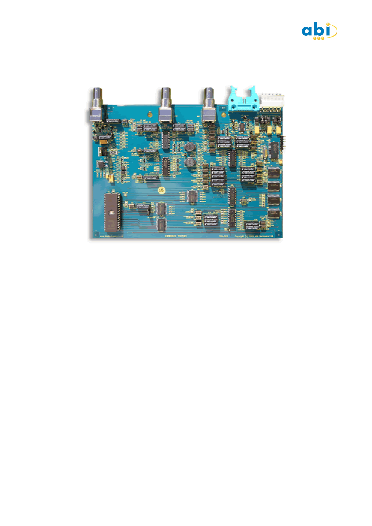
The board is divided into three distinct sections. A digital section with various digital ICs
including a microprocessor, memory and EPROM) is included to demonstrate the capabilities
of our IC Test Solution instruments. An analogue section contains analogue components to
demonstrate the functions of our Analogue V-I and Analogue IC Test Solutions. Finally, a
discrete section contains uncommitted discrete components to allow a more detailed analysis
of V-I and analogue testing. Products that combine different test techniques, such as the
Diagnostic Solution and the BoardMaster 8000 PLUS, can be used on the entire board.
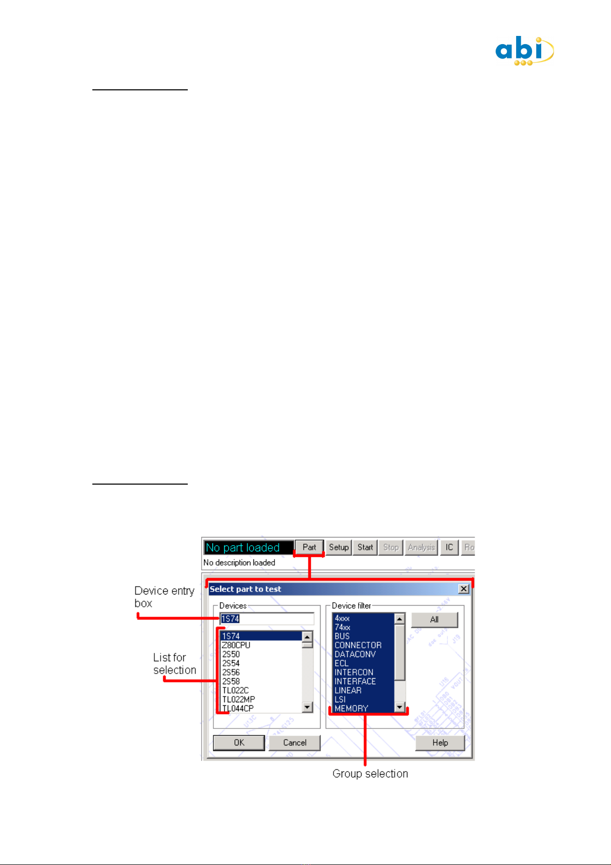
The board can be used in two ways. The relevant SYSTEM 8 instrument e.g. the IC Tester)
can be opened manually and configured to test a particular component on the training board.
The switches for the component can be used to simulate a fault condition, by reference to the
circuit diagram and/or this manual. The results can then be analysed to gain an
understanding of the operation of the system. Alternatively, the training board package
contains a CD-ROM with a test sequence file TestFlow), which can be used to guide the
operator through a sequence of tests on the board. All instruments are opened and
configured automatically, leaving the operator free to concentrate on analysing the results.
Brief instructions and explanations are also shown on screen. The disk also contains all
necessary data files e.g. digital pattern files, V-I data files etc.) which are required by some
of the test steps. We suggest that you work through this sequence file in order to gain a
thorough understanding of the system. You can also select individual steps in the sequence,
if you wish to repeat a test.
Using TestFlow
ACTION
On each step in the Test Instruction it will tell you what you need to do to carry out each test
step. Instructions will include component location, switch settings and instrument operations.
Most steps are independent of each other so you can jump to a specific test if you wish.
In normal operation click NEXT button to continue.
ESCRIPTION
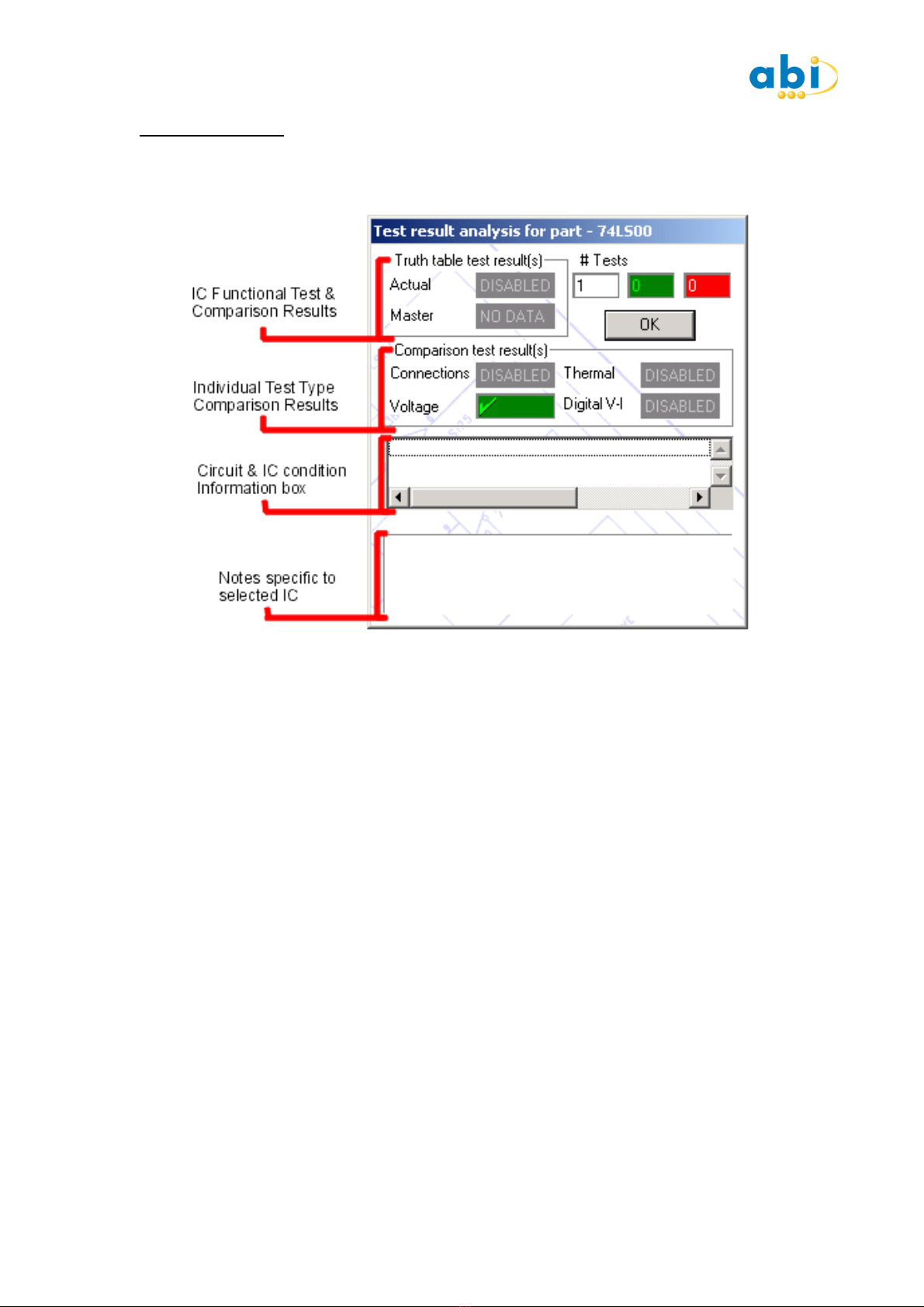
The Test Instruction describes the operation being carried out by the equipment and you.
Each step in the TestFlow is setup to allow information to be easily acccessed without
cluttering the screen. Each step in the TestFlow can show valid circuit and device conditions
and also fault conditions.
The TestFlow system) is originally intended to highlight fault conditions with a failure or bad
indication. For the purposes of training the TestFlow for the Training board will indicate a
pass or good comparison if the correct action has been carried out by the operator, indicating
that the particular point being covered in the TestFlow step has been correctly completed.
Page 3
Identifying Training PCB
ACTION
Identify the training board, as pictured below.
ESRIPTION
The purpose of the Training Board is to demonstrate all the functions of BOARDMASTER or
SYSTEM 8 modules. By providing examples of circuit and fault conditions the techniques of
fault with the equipment will be highlighted. The PCB includes simple circuits for training in
basic electronic principles.
The PCB is designed in sections to give optimum coverage for each aspect of the equipment.
Circuit and fault conditions are applied by making a switch connected to a PIC which in turn
energises relays that switch in components to alter the circuit.
Page 4
EXERCISE 1 : IGITAL IC TESTER
ACTION
Identify the sections of the IC Tester using description and Schematics.
ESCRIPTION
On first opening the IC Tester there is normally no part loaded from the device library.
Within the TestFlow the part is already loaded and cannot be changed by the user, this
reduces operator error and speeds up testing.
The PART button takes you to the device selection screen.
The SETUP button takes you to the test type, mode and comparison setup screen.
The START/STOP buttons execute and terminate the tests.
The ANALYSIS button opens the Analysis test results) window.
The IC button toggles between the IC diagram and V-I views after the test is completed.
The ACTUAL/MASTER toggles changes between views when comparing two test results.
The Arrow controls << < > >>) are used to step through individual pins or groups of pins
in the V-I curve view.
COMMENT
When running a TestFlow, control and setup is limited for the user, this is normally of great
benefit. For this instance it is advisable that familiarity with creating and using TestFlows is
done after you have completed the Training Board.
EXERCISE 2 : EVICE LIBRARY SELECTION
ACTION
View picture below and description to see the manual device selection methods.
Page 5
ESRIPTION
Device selection can be done in different ways. The simplest way is to type the number of the
device directly into the test box. The devices can be filtered down to specific groups to make
browsing easier. Multiple groups can be selected pressing the SHIFT key and then selecting
groups
COMMENT
For many devices there are prefixes and suffixes. In most cases it is not necessary to type in
these characters. If you identify the base number you can type in the first few characters and
then browse the device library offered in the list.
As with the 74xx series of devices where there are a range of different types, LS, AC,HC, AS
etc. It is important that you select a device with corresponding thresholds for the device
under test DUT). For example the threshold for and AC device is as a CMOS device threshold
so you must use the correct type to test the device properly. TTL has a high threshold of 2.4V
but the 74C type has a High threshold of 4.0V.
EXERCISE 3 : BOAR FAULT LOCATOR POWER SUPPLY
ACTION
Attach the red and black power lead from the training board connector to the BFL Supply.
ESCRIPTION
The BFL provides a 5V @5A supply for the IC tests. The entire PCB is powered by this supply
which is switched on and off as required by the tests you are running. Because a combination
of power-on and power-off can be run together it is the ideal supply to use as no errors of
running power-off tests with voltages present will occur. In the SETUP there is a delay option
that delays the time from the supply being switched on the test starting.
Page 6
COMMENTS
If you require a higher current for the UUT you can use an external supply for testing. It is
important that the external supply isreferenced to the BFL ground so that its measurements
are accurate. By not doing this it might be that the BFL will detect High Voltages and not start
the test.
EXERCISE 4 : VOLTAGE TEST
ACTION
Connect 64-way split cable to the Board Fault Locator Module If using a BoardMaster the
bottom module is the Primary test module).
Attach a 14,16 or 20 way DIL test clip to the black connectors on the 64 way cable with the
red stripe. Ensuring the clip is placed on the inner rows and towards the red stripe. Cable is
labelled accordingly.) Attach clip to IC U5 with red stripe orientated toward the pin 1 end of
IC see below) :
Press the SETUP button and take note of the Type and Mode settings as well as the
Thresholds. Close the SETUP window.
Press the START button and observe the IC diagram dragging the test results display to one
side if necessary.
ESCRIPTION
The Voltage test quite simply looks at the voltage on each pin in turn and displays the result.
Much like measuring each IC pin with a Multimeter but much quicker. When the voltage test
is selected on its own the clip is not automatically orientated due to the passive nature of the
test.
Clipping Pin 1 of the tester to Pin 1 of the IC makes it easy to identify which reading
corresponds to IC pin. When used independently each pin has an indication of the logic level
the voltage corresponds to. The logic level thresholds can be seen in the SETUP window and
the default settings are those for the device you have selected to test.
COMMENTS
It is advisable to run the voltage test in a Loop mode so that you can see if the DUT is active.
Changing logic states could indicate active signals on the PCB and device which may have to
be given special consideration when reviewing the later tests.
Page 7
EXERCISE 5 : TEST RESULTS ANALYSIS
ACTION
Press START on the IC Tester and observe the Test Results Analysis window.
ESCRIPTION
The Test Results Analysis window contains three sections, each giving different information.
1. The Truth Table Test Result gives a pass or fail result green or red) when a Truth Table
test has been carried out. If there is no Truth table selected No Data will be displayed. In this
section there is also a result box for the saved or Master result if the test is carried out from a
TestFlow or Live Comparison.
2. Comparison results section indicates whether the Connections, Voltage, Thermal and V-I
results were the same as those for the saved device within the TestFlow.
3. The Status window gives comment on the conditions the system finds present on the
device and advises on requirement of Ground Clip.
COMMENT
In normal one-off testing there will only be the actual Truth Table test result showing any
detail. With Live Comparison and TestFlow routines only the tests selected will apply a
comparison. All unselected tests will show No Data. Test that the system was unable to
perform such as tests resulting in a NoVcc or No Gnd indication will also show No Data.
Page 8
EXERCISE 6 : CONNECTIONS TEST
ACTION
Ensure clip securely on U5.
Go to SETUP and observe settings for Test Type and Mode. Close SETUP.
Press START on the IC Tester.
Observe results and conditions presented around device.
ESCRIPTION
The connections test forms an important part of the IC Tester. Every IC presents different
conditions on its pins. The connections test looks for these conditions to enable the Truth
Table test to be correctly applied. Connections can be related to the logic level seen on the
pins, whether the device has pins shorted to 5V or 0V, Open Circuit or Floating, Linked or
normally driven. The details of how the checks are carried out are included in the
presentation, "ABI Test Methodology", included on the CD.
COMMENT
The connections test on its own may not always highlight the fault but it is an integral part of
the ABI test philosophy, without it you will not be able to effectively diagnose a PCB. With a
truth table test the integrity of the IC is tested, to test it the system needs to obtain the
circuit connections to the IC, these Connections in turn can be used to compare against the
connections of a good IC or against the schematic of the PCB. In some cases the Connections
results are just as important as the Truth Table test as the connections information could
show a problem in the circuit even though the IC test passes the chip you are clipped on.
EXERCISE 7 : VCC ETECTION
ACTION
Press START on the IC Tester and observe indication in Red on Vcc pin pin 14) and voltage
reading. Press the NO VCC SWITCH and ensure LED lights is on. Observe the V+ indicator on
Pin 14 is now removed and NOV+ indication is now in its place.
Note there are no voltage readings.
Page 9
ESCRIPTION
Operating the NO VCC switch alters the circuit so that there is no supply voltage. This puts
the supply voltage below the threshold allowed by the BFL. This is the reason why the VCC
pin indicates NOV+. To ensure the correct operation of the Training board a good comparison
is achieved when the condition being covered is applied. For this reason the red flag
indicates the pin where there is a difference when compared with the MASTER Saved)
information.
COMMENTS
The threshold used by the BFL is 4.7V. When the connections test indicates NOV+ it could
either be No V+ present or V+ below allowed threshold. Both conditions should be
investigated further initially by switching off Connections test and using Voltage test in Loop
mode to verify the actual voltage present.
EXERCISE 8 : GROUN ETECTION
ACTION
Press START on IC Tester and observe GND indication on Pin 7.
Press NO GND switch and ensure LED lights.
ESCRIPTION
Operating the No GND switch alters the circuit so that the device Ground pin does not
present a valid ground to the tester.
COMMENT
In cases like this the first steps are to ensure the clip is connected/attached properly and
that the BFL supply is correctly referenced. If problem remains you must check the continuity
of the ground plane from the point of supply to the IC being tested. It may be that the PCB
has more than one Ground plane due to analogue and digital sections on the PCB.
EXERCISE 9 : AUTO CLIP POSITIONING
ACTION
Remove the clip from U5 and re-clip with opposite orientation. red stripe to bottom of IC).
Press START on the IC Tester and observe results on IC diagram.
ESCRIPTION
This step shows the systems ability to automatically orientate the channels to match the
position of the clip on the IC. As long as all the pins on the IC are covered by the clip and the
connection to Vcc and GND is good the auto-clip function will operate.
The IC Diagram will remain in the same orientation.
Page 10
COMMENT
The clip positioning function is very useful when devices are close together and when you
have many different size IC's to test. You can put one 20 way clip in the cable and use it on
all IC's up to this size any way around. Even if another supply or ground pin is straddled it will
still correctly orientate the device.
EXERCISE 10 : NO PIN CONNECTION INFORMATION
ACTION
Press STARTon the IC Tester. Observe that most of the pins on the IC have no connections
information showing.
ESCRIPTION
For pins that have no connections information it means that there was a valid logic level seen
on the pins.
COMMENTS
For carrying out the truth table tests it is important to remember that these pins can be
driven high and low by the tester as they are in a normal stable state.
EXERCISE 11 : TRUTH TABLE TEST
ACTION
Press SETUP and note the test types and modes selected. Close the window.
Press START on the IC Tester and observe the analysis window for the test results.
ESCRIPTION
The test Setup indicates that the Truth table test and Connections tests will be carried out.
The Truth Table will check the integrity of the IC giving a functional PASS/ FAIL result. The
circuit conditions will be taken into account prior to the test and the expected truth table
result will be modified accordingly.The test will be carried out in LOOP mode as this is the
best way to show the changing activity around the IC during testing. You will see from the
results that the IC's Truth Table result is a PASS given by the ACTUAL result in the Analysis
box. It is compared to the stored result of the MASTER or good IC test. This shows a good
comparison.
COMMENTS
The Truth Table test verifies the operation of the IC for how it sees it to be wired. It uses
the Connections information to automatically compensate for the circuit conditions giving you
a valid result each individual test in the Loop.
AUTOMATIC CIRCUIT COMPENSATION is a very important part of the IC tester. Its
usefulness can be seen in the next section of TestFLow steps.
Through backdriving, the tester effectively isolates the IC being tested from the influences of
surrounding components. It is important that the PCB be as stable as possible when testing
to reduce the effect of interference from external sources to the DUT. Please view
presentation titled, "ABI Test Methodology" and "Backdriving: The force behind the functional
test" for more detailed information on testing IC's.
Page 11
EXERCISE 12 : FLOATING PINS / RIVEN PINS
ACTION
Press START on IC Tester. Observe 'FLOT IPML' on pin 10.
Press INPUT DRIVEN switch to apply drive to Pin 10 from output on pin 11.
Observe FLOT signal change to L1 and also an L1 appearing on pin 11.
ESCRIPTION
In this step the circuit shows that there is a connection to input pin 10 but it is not being
driven as the relay is not being energised. Although there is no drive to the input it is not
registering as an open circuit due to the level of impedance measured.
Operating the 'INPUT DRIVEN' switch connects the output from Pin 11 to the input of Pin 10
via the relay. This shows how pins that are directly linked together are identified. The FLOT
indication is removed as the pin now has a valid logic level driven to it.
COMMENT
Floating pins are a common occurrence on TTL type devices. Whenever there is a Floating pin
identified there is likely be an indication of a MID LEVEL voltage. As the pin is not being
driven by a valid logic level and is floating between, there will be an indication of a Mid-High
or a Mid -Low voltage.
It is most important that you understand that this condition will be normal if the device has
a floating pin due to its lack of connection to another device. For instance, if the input comes
from a connector normally used in the system there may be an open circuit or a floating pin
displayed depending on the device it normally drives. It is not immediately recognised as a
fault condition, in most cases it would be a circuit condition.
Referencing against a good board or the schematics or even following the track to its source
can quickly verify the situation.
EXERCISE 13 : LINKE PINS
ACTION
Press START on the IC Tester.
Press the INPUT DRIVEN switch and verify Pins 10 & 11 each show L1.
Press the VALID LINK switch. Pins 1 & 2 now show L1 and pins 10 & 11 show L2.
Page 12
ESCRIPTION
The Connections test finds Links by changing the input state of one pin and monitoring all
subsequent pins for the same change. Pins found to be linked in this manner are then
checked by reversing the order of test. There is no limit to how many pins can be shown as
linked but there is differentiation between the groups as can be seen by two pins with L1
one linked pair) and L2 a separate linked pair not linked to L1).
COMMENTS
There is no significance in the numbering of pairs or groups of pins. The order is governed
by the Links seen first by the Connections test. A sign of activity on a PCB may be that the
links are constantly changing and moving about.
This would indicate a fast moving signal but it would also depend on the device operation for
instance a flip-flip with a high speed clock could give some confusing results with mid-levels
and linked pins if you were not aware of how the test results are obtained.
EXERCISE 14 : MI LEVEL INPUTS
ACTION
Press START on the IC Tester.
Press INPUT MID HIGH switch and observe the input on Pin 12 change to IPMH.
Press INPUT MID LOW switch and observe the input on Pin 13 change to IPML
ESCRIPTION
Supplying the input through a potential divider creates both of the conditions. Note from the
circuit that external components as well as fault conditions can create Mid-Levels.
COMMENT
Input Mid-Low and Input Mid-High can be present for a large number of reasons not
necessarily due to a fault condition. Circuit design and circuit conditions generally do present
mid-levels.
A fast changing signal will show a mid-level result, some open collector configurations will
show mid-levels due to pull-up resistor values. Each occurrence of mid-level input should be
considered along with what you know of the circuit and what other IC's in the circuit
show.Mid Level inputs generally do not give reason for a Truth Table test to fail. As long as
the tester can backdrive the signal the response from the IC should remain good. If the Mid-
level cannot be driven to a valid logic level then it will be identified as a problem.
EXERCISE 15 : INPUT SHORTS
ACTION
Press START on the IC Tester. Observe Truth Table test is PASS. Press SHORT 5V switch.
Observe change to Pin 4 and note the Truth Table test continues to PASS. Press SHORT 0V
button. Observe change to Pin 9 and note the Truth Table test continues to PASS.
Note the change to Pin 10 from FLOT to OPCT.
Page 13
ESCRIPTION
The shorted pins are directly connected to VCC & GND. The tester cannot drive these pins
and they remain in the same state throughout the test. Stimulus is not applied to the pins
and the Truth Table test is adjusted accordingly.
The OPCT indication on Pin 9 would, in normal circumstances indicate a pin not being driven
and not presenting any impedance.For CMOS it could be normal condition from high
impedance inputs, it could be a broken bond wire in IC, Tri-state output in OFF state or even
a bad clip connection.
In this case it represents the normal behaviour of a TTL gate with multiple inputs. When one
input is Floating and the other input is pulled LOW or to GND the internal diode structure of
the gate presents a high impedance to the tester on the floating pin. This is a typical feature
on TTL devices.
COMMENT
The Shorts presented to the inputs are taken into account as valid circuit conditions when the
Truth Table test is run. This test shows the ability of the system to adapt to different circuit
conditions and still give valid results for the IC Test without any operator intervention. In this
instance the end result tells you that the device is operating correctly for how it is wired,
whether the circuit conditions seen are valid would need the Connections tests to be run in
comparison with the results of a good board or checked against the schematic
EXERCISE 16 : INPUT LOA S
ACTION
Press START on the IC Tester.
Press INPUT LOAD 0V switch and observe change to Pin 5.
Press INPUT LOAD 5V switch and observe Pin 13
Note the Truth Table continues to show PASS.
Page 14
ESCRIPTION
The Load 0V is caused by the input pin being connected to VCC with a low resistance to
Ground 3.5Ohm) The drive channel of the system attempts to pull the pin to a high logic
level >2.4V for this device) but cannot obtain a valid logic High and so indicates that it is
loaded to 0V.
The system will try to drive the pin high for each successive loop. The Truth Table test will
be applied taking into account that the pin will remain in a Low state.
The Load 5V is a similar case where the tester attempts to take the pin to a Logic Low <0.5V
for this device). If it cannot drive the pin to a valid state it will indicate the LOAD and amend
the following Truth Table test.
COMMENT
Loads can be caused by high current devices driving the inputs of the DUT. Large capacitors
used in timing circuits could also give a load as they cannot change quickly enough when the
tester drives a voltage across it. Because they are input loads the tester will adapt the truth
table test to take the condition into account.
There is no operator intervention required other than to confirm the presence of the load is
acceptable due to the circuit design and components used. It is possible that an internal IC
static protection diode can give a LOAD indication.
EXERCISE 17 : OUTPUT MI LEVELS
ACTION
Press START on IC Tester. Operate MID HIGH FAULT switch and observe indication on Pin 6.
NOTE: Test Fails. Operate MID LOW FAULT switch and observe indication.
STOP the test and read the description.
ESCRIPTION
The input threshold levels on IC Tester can be changed in the SETUP dialogue box.
For TTL logic, the default settings are as follows:LOW: 0.5V, SWITCHING: 1.2V, HIGH: 2.4V
When a functional test is executed, the outputs of the IC under test are interpreted by
comparing them with the preset threshold-voltages. They would normally be either HIGH
above the HIGH threshold) or LOW below the LOW threshold). When the output voltage
however is between the LOW threshold and the SWITCHING threshold, a MID LOW message
will appear indicating a fault. Similarly when the output voltage is between the SWITCHING
threshold and the HIGH threshold, a MID HIGH fault message will appear.
On the training board, the fault has been simulated by connecting the output of a NAND gate
through relays to GND and VCC via suitable resistors. When the relay is open, no MID LEVEL
fault will be seen but when the relay is closed the IC cannot drive the resistor to a valid logic
level. The voltage is between the SWITCHING threshold but not at the valid level, thus
displaying a MID HI or MID LO or both depending on the test result the system expected.
COMMENT
This type of fault could be seen on the output of an IC that is genuinely faulty. It can also be
seen if the output is driving an input of another gate or device that was applying a loading
effect to such an extent that the driving stage could not reach its normal output voltage.This
shows that a MID LEVEL fault shown on the output of one IC may in fact indicate a problem
elsewhere in the circuit, as in the example on the training board.
Page 15
EXERCISE 18 : OUTPUT MI LEVEL WITH LOGIC TRACE
ACTION
Go to SETUP and select the LOGIC TRACE then exit SETUP.
Press START on the IC Tester and note the LOGIC TRACE window.
Press the MID-LEVEL switches again and observe the changes to the monitored values on Pin
6 by clicking on the LOGIC TRACE display at the relevant step.
ESCRIPTION
The LOGIC TRACE is an ideal tool for examining the behaviour of an output. In this case, the
outputs of Pin 6 seems to be giving conflicting information.
Being Mid-High and Mid-Low at the same is not exactly what it means. The Result shows all
the conditions seen on the pin for the whole test. Examining the LOGIC TRACE shows that
for a particular part of the test the result was Mid-High when a High was expected.
At another part of the test the result was Mid-Low when a LOW was expected. Examining the
LOGIC TRACE in will highlight the exact nature of the results because the trace is derived
from the actual TRUTH TABLE applied to the IC.
COMMENT
This type of fault could be seen on the output of an IC that is genuinely faulty. It can also be
seen if the output is driving an input of another gate or device that was applying a loading
effect to such an extent that the driving stage could not reach its normal output voltage. This
shows that a MID LEVEL fault shown on the output of one IC may in fact indicate a problem
elsewhere in the circuit, as in the example on the training board.
EXERCISE 19 : OUTPUT SHORTS
ACTION
Press START on the IC Tester.
ONLY APPLY A SHORT FOR SHORT PERIODS OF TIME TO AVOID DAMAGE.
Press OUTPUT SHORT 0V switch and Observe device failure and indication on Pin 8. When
satisfied remove SH0V. Press OUTPUT SHORT 5V switch and observe device failure due to
OUTPUT SHORT 5V on Pin 3.
ESCRIPTION
The maximum resistance to GND that will indicate a SHORT 0V is approximately 1.5 Ohms. If
a pin of an IC has a resistance less than 1.5 Ohms to GND then the SHORT 0V message will
appear. If the pin is an input, this may be a valid circuit configuration that is recognised by
AUTOMATIC CIRCUIT COMPENSATION and allowed for in the test. If however an output is
shorted to ground, this is regarded as a fault and a FAIL result occurs.
TRI-STATE and OPEN-COLLECTOR outputs however can be shorted to ground in some
designs, therefore a FAIL may not be indicated in these situations although the short is still
shown on the display.
Page 16
COMMENTS
The indication of an output short is a very positive indicator of a problem. Tri-state or open-
collector circuit design can be checked easily against a known good board or, as in all cases,
the circuit can be investigated further by checking the components being driven by the output
and a choice being made to remove a component and test independently.
EXERCISE 20 : SIGNAL ETECTION
ACTION
Press START on the IC Tester.
Press CHANGING SIGNAL switch and observe SIG indication on Pin 5.
Note the status will not show pass due to the alternating nature of the signal
ESCRIPTION
If an IC is being functionally tested on a board that has a clock oscillator running, and the
clock or fast signal derived from the clock is present on one or more pins of that IC, then a
SIGNAL message may appear in yellow on those pins. This message is an indication that a
changing signal has been detected on that pin. The test may be affected in such a way that a
good IC could FAIL.
COMMENTS
Changing signals on the board under test are one of the biggest causes of spurious test
failures. Even if they do not cause a particular test to FAIL, they may cause different circuit
conditions that can cause problems when comparing results between different boards using
test sequence or IC Live Comparison modes especially if comparing voltages.
In this test there are spurious bad comparisons even thought the SIGNAL is correctly
identified. There are MIDHI and MIDLO indications because of the voltage varying whilst the
measurement is being carried out therefore the saved result has to be only one of the values.
Page 17
EXERCISE 21 : SIGNAL REMOVAL - BUS ISABLE OUTPUT
ACTION
Attach clip to U15 74LS161).
Identify and attach the Bus Disable Output BDO) cable as shown in Schematic. If
Schematics are not available identify the clock signal by using the MIS Oscilloscope). Press
START on the IC tester and observe the SIG Pin 2. Attach a BDO LOW Green) to TP84 DIS
CLK and observe change to signal.
Note the Truth Table test will fail, as this IC requires a ground clip please go to the next step.
ESCRIPTION
Signals do not always cause device failures, in cases where they causes intermittent bad
comparisons also, it is advised the attempts are made to Stop the signal from affecting the
test. The way of disabling the signal without physically removing the source of the signal
from the board e.g. a crystal or oscillator). can usually be achieved using the bus disable
output BDO) cable.
On the training board a clock is generated by a capacitor, a resistor and an inverter which is
then fed through two NAND gates. The clock can be disabled and the output can be made
permanently LOW by using a LOW BDO green) on the clock buffer IC. By attaching the BDO
Low to TP84 the clock input to the NAND gate is pulled Low so achieving a stable output to
the IC we are testing. This enables the correct logic level to be driven into the IC for the
Truth Table test.
COMMENTS
When using the BDO signals, you must ensure that the point at which you connect the BDO
signal is not directly connected to the IC under test, otherwise the system will be driving itself
and you will get a LOAD indication. Note that the BFL inputs are capable of detecting signals
of up to about 4MHz. Signals above this frequency may not be detected, and you should
always be aware of this if spurious or inconsistent results are obtained. Running tests in loop
mode may show up these undetected signals, especially if the results are inconsistent and
continually changing. INPUT MID LEVELS are also often caused by changing signals above
the detectable frequency.
Either the BDO Low Green), or BDO High Red) can be used depending on the circuit
requirements. Alternative means can be used such as a RESET switch or use of BDO on a
CPU RESET pin and device removal.
It is important to remember that the more information you save about a good board the
better the chances of finding the fault when comparing with abad board. In this case you
should save the good device with the SIGNAL present and then in a later step describe how
the SIGNAL should be removed or allow the Truth Table test to Pass. In this way a potential
problem is not removed from the board prior to testing.
Page 18
EXERCISE 22 : B O & GROUN CLIP (BACK RIVING
NOISE)
ACTION
Identify the Ground clip and attach to the test cable as shown in Schematic. Place clip on IC
U15 74161). Ensure that the BDO LOW is attached to TP84 DIS CLK.
Press START on the IC Tester. Observe the failures and then apply the Ground Clip to the
GND point near to the Ground pin of the IC TP93.
ESCRIPTION
This device has a clock signal running to it that gives output failures but also the Analysis box
suggests that a Ground Clip may be required. The Ground Clip is used to reduce backdriving
noise. This noise is caused by current surges when backdriving IC outputs. On the training
board we have used a 74S00 a relatively high current output IC) to drive a clock signal
into a 74LS161. As part of the 74LS161 test, the SYSTEM 8 pin drivers must output a clock
signal to the CLK pin pin 2) to test the functionality of the IC. In this situation, the existing
clock on the board under test is "backdriven" by the SYSTEM 8 pin driver. This process
requires larger than normal current of a magnitude that depends on the device being
backdriven. It is particularly large when driving a pin that is in the LOW state since the output
sink current of most logic families is higher than their source current. This large current can
cause "ground bounce" on the board, which may cause double clocking of a sequential device
such as a counter or shift register. If double clocking occurs, the test will FAIL because the
test program gets out of step with the operation of the IC under test.
To remove this noise, the ground clip must be used as it provides a shorter ground return
path back to the SYSTEM 8 pin driver. The ground clip should be placed as near as possible
to the GND pin of the IC under test.
Page 19
COMMENTS
When testing sequential ICs such as counters, shift registers or flip-flops, you should always
be aware of backdriving noise and the need to use the ground clip. The phenomena is
however highly dependent on many factors outside your control, amongst them temperature,
supply voltage, threshold voltage tolerances, output current tolerances and local ground
conditions. The above test is very difficult to reproduce in varying conditions, and you may
well find that the test passes without the ground clip, or fails even with the ground clip
connected. It may also PASS and FAIL intermittently. This is not typical of most boards you
will come across but you must be aware of the possibility of it occurring.
Note that the SYSTEM 8 software is aware of the ICs that may require the ground clip and a
warning is given in the analysis box after the test.
EXERCISE 23 : INVALI LINKS
ACTION
Clip on U15 74LS161. Ensure Ground Clip is attached to TP95 GND and BDO LOW is attached
to TP84 DIS CLK. Press STARTon the IC tester. Press INVALID LINK and COUNTER RELOAD.
Observe Failure indicators in both cases.
ESCRIPTION
Invalid LINKS can be caused by solder shorts, PCB faults or internal IC faults and can be in
many configurations on numerous ICs. They may also be caused by novel or unexpected
ways of using an IC in a design, which the AUTOMATIC CIRCUIT COMPENSATION software is
incapable of resolving. They are difficult to identify as Links but the indication is valid when
the circumstances are understood. The tester informs you of what is seen when testing the
device. It has flagged a failure for the device and you must investigate the problem to find
the root cause.
Page 20
COMMENTS
Invalid LINKS can be caused by solder shorts, PCB faults or internal IC faults and can be in
many configurations on numerous ICs. They may also be caused by novel or unexpected
ways of using an IC in a design, which the AUTOMATIC CIRCUIT COMPENSATION software is
incapable of resolving. They are difficult to identify as Links but the indication is valid when
the circumstances are understood. The tester informs you of what is seen when testing the
device. It has flagged a failure for the device and you must investigate the problem to find
the root cause.
EXERCISE 24 : TRI-STATE EVICES
ACTION
Ensure BDO is removed. Attach SOIC Test Cable the BFL. Attach 20 way or more SOIC clip to
cable. Attach clip to U13 74LS244 and press STARTon the IC tester. Observe test result.
ESCRIPTION
In many designs, the TRI-STATE outputs of one IC will be connected to the outputs of
another IC in a bus-structured configuration. In normal operation, the logic on the board will
ensure that only one output at a time can be enabled. From studying the circuit you can see
that the tester can backdrive the Enable signal Pins 1 & 19) to carry out a complete and
effective test on this device as the Address lines on the other device on the bus U10) are not
enabled so there will be no output contention.
COMMENTS
The Preliminary and connections tests carried out by the tester identify if there will be a
problem from other devices on the same bus. By 'Disabling' the device under test the tester
will then monitor all the outputs for a logic condition. As the device is turned off, the outputs
should all be Open Circuit high Impedance).
Note to illustrate this further the BDO green) can be connected to TP1 to disable the IC. The
outputs are then Open Circuit.
If it is seen that there is activity on the outputs then the device will show CONFLICTS.
Conflicts do not necessarily mean a device failure. This is due to the coincidence of the logic
levels such that there will be no failure of an output if there is a Logic High present from
another device on the bus at the same time as an expected Logic High output from the
device under test.

Other abi Test Equipment manuals

abi Professional ChipMaster Compact User manual

abi

abi Professional ChipMaster Compact User manual

Popular Test Equipment manuals by other brands

Rion NC-74 instruction manual

Rion

Rion NC-74 instruction manual

PIE 530 operating instructions

PIE

PIE 530 operating instructions

Gossen MetraWatt SECULIFE ST PRO manual

Gossen MetraWatt

Gossen MetraWatt SECULIFE ST PRO manual

Cirris 4200 Series quick start guide

Cirris

Cirris 4200 Series quick start guide

Hantek IDSO quick guide

Hantek

Hantek IDSO quick guide

Tamson Instruments TV12 user manual

Tamson Instruments

Tamson Instruments TV12 user manual

Viavi SmartOTDR Quick Card

Viavi

Viavi SmartOTDR Quick Card

Honeywell Vibrex 2000 user guide

Honeywell

Honeywell Vibrex 2000 user guide

Huazheng HZDL-2000III manual

Huazheng

Huazheng HZDL-2000III manual

Testboy Testavit Schuki 3 LCD operating instructions

Testboy

Testboy Testavit Schuki 3 LCD operating instructions

Neware CE-6000n user manual

Neware

Neware CE-6000n user manual

GW Instek PEL-3000 Series quick start guide

GW Instek

GW Instek PEL-3000 Series quick start guide

UGO BASILE 47883 instruction manual

UGO BASILE

UGO BASILE 47883 instruction manual

Zhurui-tec LPT100 user manual

Zhurui-tec

Zhurui-tec LPT100 user manual

SKF TKST 21 Instructions for use

SKF

SKF TKST 21 Instructions for use

Hurco Power Smoker 2 Reference manual and user's guige

Hurco

Hurco Power Smoker 2 Reference manual and user's guige

Tescom MTP200B operating manual

Tescom

Tescom MTP200B operating manual

Daekyung DTR-300N Operation manual

Daekyung

Daekyung DTR-300N Operation manual

manuals.online logo
manuals.online logoBrands
  • About & Mission
  • Contact us
  • Privacy Policy
  • Terms and Conditions

Copyright 2025 Manuals.Online. All Rights Reserved.