CAES GR-VPX-XCKU060 User manual

© Cobham Gaisler AB
Kungsgatan 12 | SE-411 19 Goteborg | Sweden
+46 31 7758650 | www.caes.com/gaisler
GR-VPX-XCKU060 Carrier Board
GR-VPX-XCKU060
GR-VPX-XCKU060-DSUM
Mar 2022, Version 1.1
Features
•Xilinx XCKU060, in 1517 pin FCBGA package
•GR716B (initially with GR716A)
microcontroller
•SODIMM DDR3 up to 8 GiB
•SPI flash for FPGA configuration (512 Mbit),
for GR716 boot (256 Mbit), and for data
(256 Mbit)
•Power, Reset, Clock and Auxiliary circuits
•Three FMC Mezzanine expansion connectors
•Scrubbing interface for FPGA
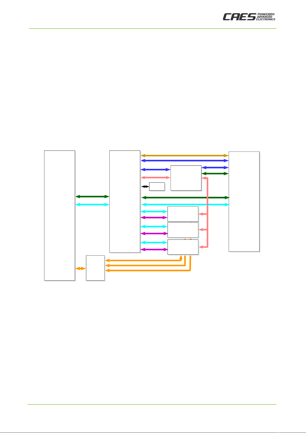
•Backplane I/F: SpaceWire (control),
SpaceFibre (data), VPX utility management
•Frontplane I/F and drivers: 4x SpaceFibre,
2x SpaceWire, USB/FTDI UART/JTAG Links,
USB I/F to FMC
•OpenVPX compatible, 6U format, Payload
profile
Description
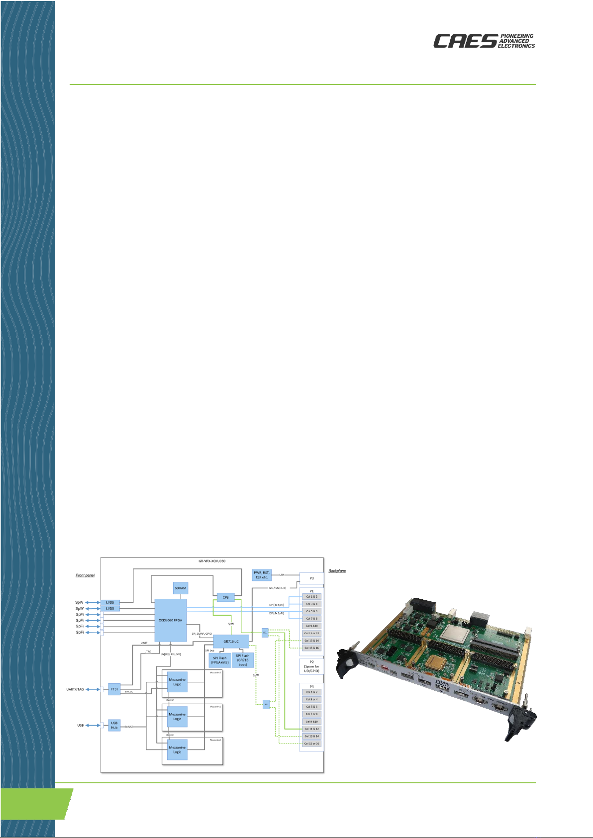
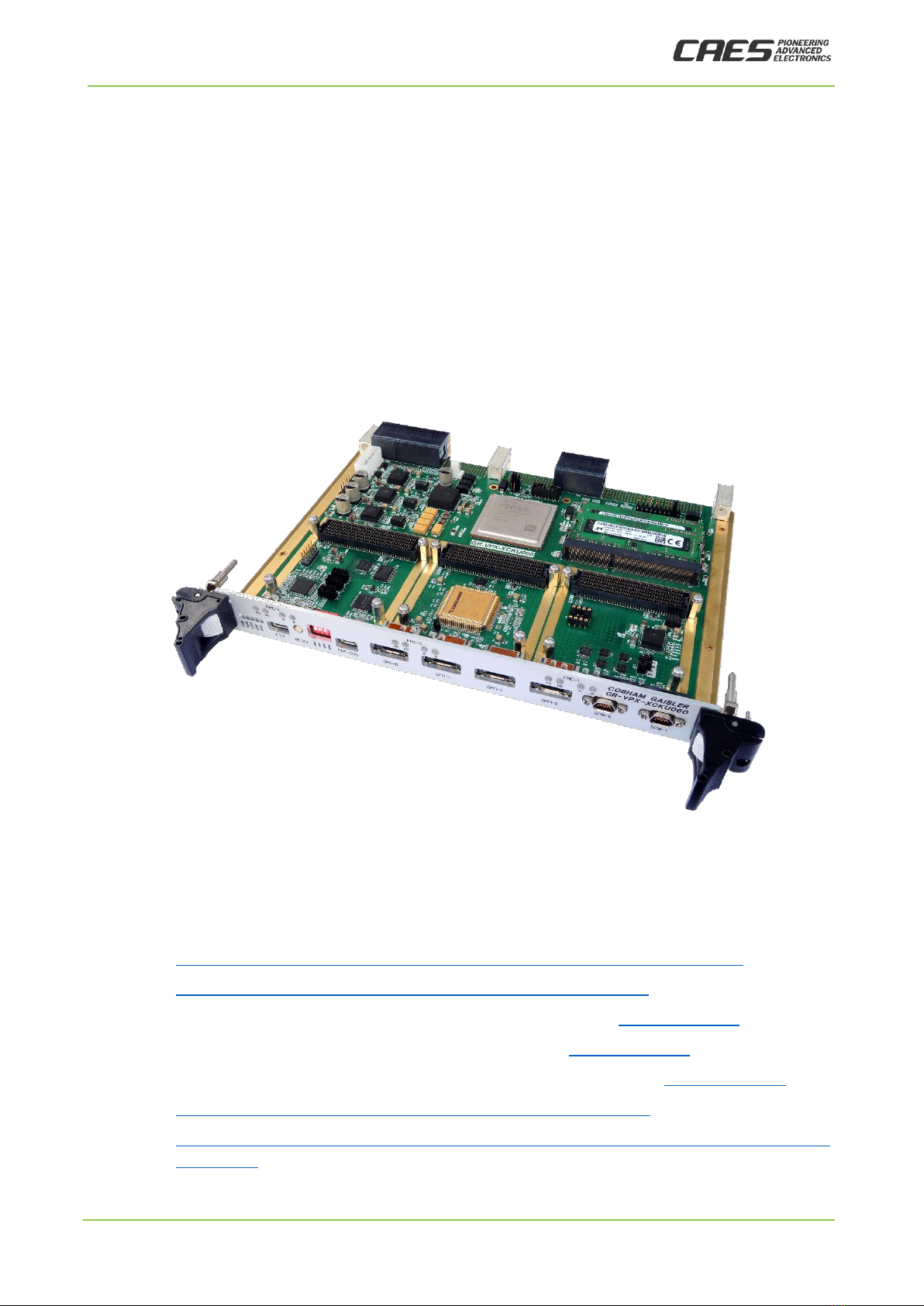
The GR-VPX-XCKU060 board features a Xilinx
Kintex Ultrascale XCKU060 FPGA and a
GR716 microcontroller acting as a supervisor
for the FPGA. The board is equipped with
three VITA 57.1 FMC connectors. It can be
operated without any Mezzanine board but is
specifically designed to be used with 1 to 3
GR-HPCB-FMC-M2 Mezzanine Boards
connected, each with a Myriad™ 2 M2450
Processor. The GR-HPCB-FMC-M2 boards are
not included with the GR-VPX-XCKU060
board.
Specifications
•System frequency GR716 uC: 20MHz, FPGA
XCKU060: 50 MHz
•5 x SpaceFibre links rated @ 3.125 Gbps
and 2 x SpaceWire links @ 200 Mbps
•CIF and LCD data interfaces 16-bit
running at 150 MHz. 24-bit interface
tested allowing upper bound 1.44Gb/s
full-duplex data transfer
•Typical power consumption <10W (excluding
mezzanines)
•DC supply via OpenVPX backplane connector
or via +5V/12V DC header for stand-alone
use
Applications
The board is a commercial development board for
prototyping of high-performance application such as:
•Earth Observation optical and radar payload
processing
•Multi- and hyperspectral data compression
•Visual-Based Navigation acceleration
•Video processing
•AI/ML processing, such as:
oImage segmentation (e.g. cloud
screening and removal)
oObject detection (e.g. fire detection)
oPose estimation
The applications can be allocated to the on-board
FPGA or shared with technology implemented in up
to three Mezzanine boards, configured either for
increased performance or for redundancy
applications. The control and supervision of the
FPGA and Mezzanine boards is handled by a rad-
hard microcontroller.
Data Sheet & User Manual

© Cobham Gaisler AB
Kungsgatan 12 | SE-411 19 Goteborg | Sweden
+46 31 7758650 | www.caes.com/gaisler
2
GR-VPX-XCKU060
GR-VPX-XCKU060-DSUM
Mar 2022, Version 1.1
TABLE OF CONTENTS
1Introduction..................................................................................................................................4
1.1 Scope of the Document .........................................................................................................4
1.2 Reference Documents............................................................................................................4
1.3 Document Revision Information...........................................................................................5
1.4 Abbreviations ........................................................................................................................5
2Architecture..................................................................................................................................6
3Configuration and Installation .....................................................................................................7
3.1 Electrical installation.............................................................................................................7
3.2 Notes on VITA 57.1 compliance ...........................................................................................7
4Functional Blocks ........................................................................................................................8
4.1 Memory .................................................................................................................................8
4.2 Xilinx Kintex Ultrascale FPGA ............................................................................................8
4.3 GR716 microcontroller..........................................................................................................9
4.4 Oscillators and Clock Inputs .................................................................................................9
4.5 Reset Circuits ......................................................................................................................10
4.6 Power Supply and Voltage Regulation................................................................................11
4.6.1 Overview......................................................................................................................11
4.6.2 Power sequencing ........................................................................................................12
4.6.3 FMC Power Supplies ...................................................................................................14
5Interfaces....................................................................................................................................15
5.1 Overview .............................................................................................................................15
5.2 Front panel interfaces ..........................................................................................................16
5.3 Backplane interfaces............................................................................................................17
5.4 On-board interfaces .............................................................................................................17
5.5 SpFi .....................................................................................................................................18
5.6 SpW Interfaces ....................................................................................................................20
5.7 SPI .......................................................................................................................................22
5.8 I2C.......................................................................................................................................24
5.9 FTDI (USB Serial/Jtag).......................................................................................................25
5.10 JTAG ...................................................................................................................................25
5.11 USB .....................................................................................................................................26
5.12 FMC Interfaces....................................................................................................................26
5.12.1 Overview......................................................................................................................26
5.12.2 FMC Interface Summary .............................................................................................26
5.12.3 LCD..............................................................................................................................29

© Cobham Gaisler AB
Kungsgatan 12 | SE-411 19 Goteborg | Sweden
+46 31 7758650 | www.caes.com/gaisler
3
GR-VPX-XCKU060
GR-VPX-XCKU060-DSUM
Mar 2022, Version 1.1
5.12.4 CIF ...............................................................................................................................30
5.12.5 SPI0..............................................................................................................................30
5.12.6 SPI1..............................................................................................................................30
5.12.7 SPI2..............................................................................................................................30
5.12.8 USB..............................................................................................................................30
5.12.9 JTAG ............................................................................................................................31
5.12.10 SYS-RSTN...................................................................................................................31
5.12.11 WAKEUP .....................................................................................................................32
5.12.12 HEARTBEAT[1..0]......................................................................................................32
5.12.13 GA[1..0] .......................................................................................................................32
5.12.14 +12V ............................................................................................................................32
5.12.15 ENABLEN...................................................................................................................32
5.12.16 PWR-GOOD ................................................................................................................32
5.12.17 S[3..0]...........................................................................................................................32
5.12.18 I2C................................................................................................................................33
5.13 VPX Backplane Interface....................................................................................................33
5.14 Power...................................................................................................................................40
5.15 Headers................................................................................................................................40
5.15.1 J11 – FPGA JTAG........................................................................................................40
5.15.2 J12 - Power...................................................................................................................40
5.15.3 J13 - Optional SM-bus .................................................................................................41
5.15.4 J14 - Optional FPGA fan..............................................................................................41
5.15.5 J15 - Optional PM bus .................................................................................................41
5.16 Switches and buttons...........................................................................................................41
5.16.1 S2 - DIP Switch............................................................................................................41
5.16.2 JP1 - SelectMAP ..........................................................................................................42
5.16.3 JP2 - FPGA spare .........................................................................................................43
5.16.4 JP3 - SpW cross-point switch settings .........................................................................43
5.16.5 JP4-JP6 - UART and JTAG access ..............................................................................44
5.17 LEDs....................................................................................................................................44
5.17.1 D6 - FPGA initiation....................................................................................................44
5.17.2 D11 – VIN....................................................................................................................44
5.17.3 D12 - PG_C2M ............................................................................................................44
6Mechanical Description .............................................................................................................45

© Cobham Gaisler AB
Kungsgatan 12 | SE-411 19 Goteborg | Sweden
+46 31 7758650 | www.caes.com/gaisler
4
GR-VPX-XCKU060
GR-VPX-XCKU060-DSUM
Mar 2022, Version 1.1
1INTRODUCTION
1.1 Scope of the Document
This document describes the design for the GR-VPX-XCKU060 Development Board.
The main elements of this board are a Xilinx Kintex Ultrascale XCKU060 FPGA [RD1]
and a GR716 microcontroller [RD2].
This board is designed and intended to be used with the GR-HPCB-MEZZ-M2 Mezza-
nine Board but is conceived also to fulfil the requirements of standard VITA57.1 for FMC
Carrier boards [RD3].
Figure 1 GR-VPX-XCKU060 Carrier Board
1.2 Reference Documents
[RD1] https://www.xilinx.com/products/silicon-devices/fpga/kintex-ultrascale.html
[RD2] https://www.gaisler.com/index.php/products/components/gr716
[RD3] ANSI/VITA 57.1 FPGA Mezzanine Card (FMC) Standard, https://vita.com/
[RD4] ANSI/VITA 65.0-2017 OpenVPX System Standard, https://vita.com/
[RD5] DRAFT VITA 78.00-2015 rev 1.15 SpaceVPX System Standard, https://vita.com/
[RD6] https://www.ti.com/tool/FUSION-DIGITAL-POWER-STUDIO
[RD7] https://www.xilinx.com/support/documentation/user_guides/ug576-ultrascale-gth-trans-
ceivers.pdf
[RD8] Datasheet and User Manual for GR-HPCB-FMC-M2 Mezzanine Board, doc. no GR-

© Cobham Gaisler AB
Kungsgatan 12 | SE-411 19 Goteborg | Sweden
+46 31 7758650 | www.caes.com/gaisler
5
GR-VPX-XCKU060
GR-VPX-XCKU060-DSUM
Mar 2022, Version 1.1
HPCB-FMC-M2-DSUM
[RD9] https://www.xilinx.com/support/documentation/user_guides/ug575-ultrascale-pkg-
pinout.pdf
[RD10] GR-VPX-XCKU060 Board Package, see https://www.gaisler.com/index.php/prod-
ucts/boards/gr-vpx-xcku060
1.3 Document Revision Information
Version
Date
Section / Page
Description
1.0
2022-01-31
First approved issue.
1.1
2022-03-09
Page 1
Sec. 1.2
Editorial corrections of “Applications” and RD references.
1.4 Abbreviations
ASIC
Application Specific Integrated Circuit.
DCDC
DC DC Converter circuit
DDR
Double Data Rate
DSU
Debug Support Unit
ESA
European Space Agency
ESD
Electro-Static Discharge
ESTEC
European Space Research and Technology Centre
FP
Front Panel
FPGA
Field Programmable Gate Array
GPIO
General Purpose Input / Output
I/F
Interface
I/O
Input/Output
LDO
Low-Drop-out
MUX
Multiplexer
PB
Push-Button
PCB
Printed Circuit Board
RTC
Real Time Clock
SOC
System On a Chip
SPFI
Space Fibre
SPW
SpaceWire

© Cobham Gaisler AB
Kungsgatan 12 | SE-411 19 Goteborg | Sweden
+46 31 7758650 | www.caes.com/gaisler
6
GR-VPX-XCKU060
GR-VPX-XCKU060-DSUM
Mar 2022, Version 1.1
2ARCHITECTURE
This board is designed and intended to be used as an FPGA development board compris-
ing the following main elements:
•Front panel connectors and interfaces
•Xilinx Kintex Ultrascale FPGA plus power supplies and associated components
•GR716 microcontroller plus associated components
•Three FMC Mezzanine board connectors for expansion
•On Board DDR3 Memory
•VPX Backplane interface and connectors
Figure 2 GR-VPX-XCKU060 Development Board
Three FMC Mezzanine board sites are implemented on the carrier board.
These interfaces have been initially designed to each accommodate a GR-HPCB-FMC-
M2 Mezzanine board with and MA2450 processing components, and the FMC interfaces
are primarily assigned to accommodate this mezzanine board [RD8].
The pin definitions have been assigned to follow the assignment of the VITA57.1 speci-
fication [RD3] for FMC mezzanine boards to make the board suitable for use with other
FMC-compatible mezzanine boards. The board can also be used without any Mezzanine
boards.
It is designed to be used on a VITA 65 OpenVPX platform [RD4], specifically as a pay-
load module compatible with the slot profile SLT6-PAY-4F1Q2T-10.2.1.
The main components and functional blocks described in section 3.
GR716
MICRO-
CONTROLLER
GR716
MICRO-
CONTROLLER
VPX
BACKPLANE
VPX
BACKPLANE
SPW x 2 LINKS
SPW x 2 LINKS
SPACE FIBRE x 8 LINKS
CLOCKS
SPW x 2 LINKS
GPIO (TBD)
FRONT PANEL
FRONT PANEL FMC1
FMC1
SPI
GPIO (TBD)
SPACE FIBRE x 4
ULTRASCALE
KINTEX FPGA
XCKU060
ULTRASCALE
KINTEX FPGA
XCKU060
GPIO (TBD)
USB
USB
USB
4-WAY
USB HUB
4-WAY
USB HUB
USB
CTRL/DATA LINK
CTRL/DATA LINK
CTRL/DATA LINK FMC3
FMC3
FMC2
FMC2
SPACE FIBRE x 4
SPACE FIBRE x 4
SPACE FIBRE x 4
DDR3
DDR3

© Cobham Gaisler AB
Kungsgatan 12 | SE-411 19 Goteborg | Sweden
+46 31 7758650 | www.caes.com/gaisler
7
GR-VPX-XCKU060
GR-VPX-XCKU060-DSUM
Mar 2022, Version 1.1
The main interfaces of the board are described in section 5.
The mechanical format of the board is described in section 6.
3CONFIGURATION AND INSTALLATION
3.1 Electrical installation
The board is designed for installation in a payload slot profile variant SLT6-PAY-4F1Q2T-
10.2.1 as defined in the VITA 65 OpenVPX standard [RD4]. For operation, sufficient
current capabilities of the +5V and +12V supply lines provided by the VPX backplane is
to be confirmed, see below.
As an option, it can also be used in a stand-alone configuration, using the available head-
ers for supply and communication, see section 5. Connection details for supply is de-
scribed in sections 5.14 and 5.15.2. The connector allows for a dual supply with +5V and
+12V DC. For the Carrier Board itself, only +5V is required, with a capability of at least
3A is recommended. The +12V is only routed to the FMC mezzanine connector. Capabil-
ity required for the +5V and +12V leads depends on consumption of the Mezzanine
boards.
3.2 Notes on VITA 57.1 compliance
With some exceptions the GR-VXP-XCKU060 board is designed to comply with the rules
in the VITA 57.1 FMC standard [RD3]. Due to constraints on the Mezzanine board [RD8]
it was designed for there are some deviations to the rules and recommendations listed
below.
•VADJ is fixed to 1.8V and always enabled. Only mezzanines supporting 1.8V
operation can be used.
oRule 5.123, and related rules 5.9, 5.10, 5.122)
•Two of the HPC pins (J9/J10, FMC signals HA07_P/N) are connected to a 3.3V
bank (as I2C signals) while the other HAxy pins are connected to 1.8V banks.
Hence an HPCB mezzanine for 1.8V VADJ with pins connected to HA may be
subjected to overvoltage (3.3V).
oRule 5.1 (and to some extent related rules 5.3, 5.114)
•Rules about differential pairs are not fully implemented. For example, G6/G7
(LA00_P_CC/LA00_N_CC) do not connect to a differential pair on the FPGA.
This makes it impossible to use LVDS signalling on those pins.
oRecommendation 5.1
•The VREF mezzanine-to-carrier signals are not connected. This may degrade the
performance of signalling standards that require a reference voltage (such as
SSTL18 and HSTL18).
oRule 5.114 (and to some extent related rules 5.3, 5.4)
•Rules about clock capable pins are not fully implemented. Firstly LA00_CC_P/N,
LA01_CC_P/N, LA17_CC_P/N, and LA18_CC_P/N are not connected to FPGA
clock input capable pins. Secondly, although CLK0_M2C_P and CLK1_M2C_P
connect to clock capable FPGA pins, the complementary CLK0_M2C_N and
CLK1_M2C_N are disconnected. Hence LVDS clocks cannot be used for these

© Cobham Gaisler AB
Kungsgatan 12 | SE-411 19 Goteborg | Sweden
+46 31 7758650 | www.caes.com/gaisler
8
GR-VPX-XCKU060
GR-VPX-XCKU060-DSUM
Mar 2022, Version 1.1
pins.
oFor some pins: rules 5.24, recommendations 5.1, 5.5
•USB 2.0 signals are connected to LA33_P/N. These pins will be driven with 3.3V
despite VADJ being 1.8V.
oRule 5.123, and related rules 5.9, 5.10, 5.122)
Some of the deviations above are allowed, if information is provided to the user as above,
for example by the permissions below:
•Permission 5.10: If the signalling standard on Bank A does not require a reference
voltage, then the mezzanine module may leave VREF_A_M2C unconnected
•Permission 5.13: VADJ may be used for other purposes beyond its use for Bank
A IO supply voltage.
4FUNCTIONAL BLOCKS
4.1 Memory
Several types of memory are required for the various functions:
Table 1 Summary of on-board memory
SPI Flash for FPGA configuration
512Mbit
Cypress (Spansion) S25FL512S
DDR3 for FPGA working memory
Up to 8 GB
SODIMM 204 connector, 64bit inter-
face
SPI Flash for GR716 boot/data PROM
256Mbit
S25FL256L
SPI Flash for GR716 data PROM
256Mbit
S25FL256L
4.2 Xilinx Kintex Ultrascale FPGA
The board design incorporates a Xilinx XCKU060 FPGA in a FFVA1517C package.
This device has a footprint of 40 x 40mm.
The FPGA is a complex device requiring many high current and well-regulated power
supplies.
The assignment signals and the VCC_IO must take account of assignment and compati-
bility rules, and allow a logical ‘flow’ of signals according to the geometrical placement
of the components on the board.
The I/O Bank assignment is represented in Figure 3 below.
Notes:
•In Kintex Ultrascale, HP banks must operate at a VCC_IO voltage of 1.8V or
lower.
•The HR banks (Banks 64 & 65 on XCKU060-FFVA1517) may be operated at
2.5V or 3.3V.
•LVDS signals should operate with a bank voltage of 1.8V for best compatibil-
ity with the internal LVDS termination capabilities.
•The DDR3 interface must operate with an I/O voltage of 1.5V.

© Cobham Gaisler AB
Kungsgatan 12 | SE-411 19 Goteborg | Sweden
+46 31 7758650 | www.caes.com/gaisler
9
GR-VPX-XCKU060
GR-VPX-XCKU060-DSUM
Mar 2022, Version 1.1
Figure 3 FPGA Bank Assignment
4.3 GR716 microcontroller
The GPIO pins are configured to allow the following interfaces of the GR716 to be used:
•SPIM (for Boot program load from SPI memory)
•SPIM1 (for data load from SPI memory)
•DSU UART connection to FTDI USB circuit
•Application UART connection to FTDI USB circuit
•Redundant CMOS SPW1 pins connected to backplane via LVDS transceivers
•LVDS interface configured as SPW0
•I2C slave connection to SMBUS pins on VPX backplane
•I2C master connection for control/data connection to FMC circuits
•SPIO0 as master for control/data connection to FPGA
•SPIO1 as master for control/data connection to FMC circuits
•22 x GPIO connected to FPGA for signalling purposes
4.4 Oscillators and Clock Inputs
The oscillator and clock scheme for the GR-VPX-XCKU060 Board is shown in Figure 4
below.

© Cobham Gaisler AB
Kungsgatan 12 | SE-411 19 Goteborg | Sweden
+46 31 7758650 | www.caes.com/gaisler
10
GR-VPX-XCKU060
GR-VPX-XCKU060-DSUM
Mar 2022, Version 1.1
•The GR716 can optionally use a 20MHz crystal to generate its system clock. How-
ever it is not fitted by default since current GR716
• Instead, the GR716 main system clock input is a 20MHz, 3.3V oscillator.
•For flexibility in clocking, a separate 50MHz 3.3V oscillator is used for the
GR716 SPW_CLK input
•The FTDI UART circuit requires a dedicated 12MHz Crystal and generates its
own internal oscillator with this crystal.
• The FPGA is supplied with two clocks for general use. CLK1 is a 50 MHz/1.8V
oscillator soldered onto the board and CLK2 is a DIL 8 pin socket for a user de-
fined 3.3 V oscillator.
•A 300 MHz LVDS oscillator is dedicated to the DDR3 interface.
•A 156.25MHz LVDS oscillator is provided for the GTH clock. This clock is con-
nected to MGTREFCLK0, from which the other internal MGT clocks must be
derived.
•Two LVDS backplane clocks (REF_CLK, AUX_CLK) are connected directly
from backplane to the FPGA. The FPGA logic will have to determine how these
clocks are used (nominally these are input clocks to the FPGA).
Figure 4 Board level Clock Distribution Scheme – GR-VPX-XCKU060
4.5 Reset Circuits
The reset scheme for the GR-VPX-XCKU060 Board is shown in Figure 5 below.
The GR716 has its own internal reset circuitry.

© Cobham Gaisler AB
Kungsgatan 12 | SE-411 19 Goteborg | Sweden
+46 31 7758650 | www.caes.com/gaisler
11
GR-VPX-XCKU060
GR-VPX-XCKU060-DSUM
Mar 2022, Version 1.1
A TPS3705-33 reset supervisor provides a RSTN signal for the FPGA. The reset condi-
tions for controlling the RSTN signal are:
•Front panel push button switch
•Backplane (VPX) System Reset
•+12V power good (PFO/PFI functionality of TPS3705-33)
•+3V3 power good (internal functionality of TPS3705-33)
•Watchdog (RESET_OUT_N for GR716)
Figure 5 Board level Reset Scheme – GR-VPX-XCKU060
One I/O for each GR-HPCB-FMC_M2 mezzanine is a reset input controlled by the FPGA.
4.6 Power Supply and Voltage Regulation
4.6.1 Overview
The power supply system of the GR-VPX-XCKU060 board requires many voltages to be
generated and distributed, some of which have high current requirements (e.g. FPGA core
voltage).
Typically, the power requirements must be over-dimensioned since the actual current con-
sumption per rail is either unknown or varies depending on the application implemented
in the FPGA logic.
The power circuitry occupies a significant PCB area (about one fifth), even with highly
integrated commercial DC/DC modules are used.
A summary of the voltages required on the board is given in the table below.
Table 2 Summary of on-board voltages

© Cobham Gaisler AB
Kungsgatan 12 | SE-411 19 Goteborg | Sweden
+46 31 7758650 | www.caes.com/gaisler
12
GR-VPX-XCKU060
GR-VPX-XCKU060-DSUM
Mar 2022, Version 1.1
Device
Voltage
Dimensioning
Current
Function
VIN
12V
-
From backplane to FMC slots
VIN
5V
-
From backplane to DCDC inputs
XCKU060
3.3V
2A
VCC_IO, SPI prom
XCKU060
1.8V
<0.5A
VCCAUX, VCC_IO
XCKU060
1.5V
>3A
For DDR3 interface
XCKU060
0.95V
>10A
Vcore
XCKU060
GTH_1.8V
<0.5A
MGTVCCAUX
XCKU060
GTH_1.2V
1A
MGTREF, MGTAVTT
XCKU060
GTH_1.0V
1A
MGTAVCC
DDR3
1.5V
>5A
DDR3
0.75V
3A
DDR3 Termination voltage
GR716
3.3V
250mA
Assume single voltage mode using
internal GR716 regulator for 1.8V
FMC-1
12V
1A
FMC-2
12V
1A
FMC-3
12V
1A
Peripherals
3.3V
< 0.5A
Interface circuits
USB-HUB
1.1V
<0.3A
For USB Hub Vcore
4.6.2 Power sequencing
Power sequencing is required for the FPGA power rails. The only power domain that is
active by default will be the PM_3V3 which provides the power for the GR716 and the
Power Monitor/Sequencer circuit.
Since some signals cross power domains, it will be necessary to carefully check the design
for possible problems due to unintentional leakage across domains.
The power scheme to be implemented on the GR-VPX-XCKU060 board is represented in
Figure 6 below.
Power at a nominal input voltage of +12V is required from the VS1/VS2 and +5V from
the VS3 input connections of the backplane. A 4-pin power connector is provided for
connection to a bench top power supply when the board is used in a stand-alone configu-
ration.
The 5V power supply provides power for the on-board DC/DC converters
The +12V power supply provides power to the 3 FMC slots.
A 3.3V power converter generates a dedicated 3.3V supply for the power sequencer.

© Cobham Gaisler AB
Kungsgatan 12 | SE-411 19 Goteborg | Sweden
+46 31 7758650 | www.caes.com/gaisler
13
GR-VPX-XCKU060
GR-VPX-XCKU060-DSUM
Mar 2022, Version 1.1
Figure 6 Power Regulation Scheme – GR-VPX-XCKU060
The power sequencer is a UCD9090 10-rail PMBus/I2C addressable power supply se-
quencer and monitor which allows the monitoring of up to 10 voltage inputs and the pro-
grammed sequencing multiple outputs.
GPIO signals are used to control the enable signal of the +1V5 DC/DC converter and
generate the power good signal PG_C2M.
Before delivery of the board, the UCD9090 is programmed with a default configuration
file that specifies such things as rail sequencing order, sequencing delays, and over/under
current/voltage fault limits. If the UCD9090 detects that a fault limit is reached on any of
J9 +0V95
DCDC
VCORE
RESET CIRCUIT
BACKPLANE
P0
+12V
(VS1/VS2)
GR716
FPGA
+3V3
DCDC
POWER
SEQUENCER/
MONITOR
+1V8
DCDC
+3V3
DCDC
+3V3
DCDC
GTH1V8
LDO
GTH1V2
LDO
GTH1V0
LDO
+3V3
DCDC
+1V5
DCDC
+0V75
LDO
VCCIO
VCCIO
GTH
GTH
GTH
DDR3
DDR3
ENABLE
FMC-3
ENABLE
FMC-2
FMC-1
ENABLE
ENABLE
+5V
(VS3) LMZ21700
0.65A
PTH08T210W
30A
PTH08T240W
10A
PTH08T240W
10A
PTH08T240W
10A
PTH08T240W
10A
TPS51200
3A
½ TPS7A788
1A
½ TPS7A788
1A

© Cobham Gaisler AB
Kungsgatan 12 | SE-411 19 Goteborg | Sweden
+46 31 7758650 | www.caes.com/gaisler
14
GR-VPX-XCKU060
GR-VPX-XCKU060-DSUM
Mar 2022, Version 1.1
the monitored rails, then it disables all on-board power converters. Depending on appli-
cation, the need to change fault limits may arise. This can be done by reprogramming the
device with the software TI Fusion Digital Power Studio [RD6] and a TI USB adapter
( https://www.ti.com/lit/ml/sllu093/sllu093.pdf) connected to the J15 header on the GR-
VPX-XCKU060. The software will read out the existing configuration and allows to
change single parameters without generating a full programming file. A template pro-
gramming file that includes rail names is provided in the BSP [RD10] for this board.
Figure 7 UCD9090 PMBUS Sequencer circuit
4.6.3 FMC Power Supplies
This board has three FMC slots, for interface expansion.
In a fully VITA57.1 compliant design, this would require each slot to have a programma-
ble-controlled VADJ voltage supply, which can be set independently for each slot. This
would require three additional independent DC/DC converters and I2C read-out and pro-
gramming circuitry to fully accommodate these requirements.
However, for use with the envisaged GR-HPCB-FMC-M2 mezzanines, this VADJ supply
is not used, as the GR-HPCB-FMC-M2 board requires only a 12V input supply and gen-
erates its’ on-board voltages locally on the FMC mezzanine board. The local generation
of supply voltages is necessary for the GR-HPCB-FMC-M2 design to be able power up
and shut down the circuits on the mezzanine board in a controlled manner.
In this GR-VPX-XCKU060, the VADJ power supply connection to all the three FMC slots

© Cobham Gaisler AB
Kungsgatan 12 | SE-411 19 Goteborg | Sweden
+46 31 7758650 | www.caes.com/gaisler
15
GR-VPX-XCKU060
GR-VPX-XCKU060-DSUM
Mar 2022, Version 1.1
is fixed to have +1V8 I/O on all the FMC connections. This is compatible with the corre-
sponding I/O bank voltage used for the FPGA connections to the FMC signals and is
compatible with the intended use of the GR-HPCB-FMC-M2 mezzanine boards. However,
parts of the GR-HPCB-FMC-M2 boards will be back powered through ESD diodes of
I/O pins even when the on-board power generation is disabled.
Similarly, a fully compliant VITA57.1 compliant design would require VIO_M2C,
VREF_A_M2C VREF_B_M2C signals connecting from each FMC connector to the
FPGA I/O banks to allow full flexibility in the adaption of FMC boards to FPGA I/O
standards.
However, this is not possible in this design as there are insufficient I/O banks available,
and some I/O banks must be shared between the HA/HB sections of the FMC signals and
between the FMC1, FMC2 and FMC3
These signals are therefore unconnected on the FMC interfaces.
See also an overview in section 3.2.
5INTERFACES
5.1 Overview
Interfaces are present on the front panel, on the backplane and as board-only interfaces.
Locations with PCB designators are indicated in Figure 8 and Figure 9 below.

© Cobham Gaisler AB
Kungsgatan 12 | SE-411 19 Goteborg | Sweden
+46 31 7758650 | www.caes.com/gaisler
16
GR-VPX-XCKU060
GR-VPX-XCKU060-DSUM
Mar 2022, Version 1.1
Figure 8 Top view
Figure 9 Bottom view
The three groups of interfaces are listed in subsections 0 to 5.4 below.
Detailed functionalities are described in subsections 5.5 to 5.17 below.
5.2 Front panel interfaces
The interfaces located on the front panel are illustrated and listed below.
Figure 10 Front panel
Table 3 Front panel electrical interfaces
Interface
Marking
PCB id
Connected to
Protocol
SpaceFibre
SPFI-0
J3
FPGA, bank 224
SpaceFibre/CML
SpaceFibre
SPFI-1
J4
FPGA, bank 224
SpaceFibre/CML
SpaceFibre
SPFI-2
J5
FPGA, bank 224
SpaceFibre/CML
SpaceFibre
SPFI-3
J6
FPGA, bank 224
SpaceFibre/CML
SpaceWire
SPW-0
J7
Cross-point switch (external I/O selector:
front panel or backplane)
SpaceWire, LVDS
SpaceWire
SPW-1
J8
FPGA, bank 68
SpaceWire, LVDS
USB
FMC-USB
J2
USB hub, for further transfer to USB ports
USB2.0

© Cobham Gaisler AB
Kungsgatan 12 | SE-411 19 Goteborg | Sweden
+46 31 7758650 | www.caes.com/gaisler
17
GR-VPX-XCKU060
GR-VPX-XCKU060-DSUM
Mar 2022, Version 1.1
Interface
Marking
PCB id
Connected to
Protocol
of Mezzanines 1, 2 and 3
UART/JTAG
FTDI
J1
FTDI chip, for further transfer to JTAG0
(FPGA), JTAG1 (Mezzanines 1, 2 and 3 in
daisy-chain) and UART (GR716)
USB2.0
Table 4 Front panel switches and buttons
Interface
Marking
PCB id
Connected to
Function
User DSU Break
BRE
S2
GR716 DSUBREAK signal
Sec. 5.16
User-controlled
USR0
S2
FPGA bank 65, pin AD14
Sec. 5.16
User-controlled
USR1
S2
FPGA bank 65, pin AF12
Sec. 5.16
User-controlled
USR2
S2
FPGA bank 65, pin AE12
Sec. 5.16
User reset
RESET
S1
Supervisor IC reset input, controlling reset
of GR716 and FPGA
Sec. 5.16
Table 5 Front panel LEDs
Interface
Marking
PCB id
Connected to
Function
LED power on
PWR
D1
3V3 supply
3.3V on
LED FPGA done
DONE
D2
FPGA bank 0, pin AF11
FPGA initiation done
LED User 0
USR0
D3
FPGA bank 65, pin AF15
FPGA/User-controlled
LED User 1
USR1
D4
FPGA bank 65, pin AH12
FPGA/User-controlled
LED User 2
USR1
D5
FPGA bank 65, pin AG12
FPGA/User-controlled
Reserved for Mez-
zanine LED
FMC-
1/2/3 EN
N/A
N/A
Controlled by Mezza-
nine, see e.g. [RD8]
FMC-
1/2/3 PG
FMC-
1/2/3 A
FMC-
1/2/3 B
5.3 Backplane interfaces
The interfaces located on the backplane are listed below.
Table 6 Backplane electrical interfaces
Interface
PCB id
Connected to
Protocol
SpaceFibre DPN1
P1
See section 5.5
SpaceFibre/CML
SpaceFibre DPN2
SpaceFibre DPN3
SpaceFibre DPN4
SpaceFibre DPR1
SpaceFibre DPR2
SpaceFibre DPR3
SpaceFibre DPR4
SpaceWire CPN
P4 (for 6U
board)
See section 5.6
SpaceWire, LVDS
SpaceWire CPR
Other signals
P0, P1, P4
See section 5.13
5.4 On-board interfaces
The on-board interfaces are listed below, major internal as well as those available by
headers.
Table 7 On-board electrical interfaces

© Cobham Gaisler AB
Kungsgatan 12 | SE-411 19 Goteborg | Sweden
+46 31 7758650 | www.caes.com/gaisler
18
GR-VPX-XCKU060
GR-VPX-XCKU060-DSUM
Mar 2022, Version 1.1
Interface
PCB id
Connected to
Protocol
SPI (internal)
See section 5.7
I2C (internal)
P0
See section 5.8
GPIO (internal)
See section 4.3
FTDI (USB/JTAG)
J11
See section 5.9 and Table 3
Optional power header for stand-
alone operation
J12
See section 5.14
Optional SM-bus
J13
See section 5.15.3
Optional FPGA fan
J14
See section 5.15.4
Optional PM bus
J15
See section 5.15.5
Table 8 On-board switches and buttons
Interface
PCB id
Connected to
Function
SelectMAP
JP1
See section 5.16.2
FPGA spare
JP2
See section 5.16.3
SpW cross-point switch settings
JP3
See section 5.16.4
UART and JTAG access
JP4,
JP5,
JP6
See section 5.16.5
Table 9 On-board LEDs
Interface
PCB id
Connected to
Function
FPGA initiation
D6
The LED is turned off during FPGA INIT phase and turned on when
INIT is complete.
+12V in
D9
+12V input is good to use, see section 5.14.
+5V in
D10
+5V input is good to use, see section 5.14.
+3.3V rail is above a threshold
D11
The LED is turned on when 5 V power is provided and the on-board
generated PM_3V3 rail is above a threshold. Note that PM_3V3 sup-
plies power sequencer (see Figure 7).
All on-board generated secondary
supplies are above a threshold
D12
This LED is controlled by the UCD9090 power sequencer and the be-
haviour is programmable. See section 4.6.2.
Power Good 1V8
D13
The specifies supplies have reached nominal levels and are good for
use.
Power Good 0V95
D14
Power Good 3V3
D15
Power Good GTH_1V2
D16
Power Good GTH_1V8
D17
Power Good GVH_1V0
D18
Power Good 1V5
D19
5.5 SpFi
SpaceFibre interfaces are provided between the elements listed in the table below.
The “FPGA SerDes pins” column indicates which GTH channel is used (XnYm) and
which bank. For example “224-1” means bank 224 channel 1 which is composed of the
four pins MGTHTXP1_224, MGTHTXN1_224, MGTHRXP1_224 and
MGTHRXN1_224. The meaning of the “Destination” varies. For “Front Panel” link it
indicates the label under the corresponding eSATA connector. For backplane links
(DPN/DPR), the VPX connector and column are indicated. Since a SpaceFibre lane fits
in an ultra-thin pipe (one column) only the column number is indicated. For FMC the Vita
57.1 lane name is indicated. For example, DP2 is composed of FMC pins A26, A27, A6
and A7 (signal names DP2_C2M_P, DP2_C2M_N, DP2_M2C_P and DP2_M2C_N).

© Cobham Gaisler AB
Kungsgatan 12 | SE-411 19 Goteborg | Sweden
+46 31 7758650 | www.caes.com/gaisler
19
GR-VPX-XCKU060
GR-VPX-XCKU060-DSUM
Mar 2022, Version 1.1
Table 10 List of SpaceFibre interfaces
Table 11
FPGA SerDes pins
Destination
Function
1
X1Y3, 224-3
Front Panel, SPFI-0
Data Interface
2
X1Y2, 224-2
Front Panel, SPFI-1
Data Interface
3
X1Y1, 224-1
Front Panel, SPFI-2
Data Interface
4
X1Y0, 224-0
Front Panel, SPFI-3
Data Interface
5
X1Y19, 227-3
DPR_SPFI_1, P1 col 1
Redundant Data Interface
6
X1Y18, 227-2
DPR_SPFI_2, P1 col 2
Redundant Data Interface
7
X1Y17, 227-1
DPR_SPFI_3, P1 col 3
Redundant Data Interface
8
X1Y16, 227-0
DPR_SPFI_4, P1 col 4
Redundant Data Interface
9
X1Y15, 228-3
DPN_SPFI_1, P1 col 5
Nominal Data Interface
10
X1Y14, 228-2
DPN_SPFI_2, P1 col 6
Nominal Data Interface
11
X1Y13, 228-1
DPN_SPFI_3, P1 col 7
Nominal Data Interface
12
X1Y12, 228-0
DPN_SPFI_4, P1 col 8
Nominal Data Interface
13
X0Y12, 127-0
FMC1-LPC0, DP0
Expansion Option
14
X0Y11, 127-1
FMC1-HPC1, DP1
Expansion Option
15
X0Y10, 127-2
FMC1-HPC2, DP2
Expansion Option
16
X0Y9, 127-3
FMC1-HPC3, DP3
Expansion Option
17
X0Y8, 126-0
FMC2-LPC0, DP0
Expansion Option
18
X0Y9, 126-1
FMC2-HPC1, DP1
Expansion Option
19
X0Y10, 126-2
FMC2-HPC2, DP2
Expansion Option
20
X0Y11, 126-3
FMC2-HPC3, DP3
Expansion Option
21
X1Y4, 225-0
FMC3-LPC0, DP0
Expansion Option
22
X1Y5, 225-1
FMC3-HPC1, DP1
Expansion Option
23
X1Y6, 225-2
FMC3-HPC2, DP2
Expansion Option
24
X1Y7, 225-3
FMC3-HPC3, DP3
Expansion Option

© Cobham Gaisler AB
Kungsgatan 12 | SE-411 19 Goteborg | Sweden
+46 31 7758650 | www.caes.com/gaisler
20
GR-VPX-XCKU060
GR-VPX-XCKU060-DSUM
Mar 2022, Version 1.1
Figure 11 SpaceFibre Connections
The SPFI interfaces are be implemented using the built-in GTH Transceiver circuits of
the Xilinx XCKU060 FPGA.
Each interface is composed of 2 differential signals (one TX and one RX), routed as very
high-speed differential pairs.
As required by the SpaceFibre physical layer, each signal line is AC coupled using 150 nF
capacitors and is connected to DGND with 100 kΩ bleed resistors.
Dedicated low noise power supplies (1.0 V, 1.8 V and 1.2 V) are implemented for the
GTH transceivers ([RD7]).
The main clock input for the transceivers is a 156.25 MHz LVDS oscillator (see section
4.4). This allows the PLL to generate standard SpaceFibre line rates of 5.0, 2.5 and
1.25 Gb/s (multiplication by 64 to 10 GHz and divided by 2, 4, or 8) as well as 6.25 and
3.125 Gb/s (multiplication by 80 to 12.5 GHz and division by 2 or 4). It is connected as
MGTREFCLK0 of bank 226. This is the centre bank of the RS power supply group (see
Figure 1-6 in [RD9]) and can therefore supply a clock for all these banks (see section
“Reference Clock Selection and Distribution” in [RD7]). As shown in Table 10 this
includes all front-panel and backplane links as well as FMC3 expansion link. Only the
FMC1 and FMC2 expansion links cannot be clocked from this source.
Additionally, each FMC link includes a mezzanine to carrier clock signal connected to
MGTREFCLK0 of the corresponding GTH banks.
5.6 SpW Interfaces
The board implements up to three simultaneous SpaceWire Links distributed between the
VPX backplane, GR716 microcontroller, Ultrascale FPGA, and External Front panel con-
nectors.
XCKU060
FPGA
XCKU060
FPGA
E-SATA
FRONT PANEL
E-SATA
FRONT PANEL
E-SATA
FRONT PANEL
E-SATA
FRONT PANEL
VPX
BACKPLANE
VPX
BACKPLANE
DPN_SPFI_1
DPR_SPFI_1
E-SATA
FRONT PANEL
E-SATA
FRONT PANEL
E-SATA
FRONT PANEL
E-SATA
FRONT PANEL
DPR_SPFI_3
DPN_SPFI_2
DPN_SPFI_3
DPN_SPFI_4
DPR_SPFI_2
DPR_SPFI_4
FMC1_HPC1
FMC1_LPC0
FMC1_HPC2
FMC1_HPC3
FMC-1
FMC-1
FMC2_HPC1
FMC2_LPC0
FMC2_HPC2
FMC2_HPC3
FMC-2
FMC-2
FMC3_HPC1
FMC3_LPC0
FMC3_HPC2
FMC3_HPC3
FMC-3
FMC-3
Table of contents