LCDDISPALY
S8
-.
\l‘01234567 89 I10111112 I131141151161171181
\
COMO S2 1A S3 2A qY 3A 55 4A S6 5A S7 6A 58 ONE/ / / COMO
COM1 lF lB 2F 2B 3F 3B 4F 4B SF 5B 6F 6B AlAZBIB2/ /COM1/
COM2 lE lG 2E 2G 3’ 3G 4E 4G SE 5G 6’ 6G Ecl C2/COM2/ /
COM3 1+) 1’ 20 2’ 3fl 3’ 49 4’ 50 5’ 60 6’ fll 02 SI 54COM3 / / /
!
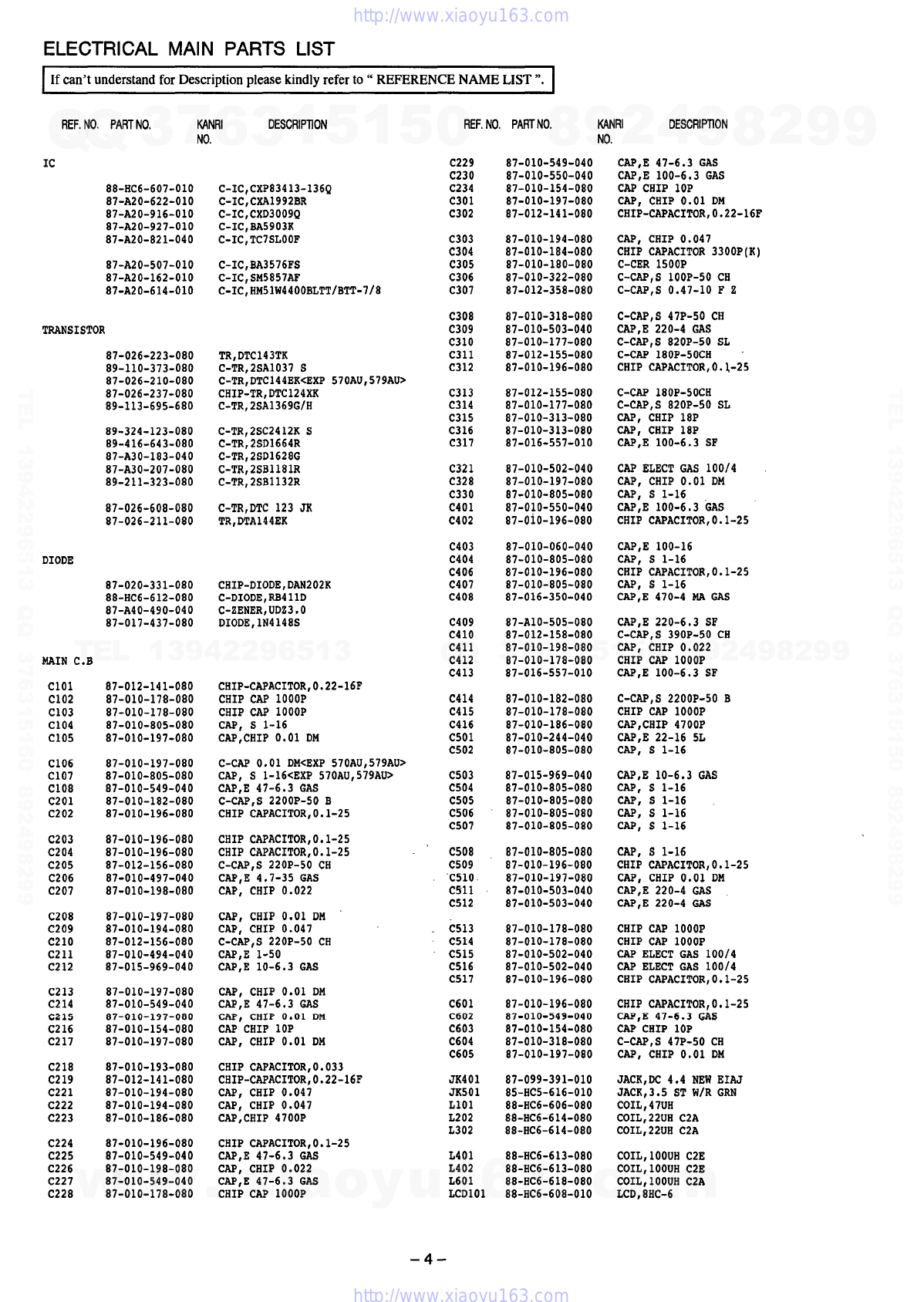
Ic
Ic,
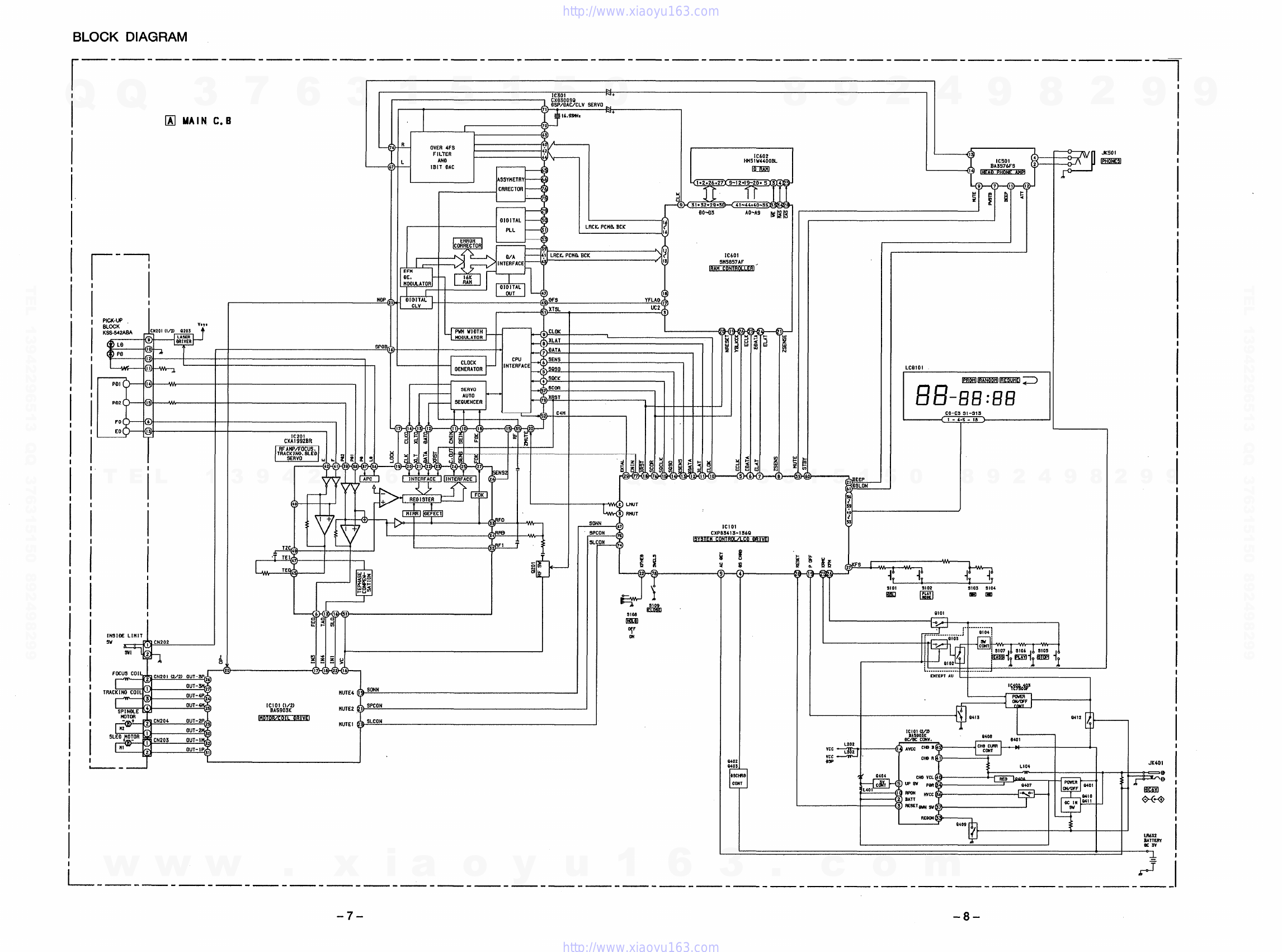
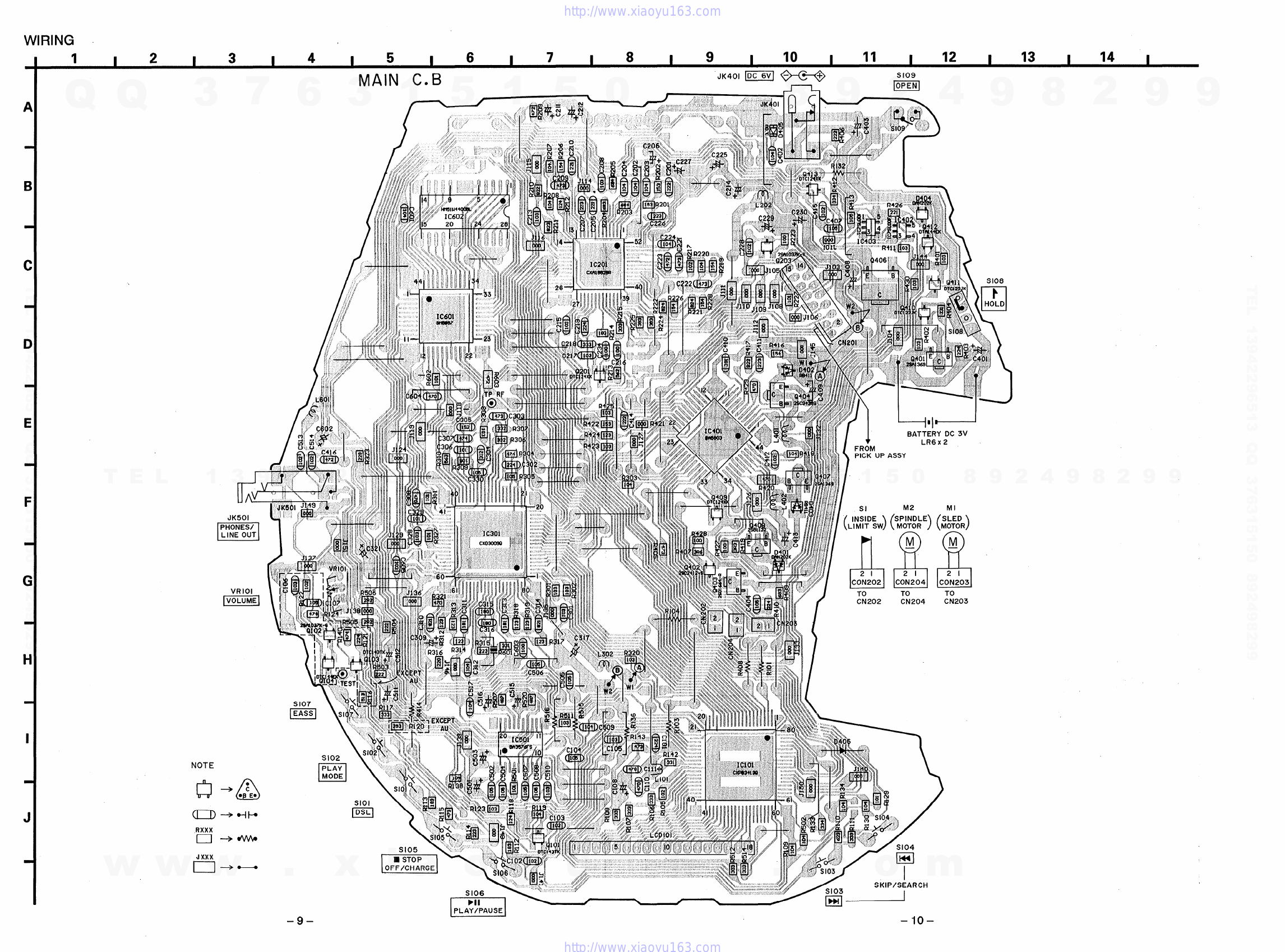
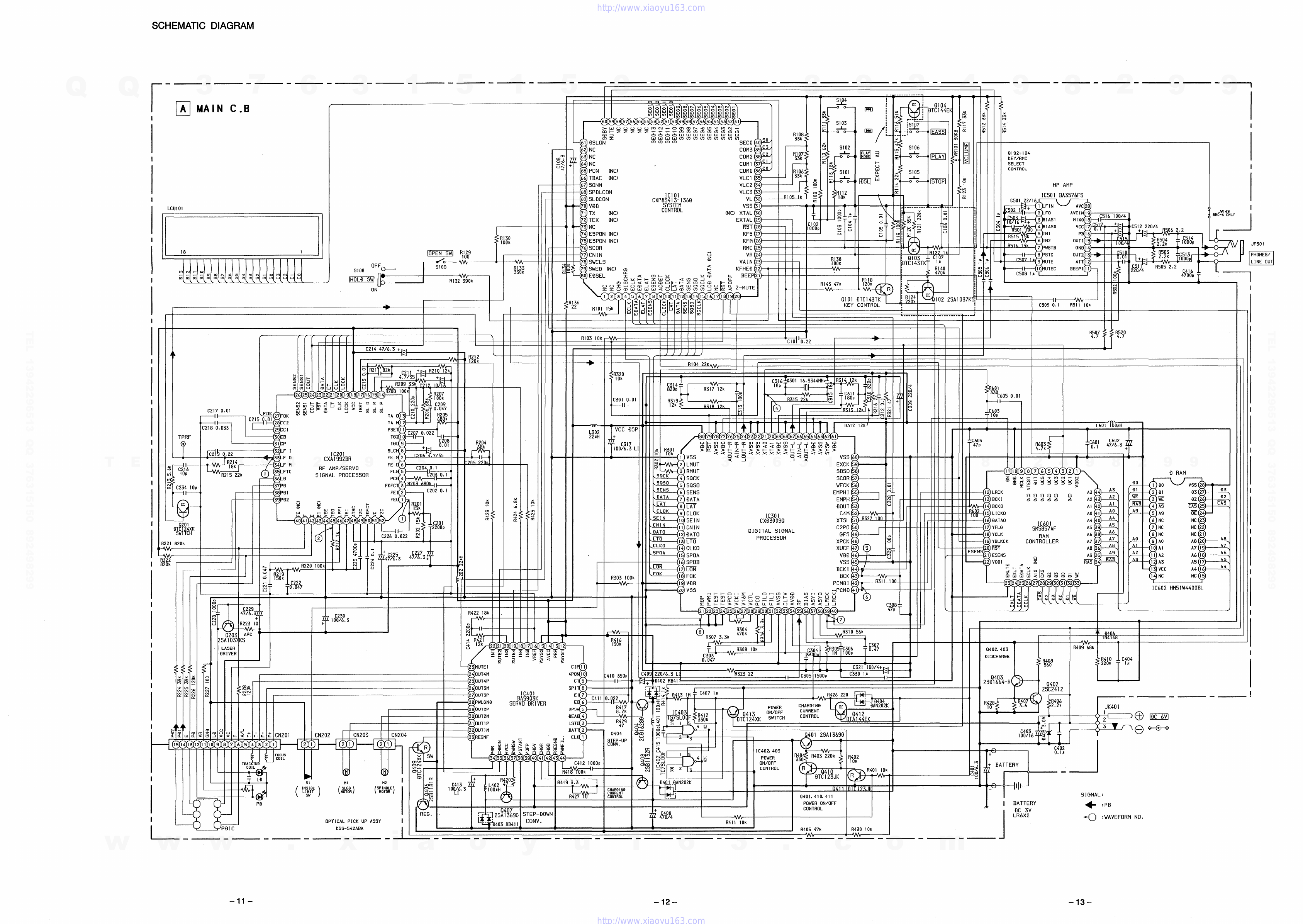
BLOCKDIAGRAM
BA3576FS
WAVEFORM IC DESCRIPTION
IC.CXD30090
d)IC201Pin@VOLT/DIV:0.5V
TIME/DIV:1K@lc301pin@f=2.1168MHz PinNo. PinName 1/0 Description
1Vss GND.
2LMUT oLeft
channelzerodetectingflag.
3RMUT oRightchannelzerodetectingflag.
4SQCK ISQSOreadoutclockinput.
5SQSO oSubQ80-bitserialoutput.
6SENS oSENSoutputtoCPU.
7DATA ISerialdatainputfkomCPU.
8GILatchinputfromCPU.Serialdataislatchedatthefallingedge.
9CLOK ISerialdatatransferclockinputfromCPU.
---
10 SEIN 1SENSinputfromSSP.
11 CNIN ITrackjumpcountsignalinput.
12 DATO oSerialdataoutputtoSSP.
13 LTO o’ SerialdatalatchoutputtoSSP.Latchedatthefallingedge.
14 CLKO oSerialdatatransferclockoutputtoSSP.
15 SPOA IMicrocomputerextendedinterface(inputA).
16 SPOB IMicrocomputerextendedinterface(inputB).
17 LON oMicrocomputerextendedinterface(output).
18 FOK IFocusOKinput.UsedforSENSoutputandtheservoautosequencer.
19 VDD Powersupply(+3V).
20 Vss GND.
21 MDP oSpindlemotorservocontrol.
22 PWMI ISpindlemotorexternalcontrolinput.ConnectedtoGND.
23 TEST ITestpin.ConnectedtoGND.
24 TEST ITestpin.ConnectedtoGND.
25 VPCO oChargepumpoutputforthewide-bandEFMPLL.
26 VCKI IVC02oscillationinputforthewide-bandEFMPLL.
27 V16M oVC02oscillationoutputforthewide-bandEFMPLL.
28 VCTL IVC02controlvoltageinputforthewide-bandEFMPLL.
29 Pco oMasterPLLfilteroutput.
30 FILO oMasterPLLfilteroutput.
31 FILI IMasterPLLfilterinput.
32 AVSS AnalogGND.
33 CLTV IMasterVCOcontrolvoltageinput.
34 AVDD Analogpowersupply(+3V).
35 RF IEFMsignalinput.
36 BIAS IConstantcurrentinputoftheasymmetrycircuit.
37 ASYI IAsymmetrycomparatorvoltageinput.
38 ASYO oEFMfull-swingoutput(low=VSS,high=VDD).
39 LRCK oD/Ainterface.LRclockoutputfrequency=Fs.
40 LRCKI ILRclockinput.
41 PCMD oD/Ainterface.Serialdataoutput(two’scomplmen~MSBfirst).
42 PCMDI ID/Ainterface.Serialdatainput(two’scomplment,MSBfirst).
43 BCK oD/Ainterface.Bitclockoutput.
@f=4,2MHz
R/F
Vc
RFIN
RFO
AVC
AVCIN
MIXO
Vcc
+B
OUT-R
GNB
OUT-L
ATT
BEEP I
------
I
I
I
I
I
I
I
1
I
I
I
I
I
I
I
I
I
I
I
I
I
I
onIlrIIiv
@IC301Pin(@@
@IC201Pin@VOLT/DIV:0,2V
TIME/DIV:50us VOLT/DIV:2V
TIME./DlV:0.2Ps
Vc
0.5V oJ3xKKIiv
I
I
BIAS —
.
.
.
—
—
—
I
I
I
Iu
Ln
t+
—
I
I
I
I
I
I
.
.
.
Vcc
w-
I
I1- aIC301Pin@
BIASO
IN-R
IN-L
PWSTB
PSTC
MUTE
MUTEC
@IC201Pin@)
I
IVOLT/DIV:O.lV
TIME/DIV:2ms VOLT/DIV:2V
;lM4~l);Vz5IIS
=.
I
I
I
I
I
I
I
I
+)3
T- Vc O.lv on_n_m8v
I
J
./
/
/
/
@
@IC301Pin@j) IC301Pin@VOLT/DIV:IV
TIME/DIV:5ILS
VOLT/DIV:IV
TIME/DIV:50ms
f=16.93MHz
&
3.3K 10K
I
I
I
I
I
I
I
I
I
I
I
I
I
I
I
I
I
I
I
I
I
I
I
I
I
I
I
I
I
I
L----- ----- ---- -ATT
BEEP
4
2.8V
Vc 111111111111
S8:8891lm919
allaaae18111
.5V
r
—
3.3K 1OK
0’ 1.4V
-14- –15– -16–
w
w
w
.
x
i
a
o
y
u
1
6
3
.
c
o
m
Q
Q
3
7
6
3
1
5
1
5
0
9
9
2
8
9
4
2
9
8
T
E
L
1
3
9
4
2
2
9
6
5
1
3
9
9
2
8
9
4
2
9
8
0
5
1
5
1
3
6
7
3
Q
Q
TEL 13942296513 QQ 376315150 892498299
TEL 13942296513 QQ 376315150 892498299
http://www.xiaoyu163.com
http://www.xiaoyu163.com