AT-START-F403 User Manual
2019.12.25 10 Rev 1.3
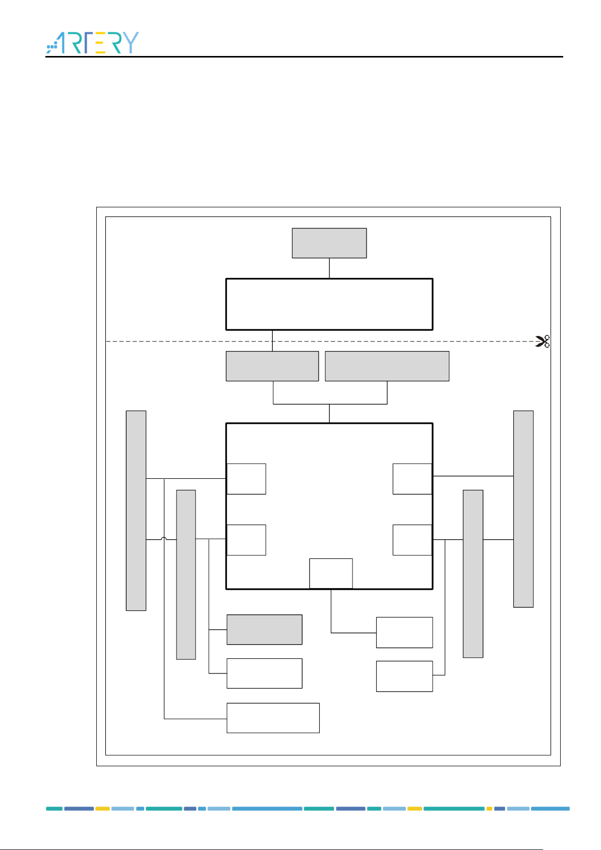
4.1 Programming and debugging
4.1.1 Embedded AT-Link-EZ
The evaluation board embeds Artery AT-Link-EZ programming and debugging tool for users to
program/debug the AT32F403ZGT6 on the AT-START-F403 board. AT-Link-EZ supports SWD
interface mode and a set of virtual COM port (VCP) to be connected to the
USART1_TX/USART1_RX (PA9/PA10) of AT32F403ZGT6. In this case, PA9 and PA10 of
AT32F403ZGT6 will be affected by AT-Link-EZ as follows:
PA9 is weakly pulled up to high level by the VCP RX pin of AT-Link-EZ;
PA10 is strongly pulled up to high level by the VCP TX pin of AT-Link-EZ
The user can set R16 and R24 OFF, then the use of PA9 and PA10 of AT32F403ZGT6 is not
subject to the above restrictions.
Please refer to AT-Link User Manual for complete details on the operations, firmware upgrade and
precautions of AT-Link-EZ.
The AT-Link-EZ PCB on the evaluation board can be separated from AT-START-F403 by bending
over along the joint. In this case, AT-START-F403 can still be connected the CN7 of AT-Link-EZ
through CN2 (not mounted before shipping), or can be connected with another AT-Link to continue
the programming and debugging on the AT32F403ZGT6.
4.1.2 20-pin ARM® standardJTAG connector
AT-START-F403 also reserves JTAG or SWD general-purpose connectors as
programming/debugging tool. If the user want to use this interface to program and debug the
AT32F403ZGT6, please seperate the AT-Link-EZ from the board or set R41, R44 and R46 OFF,
and connect the CN3 (not mounted before shipping) to the programming and debugging tool.
4.2 Power supply selection
The 5 V power supply of AT-START-F403 can be provided throug a USB cable (either through the
USB connector CN6 on the AT-Link-EZ or USB connector CN1 on the AT-START-F403), or
through an external 5 V power supply (E5V), or by an external 7~12 V power supply (VIN) via 5V
voltage regulator (U1) on the board. In this case, the 5 V power supply provides the 3.3 V power
required by the microcontrollers and peripherals by means of the 3.3 V voltage regulator (U2) on
the board.
The 5 V pin of J4 or J7 can also be used as an input power source. The AT-START-F403 board
must be powered by a 5 V power supply unit.
The 3.3 V pin of J4 or the VDD pin of J1 and J2 can also be directly used as 3.3 V input power
supply. AT-START-F403 board must be powered by a 3.3 V power supply unit.
Note: Unless 5 V is provided through the USB connector (CN6) on the AT-Link-EZ, the AT-Link-EZ will
not be powered by other power supply methods.
When another application board is connected to J4, the VIN, 5 V and 3.3 V pins can be used as
output power; the 5 V pin of J7 used as 5 V output power; the VDD pin of J1 and J2 used as 3.3 V
output power.