ARTERY AT32F415 Series User manual

Getting Started with AT32F415
2022.10.21 1 Ver 2.0.3
AN0022
Application Note
Getting Started with AT32F415
Introduction
This application note is written to help users with rapid project development using AT32F415xx.
Note: The corresponding code in this application note is developed on the basis of V2.x.x BSP provided by
Artery. For other versions of BSP, please pay attention to the differences in usage.
Applicable products:
Part number
AT32F415xx

Getting Started with AT32F415
2022.10.21 2 Ver 2.0.3
Contents
1Preliminary environment requirements...........................................................6
1.1 Build AT32 development environment.............................................................................6
1.1.1 Debug tools and evaluation board............................................................................6
1.1.2 Programming tools and software..............................................................................6
1.1.3 AT32 development environment...............................................................................7
1.1.4 How to replace SXX...............................................................................................12
1.2 AT32F415 chip enhanced functions..............................................................................13
1.2.1 Prefetch buffer.......................................................................................................13
1.2.2 PLL clock settings..................................................................................................14
1.2.3 Encryption mode....................................................................................................16
1.2.4 Set boot memory as main Flash memory extension area.......................................19
1.2.5 Recognize AT32 MCUin program..........................................................................22
2FAQs in downloading/compiling...................................................................24
2.1 Hard Fault Handler..........................................................................................................24
2.2 J-Link cannot find IC .......................................................................................................24
2.3 Problems in program downloading................................................................................24
2.3.1 Error: Flash Download failed–“Cortex-M4” .............................................................24
2.3.2 No Debug Unit Device found..................................................................................25
2.3.3 RDDI-DAP Error.....................................................................................................25
2.3.4 ISP serial port gets stuck in downloading...............................................................25
2.3.5 Resume download.................................................................................................25
3Security Library (sLib) ..................................................................................28
3.1 Introduction......................................................................................................................28
3.2 Principles of application..................................................................................................28
3.3 Security library application .............................................................................................28
4Revision history............................................................................................ 29

Getting Started with AT32F415
2022.10.21 4 Ver 2.0.3
List of figures
Figure 1. AT-START-F415 evaluation board with AT-Link-EZ......................................................... 6
Figure 2. AT-START-F415 evaluation board package...................................................................... 6
Figure 3. ICP/ISP/AT-Link-Family.................................................................................................... 7
Figure 4. BSP package................................................................................................................... 7
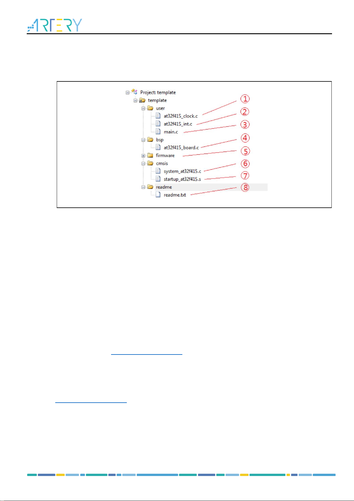
Figure 5. Keil_v5 templates............................................................................................................ 8
Figure 6. Pack download................................................................................................................ 9
Figure 7. Set up ArteryTek.AT32F415 _DFP................................................................................... 9
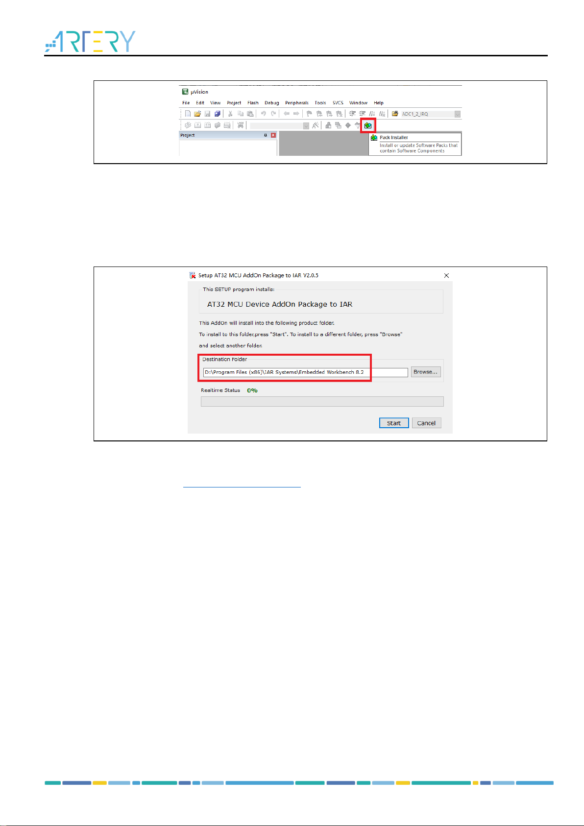
Figure 8. Set up Keil4_AT32MCU_AddOn ...................................................................................... 9
Figure 9. Pack Installer icon in Keil............................................................................................... 10
Figure 10. Set up IAR_AT32MCU_AddOn .................................................................................... 10
Figure 11. Keil Debug option..........................................................................................................11
Figure 12. Keil Debug Settings......................................................................................................11
Figure 13. Keil Utilities...................................................................................................................11
Figure 14. IAR Debug option ........................................................................................................ 12
Figure 15. IAR CMSIS-DAP option ............................................................................................... 12
Figure 16. Wait states of Flash performance select register (FLASH_PSR) .................................. 13
Figure 17. System clock configuration function “system_clock_config”.......................................... 13
Figure 18. AT32F415 150 MHz PLL clock configuration................................................................ 14
Figure 19. SXXPLL auto step-by-step switch configurations......................................................... 15
Figure 20. AT32 PLL auto step-by-step switch configurations........................................................ 15
Figure 21. Enable/disable access protection in ISP Programmer .................................................. 16
Figure 22. Enable access protection in ISP Programmer .............................................................. 17
Figure 23. Disable access protection in ISP Programmer.............................................................. 17
Figure 24. Enable erase and program protection in ICP Programmer ........................................... 18
Figure 25. Disable erase and program protection in ICP Programmer........................................... 19
Figure 26. Set AP mode in ICP Programmer................................................................................. 20
Figure 27. AP mode enabling in ICP Programmer......................................................................... 20
Figure 28. Offline config settings in ICP Programmer.................................................................... 21
Figure 29. AT-Link project file settings........................................................................................... 22
Figure 30. AT-Link offline download status.................................................................................... 22
Figure 31. Read Cortex ID............................................................................................................ 23
Figure 32. Read PID and UID ....................................................................................................... 23
Figure 33. Flash Download failed–“Cortex- M4” pops up in downloading...................................... 24

Getting Started with AT32F415
2022.10.21 5 Ver 2.0.3
Figure 34. Operate ConfigJLink_V1.0.0 in KEIL............................................................................ 26
Figure 35. ConfigJLink_V1.0.0 execution progress in KEIL ........................................................... 26
Figure 36. Operate ConfigJLink_V1.0.0 in IAR.............................................................................. 27
Figure 37. ConfigJLink_V1.0.0 execution progress in IAR............................................................. 27

Getting Started with AT32F415
2022.10.21 6 Ver 2.0.3
1 Preliminary environment requirements
Download development environment
ARTERY's officialwebsite
1.1 Build AT32 development environment
1.1.1 Debug tools and evaluation board
The AT32F415 evaluation board has an AT-Link-EZdebug tool, as shown in the red box in Figure 1
below. The AT-Link-EZ can be disassembled and used with other circuit boards, supporting IDE
online debugging, online programming and USB-to-serial port.
Figure 1. AT-START-F415 evaluation board with AT-Link-EZ
Note: For details about resources for AT-START evaluation board, please refer to
UM_AT_START_F415_Vx.x. Path: ARTERY’s official website→PRODUCTS→Value line→AT32F4xx;
download and unzip Evaluation Board package, and get the “\AT_START_F415_Vx.x\03_Documents”.
Figure 2. AT-START-F415 evaluation board package
1.1.2 Programming tools and software
AT programming tools and software: AT-Link / AT-Link+ /AT-Link-Pro / AT-Link-ISO /AT-Link-
7-12 V externalpow er socket
Boot mode select (BOOT jumper cap)
20-pin ARM
Standard
JTAG port
AT-Link port
User LED*3
I/O extendport
USART1 port
USB Host
port
USB OTG
port
RESET
button
USER
button
GPIO andUSB OTG jumper cap
ArduinoUno extendport

Getting Started with AT32F415
2022.10.21 7 Ver 2.0.3
EZ, ICP/ISP.
3rd party programming tools: J-Link, Armfly, Alientek, XWOPEN, ICWORKSHOP, ZLG,
MaxWiz, Amomcu, Acroview, Forcreat, Galecomm, Prosystems, Rx-prog, Sinaen, XELTEK,
Zhifeng, etc.
Note: For more information, please visit ARTERY’s official website→SUPPORT→Hardware Development
Tool and 3RD Party Writer.
For ICP usage instructions, please refer to UM_ICP_Programmer. Path: ARTERY’s official
website→PRODUCTS→Value line→AT32F4xx; download and unzip ICP tool, and get the
“Artery_ICP_Programmer_Vx.x.xx\Document\UM_ICP_Programmer”.
For ISP usage instructions, please refer to UM_ISP_Programmer. Path: ARTERY’s official
website→PRODUCTS→Value line→AT32F4xx; download and unzip ISP tool, and get the
“Artery_ISP_Programmer_Vx.x.xx\Document\UM_ISP_Programmer”.
ForAT-Link usage instructions, please refer to UM0004_AT-Link_User_Manual.
Path: ARTERY’s official website →PRODUCTS →Value line →AT32F4xx; download and
unzip AT-Link-Family, and get the “AT_Link_CH_ Vx.x.x\05_Documents\UM0004_AT-
Link_User_Manual_ZH_Vx.x.x”.
Figure 3. ICP/ISP/AT-Link-Family
1.1.3 AT32 development environment
1.1.3.1 Templateprojects
The commonly used IDE template projects are available from BSP provided by ArteryTek. BSP
path: ARTERY’s official website→PRODUCTS→Value line→AT32F4xx.
Figure 4. BSP package
The template projects of Keil_v5/Keil_v4/IAR_6.10/IAR_7.4/IAR_8.2/eclipse_gcc/at32_ide are

Getting Started with AT32F415
2022.10.21 8 Ver 2.0.3
created in BSP. Path: AT32F415_Firmware_Library_V2.x.x\project\at_start_f4xx\templates. Open
the project folder and click on the project file to open the corresponding IDE project. The example
of Keil_v5 template project is shown below.
Figure 5. Keil_v5 templates
Contents in the project:
①at32f415_clock.c:clockconfigurationfile, containsdefault clock frequencyandclock path;
②at32f415_int.c: interrupt file, part of core interrupt function code flow is written by default;
③main.c: main code file of the template project;
④at32f415_board.c: board-level configuration file, contains settings of AT-START on-board
buttons and LEDs;
⑤at32f415_xx.c under firmware: driver file of on-chip peripherals;
⑥system_at32f415.c: system initialization file;
⑦startup_at32f415.s: startup file;
⑧readme.txt: project documentation, contains application functions, setting methods and
associated application notes (ApNote) of the template project.
Except for templates, BSP also includes code examples (Keil_v5 project files) in terms of
peripherals for reference (AT32F415_Firmware_Library_V2.x.x\project\at_start_f4xx\examples).
Note: For more details about BSP, please refer to “Section 4 BSP application” of AT32F415 Firmware
BSP&Pack User Guide. Path: ARTERY’s official website→PRODUCTS→Value line→AT32F4xx; download
and unzip BSP, and get the “\AT32F415_Firmware_Library_Vx.x.x\document”.
1.1.3.2 Packinstallation
Install Pack and add the AT32 MCU part number to Keil/IAR. You can download Pack from
ARTERY’s official website→PRODUCTS→Value line→AT32F4xx.

Getting Started with AT32F415
2022.10.21 9 Ver 2.0.3
Figure 6. Pack download
For Keil compiling system, keil 4.74 /5.23 or above is recommended. If Keil_v5 is used, please
unzip Keil5_AT32MCU_AddOn and installthe correspondingArteryTek.AT32F415_DFP. If Keil_v4
is used, please install Keil4_AT32MCU_AddOn. By default, the Keil installation path can be
recognized automatically during installation. If the path is not recognized or incorrect, you need to
manually select the Keil installation path.
Figure 7. Set up ArteryTek.AT32F415 _DFP
Figure 8. Set up Keil4_AT32MCU_AddOn
You can also open keil and click on “Pack Installer” icon; then click on the top left “file” and select
“import” to import the corresponding pack downloaded from ARTERY's official website.

Getting Started with AT32F415
2022.10.21 10 Ver 2.0.3
Figure 9. Pack Installer icon in Keil
For IAR compiling system, IAR7.0 or IAR6.1 above is recommended. It is necessary to install
IAR_AT32MCU_AddOn. By default, the IAR installation path can be recognized automatically during
installation. If the path is not recognized or incorrect, you need to manuallyselect the IAR installation
path.
Figure 10. Set up IAR_AT32MCU_AddOn
Note: For more details about Pack setup, please refer to “Section 2 Pack setup” of AT32F415 Firmware
BSP&Pack User Guide. Path: ARTERY’s official website→PRODUCTS→Value line→AT32F4xx; download
and unzip BSP, and get the “\AT32F415_Firmware_Library_Vx.x.x\document”.
1.1.3.3 Use AT-Linkfor debugand download
If you want to use AT-Link in IAR, select CMSIS-DAP in Debugger option.

Getting Started with AT32F415
2022.10.21 11 Ver 2.0.3
Figure 11. Keil Debug option
Go to Debug and click on Settings to enter the Cortex-M Target Driver Setup interface.
1. Select AT-Link(WinUSB)-CMSIS-DAP/AT-Link-CMSIS-DAP;
Note: For details about WinUSB, please refer to FAQ0136_How to use AT-LINKWinUSB to improve download
speed (ARTERY’s official website→SUPPORT→FAQ→FAQ0136).
2. Find Port, select SW and then tick SWJ;
3. Confirm that the ARM SW-DP debug module is recognized.
Figure 12. Keil Debug Settings
Click on Utilities and untick option box 1; then select CMSIS-DAP Debugger in option box 2, and
finally tick option box 1 (it should be unticked first and then ticked).
Figure 13. Keil Utilities

Getting Started with AT32F415
2022.10.21 12 Ver 2.0.3
If you want to use AT-Link in IAR, please click on Project and select Options; then select CMSIS-
DAP in Debugger option, and select SWD in CMSIS DAP option.
Figure 14. IAR Debug option
Figure 15. IAR CMSIS-DAP option
Note: For details about Flash algorithm file, MCU switch and solutions for “J-Link cannot find MCU”, please
refer to AT32F415 Firmware BSP&Pack User Guide. Path: ARTERY’s official website→PRODUCTS→Value
line→AT32F4xx; download and unzip BSP, and get the “\AT32F415_Firmware_Library_Vx.x.x\document”.
1.1.4 How to replace SXX
Please refer to MG0005_ Migrating fromSXX32F0xx&GX32F3x0 to AT32F415 (ARTERY’s

Getting Started with AT32F415
2022.10.21 13 Ver 2.0.3
officialwebsite→PRODUCTS→Value line→AT32F4xx);
If the programstill cannot run properly after completing the above steps, please refer to other
sections of this application note or contact the agent and ARTERY technicians for help.
Note: Compared with SXX32F0xx, AT32F415 is more flexible to achieve better performance. Please refer to
AN0004_Performance_Optimization (ARTERY’s official website→SUPPORT→AP Note→AN0004) to learn
how to promote performance of AT32F415.
1.2 AT32F415 chip enhanced functions
1.2.1 Prefetch buffer
When the prefetch buffer is set, the CPU can execute operations faster. For example, while the
CPU is reading one byte, the next byte is waiting in the prefetch buffer. The Prefetch controller
decides whether to access the Flash according to the available space in the prefetch buffer. When
there is at least one available block in the prefetch buffer, the prefetch controller starts a read
operation.
The user needs to set wait states according to different systemclock frequencies by setting bit 2:0
of the FLASH_PSR register (corresponds to the FLASH_ACR register of SXX32).
Figure 16. Wait states of Flash performance select register (FLASH_PSR)
AT library has corresponding settings in the system clock configuration function
“system_clock_config()”. For other BSP versions, please find out the correct position and complete
the corresponding settings.
Figure 17. System clock configuration function “system_clock_config”
Note: When the AHB clock prescaler is not equalto 1, the Flash prefetch buffer (FLASH_PSR[4]=0x1) must
be enabled.

Getting Started with AT32F415
2022.10.21 14 Ver 2.0.3
1.2.2 PLL clock settings
1.2.2.1 PLLsetting methods
The embedded PLL clock of AT32F415 has a maximum output frequency of 150 MHz, and it can be
configured by using the CRM_CFG register (corresponds to the RCC_CFGR register of SXX32) or
the additional CRM_PLL register. Users can use the CRM_PLL register to configure more PLL clock
frequencies, and the formula is shown below:
PLL output clock = PLL ref. input clock × PLL multiplication factor (PLL_NS)
PLL pre − division factor (PLL_MS) × PLL post− division factor (PLL_FR)
When the SXX32F0xx BSP is used, the PLL setting example (HEXT=8 MHz, PLL=48 MHz):
RCC->CFGR|= (uint32_t)(RCC_CFGR_PLLSRC_HSE|RCC_CFGR_PLLMULL6);
If the user wants to use SXX32F0xx programto output a clock greater than 48 MHz on AT32F415, it
is necessaryto configurethe CRM_CFG register(correspondstothe RCC_CFGR registerof SXX32).
When PLL=144 MHz, the corresponding setting is as follows:
RCC->CFGR|= (uint32_t)(RCC_CFGR_PLLSRC_HSE|RCC_CFGR_PLLMULL18);
When the AT BSP is used, the PLL setting example (HEXT=8 MHz, PLL=48 MHz):
crm_pll_config(CRM_PLL_SOURCE_HEXT,CRM_PLL_MULT_6);
When the AT BSP is used, the PLL setting example (HEXT=8 MHz, PLL=144 MHz):
crm_pll_config(CRM_PLL_SOURCE_HEXT,CRM_PLL_MULT_18);
The user also can use the additional CRM_PLL register of AT32 MCU to configure more clock
frequencies. For example, if the AT32F415 BSP is used, the PLL setting example (HEXT=8 MHz,
PLL=150 MHz):
Figure 18. AT32F415 150 MHz PLL clock configuration
#define CRM_PLL_NS ((uint16_t)0x4B) /* PLL_NS=75*/
#define CRM_PLL_MS ((uint16_t)0x01) /* PLL_MS=1 */
/* config pllclock resource PLL_FR =4*/
crm_pll_config2(CRM_PLL_SOURCE_HEXT,CRM_PLL_NS,CRM_PLL_MS, CRM_PLL_FR_4);
Where, the parameter CRM_PLL_SOURCE_HEXT represents that the HEXT is used as external
clock source; PLL_NS=75, PLL_MS=1, and CRM_PLL_FR_4 (0x02, divided by four) represents the
PLL_FR value.
Please refer to AN0117_AT32F415_CRM_Start_Guide (ARTERY's official website→SUPPORT
→AP Note→AN0117) for more details about AT32F415 clock source settings and modification and
learn how to use New Clock Configuration (ARTERY's official website→PRODUCTS→Value
line→AT32F4xx) to generate the desired clock code and apply it to the project.

Getting Started with AT32F415
2022.10.21 15 Ver 2.0.3
1.2.2.2 Auto step-by-stepswitch
When the internal PLL of AT32F415 is set to 108 MHz and above, it is necessary to performauto
step-by-step switch.
When the SXX32F0xx BSP is used, the user needs to open system_sxx32f0xx.c and find out the
current system clock configuration function (go through Section 1.2.2.1 PLL settings), and add the
following codes in Italic black to the static void SetSysClockToxxM(void) function.
Figure 19. SXX PLL auto step-by-step switch configurations
/* Wait tillPLL is ready*/
while((RCC->CR&RCC_CR_PLLRDY)== 0)
{
}
*((unsigned int *)0x40021054)|= (0x30); // Enable auto step-by-step clock switchfunction
/* Select PLL as system clocksource*/
RCC->CFGR&= (uint32_t)((uint32_t)~(RCC_CFGR_SW));
RCC->CFGR|= (uint32_t)RCC_CFGR_SW_PLL;
/* Wait tillPLL is usedas system clocksource */
while((RCC->CFGR& (uint32_t)RCC_CFGR_SWS)!= (uint32_t)0x08)
{
}
*((unsigned int *)0x40021054)&=~(0x30); // Disable auto step-by-step clock switch function
When the AT32F415 BSP is used, the example of PLL auto step-by-step switch is shown below:
Figure 20. AT32 PLL auto step-by-step switch configurations
/* enableautostepmode*/
crm_auto_step_mode_enable(TRUE);
/* selectpllas system clocksource */
crm_sysclk_switch(CRM_SCLK_PLL);
/* wait till pllis used as system clocksource*/
while(crm_sysclk_switch_status_get()!= CRM_SCLK_PLL)
{
}
/* disableautostepmode*/
crm_auto_step_mode_enable(FALSE);
/* updatesystem_core_clockglobalvariable */
system_core_clock_update();
Note: If the auto step-by-step systemclock switch is enabled, it must be disabled after clock switch.

Getting Started with AT32F415
2022.10.21 16 Ver 2.0.3
1.2.3 Encryption mode
1.2.3.1 Accessprotection
The access protection is commonly known as “encryption”, which is applied to the entire Flash
storage area. Once the Flash access protection is enabled, the embedded Flash storage area can
only be read through normal execution of the program, not through JTAG or SWD. When ICP/ISP
tool is used to disable the access protection, the chip will performerase operation on the Flash.
Note: Once enabled, the high-level accessprotection cannot be disabled, and the user is not allowed to
re-erase or program the system data area in any way.
The ICP/ISP tool can be used to enable and disable IC access protection, as shown below:
Artery ICP Programmer (BOOT0=0, BOOT1=0)
Enable access protection: Open Artery ICP Programmer—Access protection—Enable high-
level access protection.
Disable access protection: Open Artery ICP Programmer—Access protection—Disable.
Figure 21. Enable/disable access protection in ICP Programmer
Artery ISP Programmer (BOOT0=1, BOOT1=0)
Enable access protection: Click on “Next” until enter the final interface, then select
“Protection/Enable/Access protection” —Next—Yes, encrypted.
Disable access protection: Protection/Disable/Access protection—Next—Yes, Flash decrypted.

Getting Started with AT32F415
2022.10.21 17 Ver 2.0.3
Figure 22. Enable access protection in ISP Programmer
Figure 23. Disable access protection in ISP Programmer
Artery ISP Multi-Port Programmer (BOOT0=1, BOOT1=0)
Enable access protection: Protection/Enable/High-level access protection—Start, encrypted;
Disable access protection: Protection/Disable/Access protection—Start, Flash decrypted.
Note: Once enabled, the access protection cannot be disabled through erase operation.

Getting Started with AT32F415
2022.10.21 18 Ver 2.0.3
1.2.3.2 Eraseandprogramprotection
The programprotection is applied to the entire Flash storage area or certain pages in the Flash
storage area. Once the Flash programprotection is enabled, the internal Flash storage area cannot
be programmed in any way.
The user can use ICP/ISP programmer to enable/disable erase and programprotection, as shown
below:
Artery ICP Programmer (BOOT0=0, BOOT1=0)
Enable erase and programprotection: Open Artery ICP Programmer—User system data—Tick
the sectors that require erase and programprotection—Apply to device.
Disable erase and programprotection: Open Artery ICP Programmer—User system data—
Untick the sectors that do not require erase and programprotection—Apply to device.
Artery ISP Programmer (BOOT0=1, BOOT1=0)
Enable erase and programprotection: Protection/Enable/Erase and programprotection—
Next—Yes, erase and programprotection enabled.
Disable erase and programprotection: Protection/Disable/Erase and programprotection—
Next—Yes, erase and programprotection disabled.
Artery ISP Multi-Port Programmer (BOOT0=1, BOOT1=0)
Enable erase and programprotection: Protection/Enable/Erase and programprotection—
Start—Yes, enabled.
Disable erase and programprotection: Protection/Disable/Erase and programprotection—
Start—Yes, disabled.
Figure 24. Enable erase and program protection in ICP Programmer

Getting Started with AT32F415
2022.10.21 19 Ver 2.0.3
Figure 25. Disable erase and program protection in ICP Programmer
Note: Once enabled, the erase and program protection cannot be disabled through erase operation.
1.2.4 Set boot memory as main Flash memory extension area
By default, boot memory stores the original boot codes in BOOT mode. For AT32F415 series MCUs,
the boot memory also can be used as the main Flash memory extension area (AP mode) to store
user-defined codes.
Note: The boot memory AP mode can only be set once, and the BOOT mode function of the original
boot memory cannot be restored after setting.
The user can use Artery ICP Programmer to set the boot memory as the main Flash memory
extension area as follows:
Connect AT-Link/J-Link emulator to AT-START-F415 board and power on;
Open Artery ICP programmer and select AT-Link/J-Link to connect;
Target—Boot memory AP mode—OK.

Getting Started with AT32F415
2022.10.21 20 Ver 2.0.3
Figure 26. Set AP mode in ICP Programmer
To prevent misoperations, the user needs to manually enter the enable key 0xA35F6D24, and
then the “Flash info” interface will display a success or failure message.
Figure 27. AP mode enabling in ICP Programmer
The user can use Artery ICP Programmer to set the boot memory as the main Flash memory
extension area (in mass production) as follows:
Connect AT-Link emulator to AT-START-F415 board and power on.
Note: The on-board AT-Link EZ does not support offline programming. If necessary, please use AT-Link other
than EZ version.
Other manuals for AT32F415 Series
1
Table of contents
Other ARTERY Motherboard manuals

ARTERY
ARTERY AT32-Video-EV User manual

ARTERY
ARTERY AT-START-F425 User manual

ARTERY
ARTERY AT-START-F403 User manual

ARTERY
ARTERY AT32-Comm-EV User manual

ARTERY
ARTERY AT-START-WB415 User manual

ARTERY
ARTERY AT32F4 Series User manual

ARTERY
ARTERY AT32F435 Series Specification sheet

ARTERY
ARTERY AT-START-F407 User manual

ARTERY
ARTERY AT-SURF-F437 User manual