AT-START-F425 User Manual
2021.10.20 9Rev 1.00
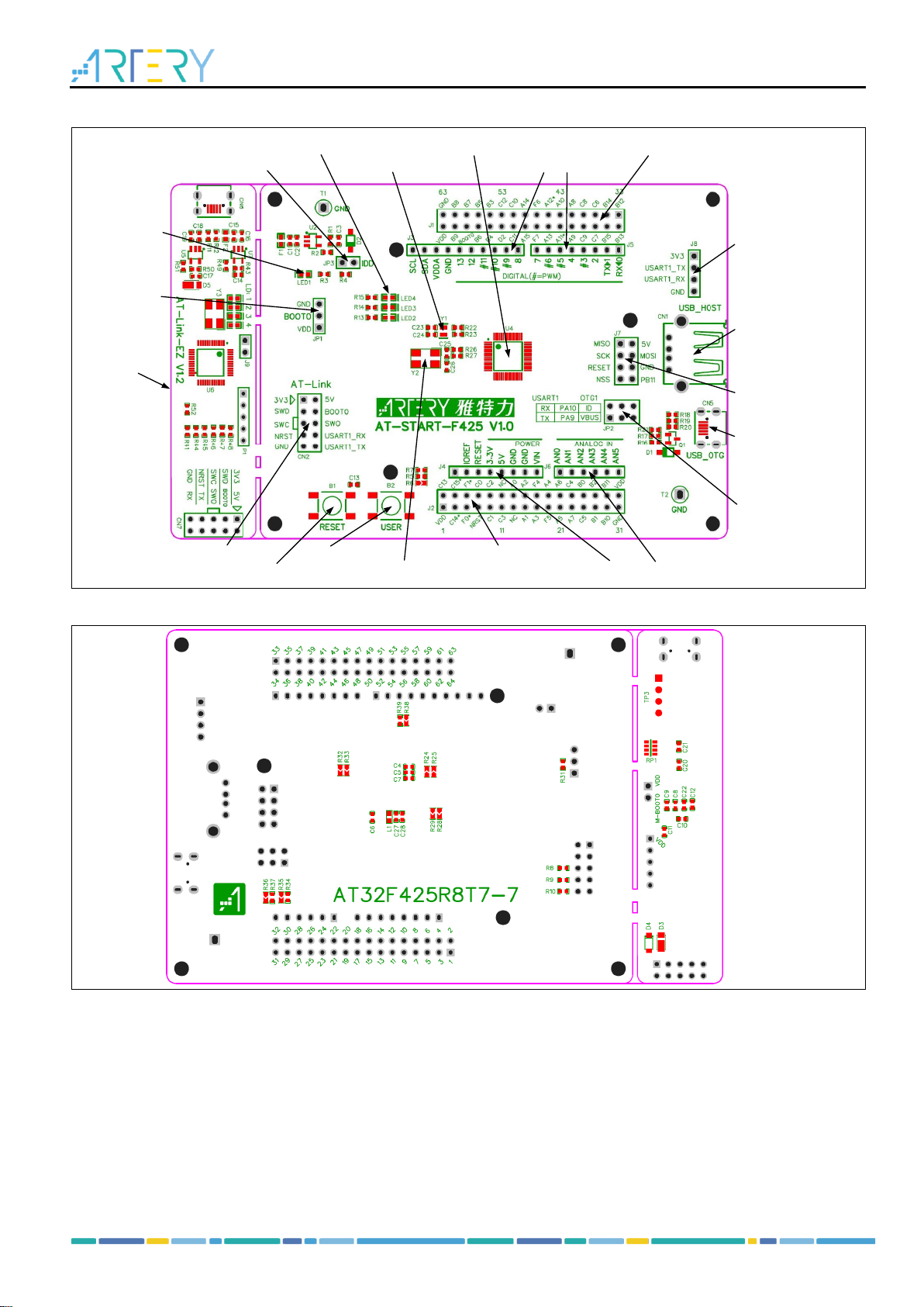
3.1 Power supply selection
The AT-START-F425 can not only be provided with 5 V through a USB cable (either through USB
connector CN6 on AT-Link-EZ or USB OTG connector CN5 on AT-START-F425), but also be
provided with an external 5 V power supply (E5V). Then 5 V power provides 3.3 V for the
microcontroller and its peripherals using on-board 3.3 V voltage regulator (U2).
5 V pin of J4 or J7 can also be used as an input power, so the AT-START-F425 board can be
supplied through a 5 V power unit.
The 3.3 V pin of J4, or the VDD of J1 and J2 can be used as 3.3 V input directly, so AT-START-
F425 board can also be supplied by a 3.3 V power unit.
Note: 5 V power supply must be provided through USB connector (CN6) on AT-Link-EZ. Any other
method cannot power the AT-Link-EZ.
When another board is connected to J4, 5 V and 3.3 V can be used output power, J7’s 5V pin as 5
V output power, the VDD pin of J1 and J2 as 3.3 V output power.
3.2 IDD
When JP3 OFF (symbol IDD) and R4 OFF, an ammeter can be connected to measure the power
consumption of AT32F425R8T7-7.
JP3 OFF, R4 ON:
AT32F425R8T7-7 is powered. (Default setting and JP3 plug is not mounted before shipping)
JP3 ON, R4 OFF:
AT32F425R8T7-7 is powered.
JP3 OFF, R4 OFF:
An ammeter must be connected to measure the power consumption of AT32F425R8T7-7. If
there is no ammeter available, the AT32F425R8T7-7 cannot be powered.
3.3 Programming and debugging: embedded AT-Link-EZ
The evaluation board integrates Artery AT-Link-EZ for users to program/debug the
AT32F425R8T7-7 on the AT-START-F425 board. AT-Link-EZ supports SWD interface mode, SWO
debug, and a set of virtual COM ports (VCP) to connect to the USART1_TX/USART1_RX
(PA9/PA10) of AT32F425R8T7-7.
Please refer to AT-Link User Manual for complete details on AT-Link-EZ.
The AT-Link-EZ on board can be disassembled or separated from the AT-START-F425. In this
case, the AT-START-F425 can still be connected to the CN7 interface (not mounted before leaving
factory) of AT-Link-EZ through CN2 interface (not mounted before leaving factory), or to AT-Link, in
order to continue to program and debug the AT32F425R8T7-7.