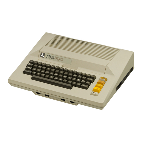
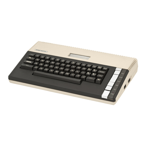
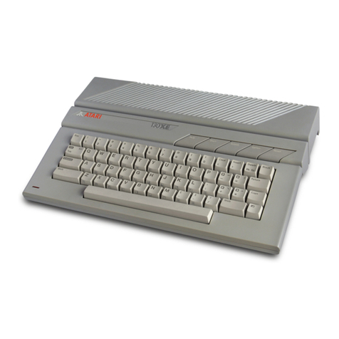
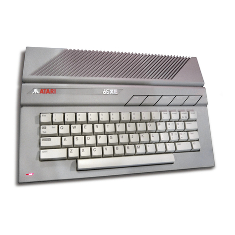
Atari 130XE User manual


TABLE OF CONTENTS
Section Title Page
INTRODUCTION IV
1 THEORY OF OPERATION 1-1
User Interface 1-2
Mechanical Description 1-3
Digital Hardware 1-5
6502 (Modified) CPU Microprocessor 1-5
Alphanumeric Television Interface Controller 1-6
(Antic Display Processor)
Graphics Television Interface Adaptor (GTIA) 1-7
POT Keyboard Integrated Circuit (POKEY) 1-8
Peripheral Interface Adaptor (PIA) 1-9
Memory (ROM and RAM) 1-11
Memory Management Unit (MMU) 1-11
RF Modulator 1-11
Power Supply 1-11
System Interface 1-11
Serial Input/Output (SIO Interface) 1-12
Keyboard Interface 1-13
Controller Jack Interface 1-14
Cartridge Interface 1-15
Monitor Interface 1-16
2 SCHEMATICS AND PICTURES 2-1
3 TESTING 3-1
Overview 3-1
Equipment Needed 3-1
Self Test 3-1
MEMORY TEST Screen 3-2
AUDIO VISUAL TEST Screen 3-2
KEYBOARD TEST Screen 3-3
ALL TESTS 3-3
Using the ATARI REV. 3.2 Production Test Cartridge 3-3
COLOR BAR TEST 3-6
ANY VIDEO TEST 3-7
GRAY BAR TEST 3-g
DISPLAY OPTIONS 3-9
RAM TEST 3-9
130XE Personal Computer
Field Service Manual I

TABLE OF CONTENTS (Cont.)
Section Title Page
4 SYMPTOM CHECKLIST 4-1
Adjustments & Replacements 4-2
Console Disassembly 4-2
Console Assembly 4-2
Keyboard Removal/Replacement 4-3
Color Adjustment 4-3
5 SERVICE BULLETINS 5-1
TABLE OF ILLUSTRATIONS
Figure Title Page
1-1 130XE Right Side Panel 1-1
1-2 130XE Back View 1-1
1-3 130XE Top View 1-2
1-4 130XE Functional Block Diagram 1-4
1-5 6502C CPU Pin Assignments 1-6
1-6 ANTIC Display Processor Pin Assignments 1-6
1-7 GTIA Pin Assignments 1-7
1-8 POKEY Pin Assignments 1-7
1-9 PIA Pin Assignments 1-8
1-10 Freddie Pin Assignments 1-8
1-11 External Power Supply Schematic 1-10
1-12 SIO Interface Pin Assignments 1-11
1-13 Controller Jack Interface Pin Assignments 1-11
1-14 Cartridge Slot Pin Assignments 1-12
1-15 Expansion Slot Pin Assignments 1-13
1-16 Monitor Jack Pin Assignments 1-13
2-1 Atari 130XE 16 X 4164 Assembly CO70065/CO70067 2-2
2-2 CO7065/CO70067 PCB 2-3
2-3 Atari 130XE SECAM CO70052 Rev. 2 PCB 2-4
2-4 Atari 130XE SECAM 2-5
2-5 Atari 130XE 4 X 4464 Assembly CA200519 2-6
130XE Personal Computer
Field Service Manual II

2-4 CA200519 PCB 2-7
2-5 Atari 65XE 8 X 4164 Assembly CO70025 2-8
2-6 CO70025 PCB 2-9
2-7 Atari 65XE 8 X 4164 Assembly CA20097 2-10
2-8 CA20097 PCB 2-11
2-9 Atari 65XE/800XE 2 X 4464 Assemblies CA200519 2-12
2-10 65XE/800XE CA200519 PCB 2-13
2-11 XE-System Assembly C100417 2-14
2-12 C100417 PCB 2-15
2-13 XE Keyboard Matrix 2-16
2-14 PCB and Shield Assemblies 2-17
3-1 SELF TEST Menu 3-1
3-2 MEMORY Test display 3-2
3-3 AUDIO-VISUAL Test display 3-2
3-4 KEYBOARD Test display 3-3
3-5 Select Screen 3-4
3-6 Main Menu display 3-4
3-7 AUDIO Test display 3-5
3-8 VIDEO Test display 3-6
3-9 PORT Test display 3-7
3-10 KEYBOARD Test display 3-8
3-11 ROM Test display 3-8
3-12 RAM Test 65XE OK. 3-9
3-13 RAM Test Fail 3-9
3-14 Cartridge & Expansion Slot Test Fixture 3-10
130XE Personal Computer
Field Service Manual III

INTRODUCTION
The Atari 130XE Personal Computer Field Service Manual is a reference guide for the service
technician. Since the XE series has more models, so on the basis of the 130XE model will
also be discussed different versions 65XE computers, as well as console XE-SYSTEM .
This Field Service Manual is organized in six sections:
•THEORY OF OPERATION – Overview of how the 130XE works and what its basic
assemblies look like.
•SCHEMATICS AND SILKSCREENS – Electrical drawings and layouts of the XE
series printed circuit board.
•TESTING – Review of Diagnostic Tests available for diagnosing 130XE problems.
•SYMPTOM CHECKLIST – Failure information to assist the experienced technician
arrive at a rapid diagnosis of XE series computers problems.
•PARTS LIST – Detailed breakdown of parts used in the XE computers.
•SERVICE BULLETINS – Section to be used to hold Field Change Orders, Upgrade
Bulletins and Tech Tips.
130XE Personal Computer
Field Service Manual IV

SECTION 1
THEORY OF OPERATION
The Atari 130XETM is an enhanced version of the existing Atari computer systems. It can be
used with any existing Atari peripheral devices which are compatible with the 400TM/800TM
or XL series computer, although not all are necessary.
The console contains 128K of RAM and has an operating system which contains one 16k X 8
ROM. The console also contains the keyboard with a HELP key, four programmable function
keys START, SELECT, OPTION, RESET, a single Cartridge slot, an Expansion connector,
jacks for adding peripherals and hand controllers, a detachable (RF) TV interface cable and
one power LED.
Use Figures 1-1, 1-2and 1-3 as reference for the following discussion.
Figure 1-1. 130XE Right Side Panel
Figure 1-2. 130XE Back View.
130XE Personal Computer
Field Service Manual 1-1

Figure 1-3. 130XE Top View
User Interface
The Atari XE series are a general purpose microcomputers which uses a 6502C
microprocessor. The 130XE console is the central processing unit for its respective system.
The right side panel (refer to Figure 1-1) contains two controller jacks. The controller jacks
accept the X-Y joystick and the paddle controllers available from Atari.
The rear panel (refer to Figure 2-1) contains the Serial Input/Output (SIO) jack, Cartridge slot,
the Expansion connector, the channel 2-3 switch, the RF cable jack, the Monitor jack, and the
Power Jack.
The console has a full stroke 62 key alphanumeric keyboard, which includes special
characters and controls, a space bar, and 5 function keys.
130XE Personal Computer
Field Service Manual 1-2

The 5 function keys above the keyboard are made of the same color material as cover. A
translucent plexiglass strip on left-bottom corner of top cover indicate the operation (Power
On) and covers the red LED.
From left to right the function keys are:
HELP – Gives you instruction in some programs when you need help.
START - Press to run loaded program. Frequently used to load program from cassette. Fully
programmable key
SELECT – Often used to select one of several applications within a program. Fully
programmable key.
OPTION – Allows the player to choose among the variations of a program. When this key is
pressed during Power On – internal Basic is disconnected and – if you do not
have active floppy drive – SELF TEST is running (see page 3-2). Fully programmable
key.
RESET – Interrupts and restarts the operating system or cartridge.
Mechanical Description
The 130XE computer console contains a single motherboard which houses all the chips of the
system and provides connectors for interfacing external modules to the console. It includes
the CPU, ANTIC, GTIA, POKEY, PIA, FREDDIE, RAM, ROM Operating System, and
includes all functions. The motherboard uses a common address bus, data bus and clock lines.
The sixteen-line address bus allows the microprocessor to directly address 64K of memory
locations. The eight-line data bus provides the communication and data path between the
functional modules. The various power requirements are routed from the power supply
throughout the console.
The keyboard is connected to the PC Board by a 24-conductor foil cable.
Figure 1-4 is a block diagram of the functional flow of the 130XE.
130XE Personal Computer
Field Service Manual 1-3
RF
Modulator
SIO
Keyboard
Expansion
Connector
Cartridge
Slot
MMU2
CO25953

RAM
MAIN 64k
RAM
BANK 64k
I/O
Joysticks
Paddles
A/V
Connector
FREDDIE
PIA
MMU1
CO61618
O.S.
ROM
BASIC
ROM
CPU
6502C
ANTIC
GTIA
POKEY
14MHz
Address Bus
Data Bus
Control Bus
RAM Addresses
SIO Signals
Function Keys
Other signals
Figure 1-4. 130XE Functional Block Diagram.
130XE Personal Computer
Field Service Manual 1-4

Digital Hardware
The digital hardware consists of:
•The 6502C CPU microprocessor
•The Alphanumeric Television Interface Controller (the ANTIC Display Processor)
•The Graphics Television Interface Adaptor (GTIA)
•The POT Keyboard Integrated Circuit (POKEY)
•The Peripheral Interface Adaptor (PIA)
•The Memory (ROM and RAM)
•Memory Management Units (MMU1 and MMU2)
•Clock and Memory Controller FREDDIE
6502C CPU Microprocessor
The 6502C (modified 6502) CPU microprocessor contains register flags, interconnections,
arithmetic logic, control logic, and all recognized operation codes. The characteristics of the
microprocessor are:
•Byte-oriented structure
•151 opcodes
•Decimal and binary arithmetic modes Seven addressing modes
•True indexing Stack pointer
•Two interrupt levels 64K address range
•Integral clock circuit
•Single +5 volt DC power Requirement
Figure 1-4 is an illustration of the 6502C CPU Pin Assignments.
130XE Personal Computer
Field Service Manual 1-5

Figure 1-5. 6502C CPU Pin Assignments.
Alphanumeric Television Interface Controller (The ANTIC Display Processor
The ANTIC Display Processor is a custom display microprocessor with an instruction set
customized for graphics generation. It also has the ability to control bus and RAM REFRESH.
Figure 1-6. Display Processor Pin Assignments
130XE Personal Computer
Field Service Manual 1-6

Graphics Television Interface Adaptor (GTIA)
The GTIA interfaces with the ANTIC processor on one side and with the video summation
circuitry on the other. Its primary task is to generate color and luminance signals from the
display information bit stream it receives from the ANTIC Display Processor.
Figure 1-7. GTIA pin assignments
POT Keyboard Integrated Circuit (POKEY)
The POKEY is a Custom Large Scale Integrated Circuit (LSI) chip. It is used for audio
generation, Serial Input/Output (SIO) control, controller interface scan and keyboard scan.
Figure 1-8. POKEY pin assignments
130XE Personal Computer
Field Service Manual 1-7

Peripheral Interface Adaptor (PIA)
The PIA is a general purpose Input/Output (I/O) chip.
Figure 1-9. PIA pin assignments
FREDDIE
Freddie is the controller of memory and generates a clock signal to CPU.
Figure 1-10. Freddie pin assignments
130XE Personal Computer
Field Service Manual 1-8

Memory
The 130XE operating system is resident to 16k X 8 ROM. The ROM input CPU address lines
A0 through A13 and the chip selects from the MMU, generates data on CPU data lines D0
through D7. RAM is organized as 16 X 64k x 1 or 4 X 64k X 4 chips, two for each data line.
48K RAM is directly available, but more is accessible under DOS 2.5.
Memory Management Unit (MMU)
The Memory Management (Address Decoding) circuitry consists of a Programmable Array
Logic (PAL) and one 3 to 8 decoder. The input to this circuitry are the address lines A8 thru
A15 and control signals like ROM enable (from PIA) and Refresh. The outputs of this
circuitry are GTIA chip select (D0XX), Expansion selects (D1XX), POKEY chip select
(D2XX), PIA chip select (D3XX), Cartridge selects (D5XX), O.S. ROM selects and RAM
selects.
The RF Modulator
The RF Modulator inputs the composite video from the video summation circuitry and the
monoaural audio signals and produces a modulated signal suitable for the television.
The modulated signal will have the following characteristics with a 75Ωtermination:
Maximum Voltage: 2 mV
Minimum Voltage: 1 mV
Audio Sound Carrier Frequency: 5.5 MHz
Frequency Response:
Ch. 3 61.25 MHz ± 0.5
Ch. 2 55.25 MHz
Power Supply
The 130XE has a external power supply. The power supply jack, power on switch and filters
are resident on the motherboard. The power supply accepts a 5V DC input through the power
jack. An external step-down transformer accepts 115V AC or 230V AC from the power line
and steps it down to 9VAC. The 9VAC input is rectified by a bridge rectifier and then
regulated power output from the regulator.
130XE Personal Computer
Field Service Manual 1-9

F1 T1
1 5
4 8
115/230V AC
5V DC
1
2
3
45
67
- +
D1
1
4
3
2
C2
100uF
U1
LM78S05
1
2
3
VIN
GND
VOUT
C1
4700uF
Figure 1-11. External Power Supply Schematic.
The DC output of regulator is 5V ±5% (1.5A Max).
SYSTEM INTERFACE
The 130XE provides the following interfaces:
•The Serial Input/Output (SIO) interface
•The keyboard interface
•The controller jack interface
•The cartridge interface
•The monitor interface
•The LED board interface
Serial Input/Output (SIO) Interface
The Atari 130XE communicates with peripheral devices over an asynchronous serial port
(19.2K Baud Rate Max). Data is transmitted and received as 8 bits of serial data (LSB sent
first) preceded by a logic zero start bit and succeeded by a logic one stop bit. The serial data
out is transmitted as positive logic. The serial DATA OUT line always assumes its new state
when the serial CLOCK OUT line goes high; CLOCK OUT goes low in the center of the
DATA OUT time.
The bus protocol specifies that all commands must originate from the computer, and that
peripherals present data on the bus only when commanded to do so. Every bus operation goes
to completion before another bus operation is initiated (no overlap). An error detected at any
point in the bus operation will abort the entire sequence. A bus operation consists of the
following elements:
Command Frame (From Computer)
Acknowledge Frame (From Peripheral)
Optional Data Frame (To or From Computer)
Complete Frame (From Peripheral)
130XE Personal Computer
Field Service Manual 1-10

Command Frame
The serial bus protocol provides for three types of commands:
1) Data Send
2) Data Receive
3) Immediate (No Data-Command Only)
PIN PIN
1 Clock In 7 Command
2 Clock Out 8 Motor Control
3 Data Into CPU 9 Proceed
4 GND 10 Ready (Computer ON)
5 Data Out 11 Audio In (175 mV)
6 GND 12 Not used
13 Interrupt
1
2
3 5 7 9 11 13
4 6 8 10 12
Figure 1-12. SIO Interface Pin Assignments (looking into jack on unit)
External view
Controller Jack Interface
The 130XE provides two controller jack interfaces. Both are functionally and electrically
identical. The controller jacks are 9-pin D-type connectors.
1. (Joystick) Forward Input 6. Trigger Input
2. (Joystick) Back Input 7. +5 volts
3. (Joystick) Left Input 8. Ground
4. (Joystick) Right Input 9. Pot A Input
5. Pot B Input
1
6
5
9
Figure 1-13. Controller Jack Pin Assignments (from right side of 130XE)
External view
130XE Personal Computer
Field Service Manual 1-11

Cartridge and Expansion Interface
The cartridge interface is a 30 pin edge connector, the expansion is 14 pin edge connector.
This side up
External view
Pin Assignments Pin Assignments
A RD4 Input from cartridge 1 !S4 Select
B GND Ground 2 A3 Address Bus
C A4 Address Bus 3 A2 Address Bus
D A5 Address Bus 4 A1 Address Bus
E A6 Address Bus 5 A0 Address Bus
F A7 Address Bus 6 D4 Data Bus
H A8 Address Bus 7 D5 Data Bus
J A9 Address Bus 8 D2 Data Bus
K A12 Address Bus 9 D1 Data Bus
L D3 Data Bus 10 D0 Data Bus
M D7 Data bus 11 D6 Data Bus
N A11 Address Bus 12 !S5 Select
P A10 Address Bus 13 Vcc +5V
R R/!W Read/Write 14 RD5 Input from cartridge
S Bø2 Buffered Phase 2 15 !CCTL Cartridge Enable
Figure 1-14. Cartridge Interface Pin Assignment
(!) Signal active LOW
130XE Personal Computer
Field Service Manual 1-12

Pin Assignments Pin Assignments
A N.C. Not Connected 1 !EXTSEL External Select
B !IRQ Interrupt Request 2 !RST Reset
C !HALT from Antic 3 !D1XX I/O page D1 Select
D A13 Address Bus 4 MPD from MMU
E A14 Address Bus 5 !AUDIO Audio Input
F A15 Address Bus 6 !REF Memory Refresh
H GND Ground 7 Vcc +5V
Figure 1-15. Expansion Interface Pin Assignment
(!) Signal active LOW
Monitor Jack
1
2
3
4
5
J2
Figure 1-16. Monitor Jack Pin Assignment
Pin 1 Monochrome VideoOutput
Pin 2 GND Ground
Pin 3 Audio Output
Pin 4 Composite Video Output
Pin 5 Color Output
130XE Personal Computer
Field Service Manual 1-13

SECTION 2
SCHEMATICS AND PICTURES
The schematics and silkscreens for the 130XE, originally they were attached to the cover of
this manual, but due to the poor condition of copies have been redesigned and presented in
this chapter.
Minor variations in design may be encountered depending upon the production date of the
console. Showed below drawings provide all details required for an in-depth understanding of
the 130XE and her smaller sisters 65XE.
130XE Personal Computer
Field Service Manual 2-1

L31
FB
Q1
2N3904
C112
1nF
3k3
6
F
R151
C68
u1
J5
JOY 1
5
9
4
8
3
7
2
6
1
PIACS
READY +5V
R119100
R125
R122
C60
56pF
PAL16L8 OR GAL16V8
MPD
L13
R134
220
0
R141
C63
1nF
C306
1nF
C64
1nF
R133
220
A
External View
Color
D4
PB7
C86
1nF
L6
+5A
IRQ
R84
4k7
4164 X 8
5
7
6
12
11
10
13
9
4
15
3
14
2
8
16
14
14
14
14
14
14
14
2
2
2
2
2
2
2
A0
A1
A2
A3
A4
A5
A6
A7
RAS
CAS
WE
DO
DI
VCC
GND
DO
DO
DO
DO
DO
DO
DO
DI
DI
DI
DI
DI
DI
DI
AUDI O
PB4
C205
u1
C27
u1
C93
u1
+5A
+5A
D2
R118100
U11
C89
1nF
C9
1nF
C88
1nF
+5A
D5
R145
C113 - 120
u1
+5D
HALT
C200
u1
Q5
2N3904
A
PB5
MOTOR CONTR OL
W2*
R43
1k
D0
U8 SALLY
9
10
11
12
13
14
15
16
17
18
19
20
22
23
24
25
33
32
31
30
29
28
27
26
37
3
39
6
4
35
36
40
38
2
8
1
21
A0
A1
A2
A3
A4
A5
A6
A7
A8
A9
A10
A11
A12
A13
A14
A15
D0
D1
D2
D3
D4
D5
D6
D7
0O
01
02
NMI
IRQ
HALT
R/W
RST
S0
RDY
VCC
GND
GND
C83
1nF
124
6
+5A
C3
22uF
R206
NTSC - UM1452
R147
C33
10pF
R129 100
C2
22uF
Exter nal View
H
+5A
L16
10uH
R203
3k3
CR4
L24
10uH
C46
1nF
L30
PAL B (GERMANY ) C H 3/4
C302
27pF
R83
4k7
C8
1nF
R85
3k
C51
u1
1
+5A
COMMAND
C206* 27pF
R80
1k
R40
100
U18B
74LS08
4
5
6
R79
1k8
3k3
SELECT
SIO AUD IO
R136
220
U25
4051
9
10
11
3
6
7
8
16
13
14
15
12
1
5
2
4
C
B
A
X
6
7
VSS
VCC
X0
X1
X2
X3
X4
X5
X6
X7
Q6
2N3904
C32
18pF
R51
750
+
-
U1 A
LM35 8
3
2
1
Q4
2N3904
8
+5C
+5A
L7 F B
U18A
74LS08
1
2
3
R202
180
PAL - 14.1 87576 MHz
D
+5A
+5A
Comp osite Luminance
T0
D3
RW
R137
C94
10nF
Ca se
NTSC - 14.31818 MHz
9
D1
R15
3k
L17
10uH
R6
68k
C98
10u
U9
U35 IS A N ALTERNATE FOR TH E CUSTOM GATE
2
External View
D3
POKCS
U35
74LS95B
1
2
3
4
5
6
9
8
13
12
11
10
14
7
SDI
A
B
C
D
MODE
CLK1
CLK2
QA
QB
QC
QD
VCC
GND
C58
u1
U31
P
+5A
+5A
C87
1nF
R91
2k7
U23
PIA (6520)
16
15
14
11
20
1
22
24
13
12
17
38
37
25
21
23
10
34
39
36
35
26
27
28
29
30
31
32
33
9
8
7
6
5
4
3
2
19
18
40
PB6
PB5
PB4
PB1
VCC
GND
CS0
CS1
PB3
PB2
PB7
IRQA
IRQB
02
R/W
CS2
PB0
RST
CA2
A1
A0
D7
D6
D5
D4
D3
D2
D1
D0
PA7
PA6
PA5
PA4
PA3
PA2
PA1
PA0
CB2
CB1
CA1
R92
4k7
C90
1nF
R130 100
C22
4u7* R33 3 k
E
J8
KEYBOARD
1
2
3
4
5
6
7
8
9
10
11
12
13
14
15
16
17
18
19
20
21
22
23
24
L2
R128 100
External View
D2
R201
6k8
C50
10uF
100uH
HALT
S1
D1
PB0
U28
2
J7
POWER
1
2
3
45
67
C42
u1
Y2
4.433618MHz
C101
u1
C103
u1
Q2
2N3904
+5A
C17
47nF
C76
1nF
C105
u1
S
OPTION
3
C310
1nF
C303
27pF
1
R152
C309
1nF
R53
100
U26
CO12294
J4A
CARTR I D G E
5
4
3
2
C
D
E
F
H
J
P
N
K
9
10
8
L
6
7
11
M
1
12
14
A
15
R
S
13
B
A0
A1
A2
A3
A4
A5
A6
A7
A8
A9
A10
A11
A12
D1
D0
D2
D3
D4
D5
D6
D7
S4
S5
RD5
RD4
CCTL
R/W
B02
+5V
GND
L15
10uH
B
+5A
L3
R23
R34
1k
R82
4k7
C73
1nF
+5A
R19
3k
R127
ALTERNATE FOR
R139
L27
C14
1nF
R144
PROCEED
C62
u1
C20
4u7*
R120
U14
5
+5A
J4B
EXPANSI ON
R86
3k
R42
1k
L26
C305
1nF
C74
1nF
U3 4
MMMU
1
2
3
4
5
6
10
13 14
15
16
17
18
19
20
11
7
8
9
12
A14
A15
BA14
BA15
CBE
CAS
GND
HALTCASBN K
CASMAN
FA14
FA15
VBE
02
VCC
MHALT
7
8
9
NC
FB
F E
L12
R71
470
U3 MMU
1
2
3
4
5
14
16
7
8
9
11
6
19
12
13
18
15
17
20
10
A11
A12
A13
A14
A15
MPD
C1
RD4
RD5
REN
REF
MAP
S4
S5
BASIC
BE
OS
IO
VCC
GND
R36
680
R27
220
R96
47k
U18
+5C
P1
270 X 9
MODULATOR REQUIR EMENTS
4
R50 4k7
C85
1nF
FB
+5A
+5A
+5A
C31
u1
R89
47k
U4
BASIC
8
7
6
5
4
3
2
1
23
22
19
18
21
20
9
10
11
13
14
15
16
17
24
12
A0
A1
A2
A3
A4
A5
A6
A7
A8
A9
A10
A11
A12
CS
D0
D1
D2
D3
D4
D5
D6
D7
VCC
VSS
R39
56k
C
+5A
C82
1nF
K
R14
1k
U2 2
POK E Y
36
35
34
33
38
39
40
2
3
4
5
6
14
15
12
13
10
11
8
9
23
22
21
20
19
18
32
29
7
25
16
31
30
27
26
24
28
17
1
37
A0
A1
A2
A3
D0
D1
D2
D3
D4
D5
D6
D7
P0
P1
P2
P3
P4
P5
P6
P7
K0
K1
K2
K3
K4
K5
R/W
IRQ
02
KR1
KR2
CS1
CS0
ACLK
BCLK
SID
SOD
VCC
GND
AUDI O
5
PB2
C16
u1
R4
56k
L22
+5A
R150
R37
1k
R7
2k
R2
2k
Y1
R87
3k
+5A
Monitor Audio
C92
1nF
4164 X 8
5
7
6
12
11
10
13
9
4
15
3
14
2
8
16
14
14
14
14
14
14
14
2
2
2
2
2
2
2
A0
A1
A2
A3
A4
A5
A6
A7
RAS
CAS
WE
DO
DI
VCC
GND
DO
DO
DO
DO
DO
DO
DO
DI
DI
DI
DI
DI
DI
DI
L102
FB
C308
1nF
Shield
C102
1nF
U20
CD4050
7
11
3
5
14 15
4
2
12
6
9 10
8 1
C11
10nF
R70
10k
1
DATA IN
RST
U5
OS ROM
10
9
8
7
6
5
4
3
25
24
21
23
2
26
1
11
12
13
15
16
17
18
19
28
14
20
22
27
A0
A1
A2
A3
A4
A5
A6
A7
A8
A9
A10
A11
A12
A13
VPP
D0
D1
D2
D3
D4
D5
D6
D7
VCC
GND
CE
OE
PGM
E
R153
C84
1nF
C69
u1
R41
1k
S1
U10 U 32
1
A H
R73
4k7
5
+5A
S2
U21
74LS74
1
2
3
4
5
6
7
13
12
11
10
9
8
14
R1
D1
CK1
S1
Q1
Q1
GND
R2
D2
CK2
S2
Q2
Q2
VCC
N
D0
P0
Q7
MPSA55
C301
27pF
R52
2k
C99
1nF
L18
10uH
P3
C48
1nF
L11
FB
R81
4k7
U12
C71
1nF
C77
1nF
U29
R10
1k
C95
10nF
J1
SIO
1
2
3
4
5
6
7
8
9
10
11
12
13
W1
L5
FB
R148
Y1
8
7
14
1
OUT
GND
VCC
DIS
M
+5C
C91
1nF
C75
1nF
R117100
C
+5A
+5A
R143
U2
74L S138
1
2
3
15
14
13
12
11
10
9
7
16
8
6
4
5
A8
A9
A10
0
1
2
3
4
5
6
7
VCC
GND
G1
G3
G2
R95
220
C80
1nF
C66
1nF
R205
150
REF
R8
5k1
R24
C10
22uF
C111
820pF
C6
1nF C43
u1
L8
15uH
+5A
+5A
+5A
Q3
2N3904
R9
3k3
C
C201
u1
R35
33k
ARRA Y AN D MUST BE USED IN C OMBIBATION
WI TH
1
pin 7
+5B
R5
470k
L25
10uH
4
+5C
C7
10nF
R72
1k
R204
47
CR3
1N4148
J2
MONITOR
1
2
3
45
7 1 1
D6 D7
R140
L14
22uH
CR5
U15
100uH
E
R3
6k2
R123
C34-41
u1
R44
1k
+5B
P2
C21
1nF
R30
3k
C13
u1
3k3
R47 36k
R48 18k
R11 2k 2
2
PB3
U18C
74LS08
9
10
8
+
-
U1 B
L M358
5
6
7
FB
8 X 220
External View
+5A
RESET
U1 7
GTIA
2
1
40
39
38
7
6
5
4
37
36
35
34
16
29
30
28
33
32
31
22
23
24
25
21
12
13
14
15
8
9
10
11
26
17
18
19
20
27
3
A0
A1
A2
A3
A4
D0
D1
D2
D3
D4
D5
D6
D7
PAL
F0O
02
OSC
R/W
CS
LUM0
LUM1
LUM2
LUM3
CSY NC
COLOR
S0
S1
S2
S3
T0
T1
T2
T3
HALT
CADJ
AN0
AN1
AN2
VCC
GND
U24
4051
9
10
11
3
6
7
8
16
13
14
15
12
1
5
2
4
C
B
A
X
6
7
VSS
VCC
X0
X1
X2
X3
X4
X5
X6
X7
B
3
FB
T1
R1
22k
C97
1nF
J6
JOY 0
5
9
4
8
3
7
2
6
1
R93
4k7
R12
3k
R
D7
FB or 470ohm 3k3
3
+5A
DATA OUT
MHALT
L20
U19
NE555
1
2
4
3
5
6
7
8
+5A
L29
L9
FB
+5A
START
R121
R90
100
External View
INTERRU PT
C5
1nF
R213k
R88
3k
pin 14
+5A
CLOCK I N
CR2
1N4148
When instead L37 is resis tor
+5A
R142
C78
1nF
L21
R20
3k
C70
u1
Y1
ADD JUMPER W2* F OR NTSC
CO70065 / CO7 0067 Drawn by jer/eightbitt er 5
ATARI 130XE
D
1 1Thursday , May 08, 2014
Title
Size Doc ument Number Rev
Dat e: Sheet of
+5A
S0
R131 100
L28
R38
500k C61
u1
C47
1nF
C1
470uF
1 4
+5A
R149
C65
1nF
R116
51
R77
1k8
+5A
R76 1k 8
C307
1nF
U18D
74LS08
12
13
11
B
+5A
C15
1nF
C30
u1
U27
D
L32
+5A
R146
R45
1k
A1
RF MOD .
1
2
3
4
5
J4B
EXPANS ION
A
B
C
D
E
F
H
1
2
3
4
5
6
7
NC
IRQ
HALT
A13
A14
A15
GND
EXTSEL
RST
D1XX
MPD
AUD
REF
VCC
U6
FREDDIE
8
9
10
11
12
13
14
15
16
17
18
19
21
22
23
24
5
37
38
4
3 39
32
31
30
29
28
27
26
25
36
33
34
35
2
40
20
A0
A1
A2
A3
A4
A5
A6
A7
A8
A9
A10
A11
A12
A13
FA14
FA15
02
OSC
R/W
CASIN H
EXTSEL RST
RA0
RA1
RA2
RA3
RA4
RA5
RA6
RA7
NC
RAS
WRT
CAS
CLK
VCC
GND
CLOCK OU T
R25
U33
then C 206 is not m ounted
+5A
R31
3k
C44
68pF
POKEY pin 17
+5B
D5
C12
1nF
R26
2k2
R94
4k7
C81
1nF
C79
22uF
U13
NOT REQUI RED F OR NTSC
J
*C19, C20,C22 are non polarized
L23
R200
470k
R78 1k8
U7 ANTIC
13
12
11
10
28
27
26
25
24
23
16
22
17
18
19
20
30
31
32
33
40
39
38
37
6
7
9
4
8
2
3
5
35
14
29
34
36
15
21
1
A0
A1
A2
A3
A4
A5
A6
A7
A8
A9
A10
A11
A12
A13
A14
A15
D0
D1
D2
D3
D4
D5
D6
D7
RNMI
NMI
HALT
LP
REF
AN0
AN1
AN2
F0O
R/W
02
O0
RST
RDY
VCC
GND
R28
910k
D6
R74
3k
R18
220 J4A
CARTRID GE
R110 33
Comp osite Video
C72
1nF
1.5uH
B
C
R29
1M
C204
u1
+5A
C19
4u7*
R126
C304
27pF
!
1
R138
C29
u1
C18
u1
U16
A
+5C
+5A +5A
+5D
R132
220
C59
22pF
R223k
L19
10uH X 8
C23
47nF
L103
L
+5A
+5A
R135
220
FB
U30
270 X 8
Shield
PAL I (UK) VE0405
+5A
C28
u1
R49 9k1
L102
FB
C26
u1
C96
1nF
D
R13
1k
L10
FB
R69
6k8
External View
D4
C4
u1
B02
C24
10uF
R75
3k
L37
L1
R111 33
R46
1k6
7
D
Figure 2-1. Schematic Atari 130XE 16 X 4164 Assembly CO70065/CO70067
130XE Personal Computer
Field Service Manual 2-2
Other manuals for 130XE
3
Table of contents
Other Atari Desktop manuals

Atari
Atari CX2600 User manual

Atari
Atari 400 User manual

Atari
Atari 400 Quick start guide

Atari
Atari ST User manual

Atari
Atari 800 XL ROSE User manual

Atari
Atari 1200 XL User manual

Atari
Atari 600XL Instruction manual

Atari
Atari 800 User manual

Atari
Atari Faicon030 User manual

Atari
Atari 600XL Instruction manual
Popular Desktop manuals by other brands

HP
HP ProDesk 600 G3 SFF Business PC Hardware reference guide

Compaq
Compaq BL10e - HP ProLiant - 512 MB RAM Technology overview

Dell
Dell OptiPlex 5250 owner's manual

Acer
Acer Smart Display DA220HQL user guide

Logic Controls
Logic Controls LC8200 Series Specifications

Panasonic
Panasonic UT-MB5000 Series operating instructions