Award MB899X User manual

MB899X
Intel ®CoreTM 2 Duo
CoreTM Duo/ Solo 945GM
Mini-ITX Motherboard
USER’S MANUAL
Version 1.0

ii MB899X User’s Manual
Acknowledgments
Award is a registered trademark of Award Software International,
Inc.
PS/2 is a trademark of International Business Machines
Corporation.
Intel and Intel® Core 2 Duo and Intel® Core Duo/Solo
processors are registered trademarks of Intel Corporation.
Microsoft Windows is a registered trademark of Microsoft
Corporation.
Winbond is a registered trademark of Winbond Electronics
Corporation.
All other product names or trademarks are properties of their
respective owners.

MB899X User’s Manual iii
Table of Contents
Introduction.......................................................1
Product Description.............................................................1
Checklist..............................................................................2
MB899X Specifications......................................................3
Board Dimensions...............................................................4
Installations.......................................................5
Installing the CPU...............................................................6
Installing the Memory.........................................................7
Setting the Jumpers .............................................................8
Connectors on MB899X....................................................11
BIOS Setup.......................................................23
Drivers Installation......................................45
Intel Chipset Software Installation Utility.........................46
VGA Drivers Installation ..................................................48
AC97 Codec Audio Driver Installation.............................50
LAN Drivers Installation...................................................51
Appendix...........................................................53
A. I/O Port Address Map...................................................53
B. Interrupt Request Lines (IRQ)......................................54
C. Watchdog Timer Configuration....................................55
D. Digital I/O Sample Code ……………………………62

iv MB899X User’s Manual
THE MB899X MINI ITX MOTHERBOARD

INTRODUCTION
MB899X User’s Manual 1
Introduction
Product Description
The MB899X Mini ITX board incorporates the Mobile Intel® 945GM
Express Chipset for Embedded Computing, consisting of the Intel®
945GM Graphic Memory Controller Hub (GMCH) and Intel® I/O
Controller Hub 7-M (ICH7-M), an optimized integrated graphics
solution with a 533MHz and 667MHz front-side bus. Dimensions of the
board are 170mm x 170mm.
The integrated powerful 3D graphics engine, based on Intel® Graphics
Media Accelerator 950 (Intel® GMA 950) architecture, operates at core
speeds of up to 400 MHz. It features a low-power design, is validated
with the Intel® Core Duo and Intel® Core Solo processors on 65nm
process. With dual channel DDR2 667MHz two DIMM socket on board,
the board supports up to 4GB of DDR2 system memory.
Intel® Graphics supports a unique intelligent memory management
scheme called Dynamic Video Memory Technology (DVMT). DVMT
handles diverse applications by providing the maximum (224MB)
availability of system memory for general computer usage, while
supplying additional graphics memory when a 3D-intensive application
requests it. The Intel GMA 950 graphics architecture also takes
advantage of the high-performance Intel processor. Intel GMA 950
graphics supports Dual Independent Display technology.
The main features of the board are:
Supports Intel® Core™ 2 Duo (Merom-Napa Refresh),
Intel® Core™ Duo/Solo mobile processors
Supports up to 2.33GHz, 533MHz/667MHz FSB
Two DDR2 SDRAM DIMM, Max. 4GB memory
Onboard 10/100 BaseT and Marvell PCI-Express Gigabit LAN
Intel® 945GM Express VGA for CRT / LVDS
2x SATA, 6x USB 2.0, 4x COM, Watchdog timer,
1x MiniPCI, 1x MiniPCI-E, 1xPCI-E(x16) slots

INTRODUCTION
2MB899X User’s Manual
Checklist
Your MB899X package should include the items listed below.
• The MB899X Mini-ITX motherboard
• This User’s Manual
• 1 CD containing chipset drivers and flash memory utility
• Cable kit (IDE, Serial port, Serial ATA)

INTRODUCTION
MB899X User’s Manual 3
MB899X Specifications
CPU Supported Intel® CoreTM 2 Duo , Intel® CoreTM Duo /Solo processors
CPU Voltage 0.700V ~ 1.5V (IMVP-6)
System Speed Up to 2.33GHz or above
CPU FSB 533MHz/667MHz FSB
Cache 2MB
Green /APM APM1.2
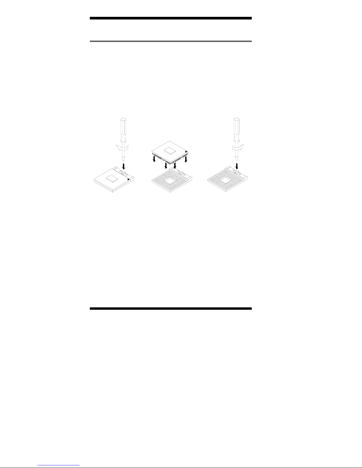
CPU Socket mPGA 478MT Socket
Chipset Intel 945GM Chipset
GMCH: 82945GM 1466-pin Micro-FCBGA
ICH7M: 82801GBM 652-pin mBGA
BIOS Award BIOS, support ACPI Function
Memory DDR2 667/533 SDRAM DIMM x2 (w/o ECC function), Max. 4GB
VGA 945GM built-in, supports CRT, RCA, S-VIDEO, HDTV
PCIEx16 SLOT For External PCI Express Based graphics card
LVDS LCD Panel 945GM built-in, supports 18+18 bits, single or dual channel LVDS
LAN 1. ICH7M built-in 10/100BT MAC + Intel 82562ET PHY
2. Marvell 88E8053 PCI Express Gigabit LAN controller x1
USB ICH7M built-in USB 2.0 host controller, support 6 ports
Serial ATA Ports ICH7M built-in SATA controller, supports 2 ports
Parallel IDE ICH7M built-in one channel Ultra DMA 33/66/100,CF
Audio ICH7M Built-in Audio controller + AC97 Codec ALC655 w/ 6 channels
(Line-out, Line-in, Mic.), SPDIF-OUT + NS LM4950 (8-ohm 2W stereo
audio power amplifier)
LPC I/O W83627EHF: COM1, COM2 (RS232), Slim FDC 1.44MB, IrDA x1 &
hardware monitor (3 thermal, 4 voltage monitor inputs, 2 fan headers)
Fintek F81216: COM3, COM4 (RS232)
Digital IO 4 in & 4 out
Keyboard/Mouse Supports PS/2 Keyboard/Mouse Connector
Expansion Slots PIC-E (x16) slot x1 and Mini PCI socket x1, Mini PCIe X1
Edge Connector PS/2 Connector x1 for keyboard/mouse
Gbit LAN RJ-45 + dual USB stack connector
10/100 LAN RJ45 + dual USB stack connector
DB9 x1 for COM 1; DB15 x1 for VGA
RCA Jack x1 +S-Video for TV-Out
SPDIF-OUT connector x1
RCA Jack 3x1 for Audio (Line-Out, Line-In & Mic)
Onboard Header/
Connector 40 pins box-header x1 for IDE1; 26 pins header x1 for Slim Floppy
CF Connector x1 @ solder side
10 pins pin-header x1 for Digital I/O;9 pins pin-header x3 for COM2~COM4
8 pins pin-header x 1 for USB 5,6; 5 pins pin-header x 1 for IrDA
DF13 Connector x2 for LVDS; 8 pins pin-header x1 for HDTV
7 pins pin-header x1 for audio Line-Out & Mic
4 pins pin-header x1 for built-in speaker
SATA connector x2 for 2 SATA ports
Watchdog Timer Yes (256 segments, 0, 1, 2…255 sec/min)
System Voltage +5V, +3.3V, +12V, -12V, 5VSB (2A)
Others Modem Wakeup, LAN Wakeup
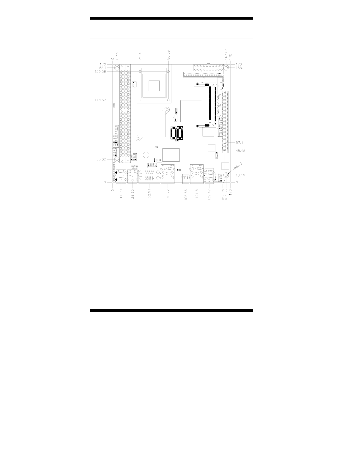
Board Size 170mm x 170mm (Mini ITX)

INTRODUCTION
4MB899X User’s Manual
[
Board Dimensions

INSTALLATIONS
MB899X User’s Manual 5
Installations
This section provides information on how to use the jumpers and
connectors on the MB899X in order to set up a workable system. The
topics covered are:
Installing the CPU........................................................................ 6
Installing the Memory.................................................................. 7
Setting the Jumpers...................................................................... 8
Connectors on MB899X............................................................ 11

INSTALLATIONS
6MB899X User’s Manual
Installing the CPU
The MB899X board supports a Socket 478MT (Napa) processor socket
for Intel® CoreTM 2 Duo , Intel® CoreTM Duo and Intel® CoreTM Solo
mobile processors.
The processor socket comes with a screw to secure the processor. As
shown in the left picture below, loosen the screw first before inserting
the processor. Place the processor into the socket by making sure the
notch on the corner of the CPU corresponds with the notch on the inside
of the socket. Once the processor has slide into the socket, fasten the
screw. Refer to the figures below.
NOTE: Ensure that the CPU heat sink and the CPU top surface are in
total contact to avoid CPU overheating problem that would
cause your system to hang or be unstable.

INSTALLATIONS
MB899X User’s Manual 7
Installing the Memory
The MB899X board supports two DDR2 memory socket for a maximum
total memory of 4GB in DDR2 memory type.
Installing and Removing Memory Modules
To install the DDR2 modules, locate the memory slot on the board and
perform the following steps:
1. Hold the DDR2 module so that the key of the DDR2 module align
with those on the memory slot.
2. Gently push the DDR2 module in an upright position until the clips of
the slot close to hold the DDR2 module in place when the DDR2
module touches the bottom of the slot.
3. To remove the DDR2 module, press the clips with both hands.
DDR2 Module
Lock Lock
Lock Lock

INSTALLATIONS
8MB899X User’s Manual
Setting the Jumpers
Jumpers are used on MB899X to select various settings and features
according to your needs and applications. Contact your supplier if you
have doubts about the best configuration for your needs. The following
lists the connectors on MB899X and their respective functions.
Jumper Locations on MB899X.......................................................9
JP2: CPU FSB Selection (reserved)..............................................10
JP5: LCD Panel Power Selection..................................................10
JP7: Clear CMOS Setting.............................................................10
JP8: CompactFlash Slave/Master Selection..................................10
JP9: Internal/External VGA Selection..........................................10

INSTALLATIONS
MB899X User’s Manual 9
Jumper Locations on MB899X
Jumpers on MB899X........................................................................Page
JP2: CPU FSB Selection .............................................................. 10
JP5: LCD Panel Power Selection................................................. 10
JP7: Clear CMOS Setting............................................................. 10
JP8: CompactFlash Slave/Master Selection ................................. 10
JP9: Internal/External VGA Selection.......................................... 10

INSTALLATIONS
10 MB899X User’s Manual
JP2: CPU FSB Selection (reserved)
JP2 CPU FSB
533MHz
667MHz
JP5: LCD Panel Power Selection
JP5 LCD Panel Power
3.3V
5V
JP7: Clear CMOS Setting
JP7 Setting
Normal
Clear CMOS
JP8: CompactFlash Slave/Master Selection
JP8 CF Setting
Master
Slave
[
JP9: Internal/External VGA Selection
JP9 VGA Source
Internal
External

INSTALLATIONS
MB899X User’s Manual 11
Connectors on MB899X
The connectors on MB899X allows you to connectexternal devices such
as keyboard, floppy disk drives, hard disk drives, printers, etc. The
following table lists the connectors on MB899X and their respective
functions.
CN1: PS/2 Keyboard and PS/2 Mouse Connectors...................... 13
CN2, CN3: COM1 and VGA Connector...................................... 13
CN4: 10/100 RJ-45 and USB1/2 Ports......................................... 14
J12: SPDIF Out Connector........................................................... 14
CN6, CN7: GbE RJ-45 and USB3/4 Ports................................... 14
CN8: Audio Connector................................................................. 14
CN9, CN10: Serial ATA Connectors........................................... 14
FAN1: System Fan Power Connector .......................................... 14
FAN2: CPU Fan Power Connector .............................................. 14
IDE1: IDE Connector................................................................... 15
FDD1: Floppy Drive Connector................................................... 15
J14: ATX Power Supply Connector............................................. 16
J1: IrDA Connector...................................................................... 16
J2: Digital I/O............................................................................... 16
J3: System Function Connector.................................................... 17
J4: TV-OUT (S-Video & Composite) Connector......................... 18
J5: TV-OUT (Y, Pr, Pb) Connector ............................................. 18
J6: USB5/6 Port Pin Header......................................................... 19
J7,J21,J22: COM2,3,4 Serial Port................................................ 19
J8: Wake On LAN Connector ...................................................... 19
J9, J10: LVDS Connectors (1st channel, 2nd channel)................ 20
J11: LCD Backlight Connector .................................................... 20
J13: Mini PCI Connector.............................................................. 20
U36: Mini PCI- E(x1) Connector................................................. 20
J15: Speaker Connector................................................................ 20
J17: Front Audio Connector......................................................... 21
PCIEX16: PCI-E(x16) Slot.......................................................... 21
J19: CD-In Pin Header................................................................. 21
J20: Compact Flash Connector..................................................... 21

INSTALLATIONS
12 MB899X User’s Manual
Connector Locations on MB899X

INSTALLATIONS
MB899X User’s Manual 13
CN1: PS/2 Keyboard and PS/2 Mouse Connectors
PS/2 Mouse
PS/2 Keyboard
Signal Name Keyboard Mouse Signal Name
Keyboard data 1 1 Mouse data
N.C. 2 2 N.C.
GND 3 3 GND
5V 4 4 5V
Keyboard clock 5 5 Mouse clock
N.C. 6 6 N.C.
CN2, CN3: COM1 and VGA Connector
[ Signal Name Pin # Pin # Signal Name
DCD 1 6 DSR
RXD 2 7 RTS
TXD 3 8 CTS
DTR 4 9 RI
GND 5 10 Not Used
[[[[ Signal Name Pin # Pin # Signal Name
Red 1 2 Green
Blue 3 4 N.C.
GND 5 6 GND
GND 7 8 GND
N.C. 9 10 GND
N.C. 11 12 N.C.
HSYNC 13 14 VSYNC
NC 15

INSTALLATIONS
14 MB899X User’s Manual
CN4: 10/100 RJ-45 and USB1/2 Ports
J12: SPDIF Out Connector
CN6, CN7: GbE RJ-45 and USB3/4 Ports
CN8: Audio Connector
The audio connector, from top to bottom, is composed of Line in, Line
out and Microphone jacks.
CN9, CN10: Serial ATA Connectors
FAN1: System Fan Power Connector
FAN1 is a 3-pin header for system fans. The fan must be a 12V
(500mA).
Pin # Signal Name
1 Ground
2 +12V
3 Rotation detection
FAN2: CPU Fan Power Connector
FAN2 is a 3-pin header for the CPU fan. The fan must be a 12V fan.
Pin # Signal Name
1 Ground
2 +12V
3 Rotation detection

INSTALLATIONS
MB899X User’s Manual 15
IDE1: IDE Connector
Signal Name Pin # Pin # Signal Name
Reset IDE 1 2 Ground
Host data 7 3 4 Host data 8
Host data 6 5 6 Host data 9
Host data 5 7 8 Host data 10
Host data 4 9 10 Host data 11
Host data 3 11 12 Host data 12
Host data 2 13 14 Host data 13
Host data 1 15 16 Host data 14
Host data 0 17 18 Host data 15
Ground 19 20 Protect pin
DRQ0 21 22 Ground
Host IOW 23 24 Ground
Host IOR 25 26 Ground
IOCHRDY 27 28 Host ALE
DACK0 29 30 Ground
IRQ14 31 32 No connect
Address 1 33 34 No connect
Address 0 35 36 Address 2
Chip select 0 37 38 Chip select 1
Activity 39 40 Ground
FDD1: Floppy Drive Connector
FDD1is a slim 26-pin connector and will support up to 2.88MB FDD.
Signal Name Pin # Pin # Signal Name
VCC 1 2 INDEX
VCC 3 4 DRV_SEL
VCC 5 6 DSK_CH
NC 7 8 NC
NC 9 10 MOTOR
DINST 11 12 DIR
NC 13 14 STEP
GND 15 16 WDATA
GND 17 18 WGATE
GND 19 20 TRACK
NC 21 22 WPROT
GND 23 24 RDATA
GND 25 26 SIDE

INSTALLATIONS
16 MB899X User’s Manual
J14: ATX Power Supply Connector
Signal Name Pin # Pin # Signal Name
3.3V 11 1 3.3V
-12V 12 2 3.3V
Ground 13 3 Ground
PS-ON 14 4 +5V
Ground 15 5 Ground
Ground 16 6 +5V
Ground 17 7 Ground
-5V 18 8 Power good
+5V 19 9 5VSB
11 1
20 10 +5V 20 10 +12V
J1: IrDA Connector Pin # Signal Name
1 +5V
2 No connect
3 Ir RX
4 Ground
5 Ir TX
J2: Digital I/O
Signal Name Pin Pin Signal Name
GND 1 2 VCC
OUT3 3 4 OUT1
OUT2 5 6 OUT0
IN3 7 8 IN1
IN2 9 10 IN0
Table of contents
Other Award Motherboard manuals