INTRODUCTION
MI812 User’s Manual 3
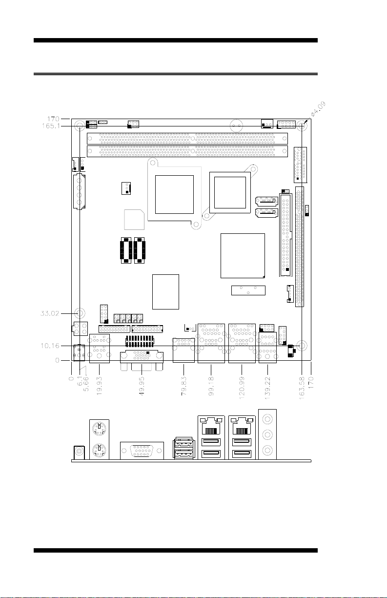
MI812 Specifications
CPU Type Intel® Atom™ N270 processor (45nm)
CPU FSB CPU Clock speed = 1.60GHz
FSB=533MHz
L2 Cache=512K
TDP=2.5W
Green /APM APM1.2
BIOS Award BIOS, support ACPI function
Chipset Intel 945GSE Chipset
GMCH: 82945GSE 27mm x 27mm -998-pin FCBGA
ICH7M: 82801GBM 31mm x 31mm -652-pin BGA
Memory DDRII 533 DIMM x2. Max. 2GB
Supports Single channel, without ECC function
VGA 945GSE built-in, Intel® Graphics Media Accelerator 950 Graphics
Core, Supports CRT
LVDS Chrontel 7308B for 18/24-bit dual channel LVDS interface
LAN 1. ICH7M built-in 10/100BaseT MAC + Intel 82562ET PHY
2. Intel 82574L PCI-Express Gigabit LAN controller x1
USB ICH7M built-in USB 2.0 host controller, support 8 ports
Serial ATA Ports ICH7M built-in SATA controller, supports 2 ports
Parallel IDE ICH7M built-in one channel Ultra DMA 33/66/100, CF
Audio ICH7M built -in audio controller w/ ALC 662 HD audio codec
5.1-channel (Line-in, Line-out & Microphone)
LPC I/O Winbond W83627EHG: COM1 (RS232), COM2 (RS232/422/485),
LPT port; Hardware monitor (3 thermal inputs, 4 voltage monitor
inputs, VID0-4 & 2 fan headers)
2’nd LPC I/O Fintek F81216DG COM3 & COM4(RS232)
Digital IO 4 in & 4 out
Keyboard/Mouse Supports PS/2 Keyboard/Mouse connectors
Expansion Slots PCI slot x1, PCI-E (x1) slot x1 and Mini PCI-E (x1) socket x1
Power Connector DC power jack x1 for +12V/+19V DC-in
Edge Connectors PS/2 connector x1 for keyboard/mouse
Gigabit LAN RJ-45 + dual USB stack connector
10/100 LAN RJ45 + dual USB stack connector
Dual USB stack connector for USB5/USB6
DB15 connector for VGA output
3x1 stack mini jacks (0.125”) for HD audio (Line-in, Line-Out,
Microphone); DC-in jack
Onboard
Header/Connectors DF13 connector x2 for LVDS
SATA connector x2 for 2 SATA ports
40-pin box-header x1 for IDE1
CF Connector x1 @ solder side
8-pin header x1 for USB 7,8
20-pin header x1 for LPT port
20-pin DF11 connector x2 for COM1/COM2, COM3/COM4
(Powered with 5V or 12V or as ring-in)
10-pin header x1 for audio Line-Out & Microphone
10 pin-headerx1 for Digital I/O
Watchdog Timer Yes (256 segments, 0, 1, 2…255 sec/min)
Other Modem Wakeup, LAN Wakeup
RoHS Yes
Board Size 170mm x 170mm (Mini ITX form factor)