PCI8735DataAcquisition V6.018
Contents
Contents............................................................................................................................................................................. 1
Chapter 1 Overview........................................................................................................................................................... 2
Chapter 2 Components Layout Diagram and a Brief Description .................................................................................... 4
2.1 The Main Component Layout Diagram ............................................................................................................... 4
2.2 The Function Description for the Main Component ............................................................................................ 4
2.2.1 Signal Input and Output Connectors ......................................................................................................... 4
2.2.2 Potentiometer ............................................................................................................................................ 4
2.2.3 Physical ID of DIP Switch ........................................................................................................................ 4
Chapter 3 Signal Connectors............................................................................................................................................. 6
3.1 The Definition of Signal Input Connectors .......................................................................................................... 6
3.2 DI Definition of Signal Input and Output Connectors ......................................................................................... 6
3.3 DO Definition of Signal Input and Output Connectors........................................................................................ 7
Chapter 4 Connection Ways for Each Signal..................................................................................................................... 8
4.1 AD Single-ended Input Connection ..................................................................................................................... 8
4.2 AD Double-ended Input Mode............................................................................................................................. 8
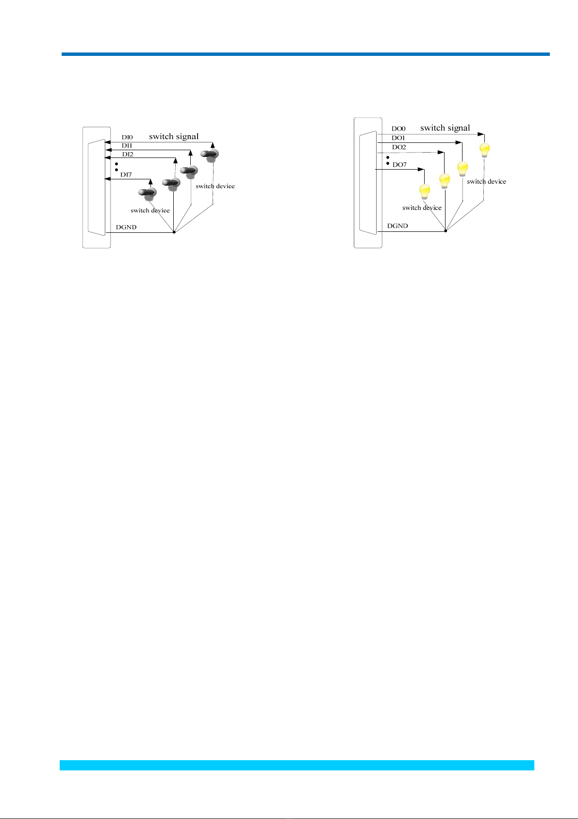
4.3 DIO Connection ................................................................................................................................................... 9
Chapter 5 Notes, Calibration and Warranty Policy......................................................................................................... 10
5.1 Notes .................................................................................................................................................................. 10
5.2 AD Analog Signal Input Calibration.................................................................................................................. 10
5.3 Warranty Policy.................................................................................................................................................. 10
Products Rapid Installation and Self-check ..................................................................................................................... 12
Rapid Installation ..................................................................................................................................................... 12
Self-check ................................................................................................................................................................ 12
Delete Wrong Installation ........................................................................................................................................ 12
BUY ONLINE at www.art-control.com/englishs or CALL (86)-10-62991792-609 1